Wednesday, November 13, 2019
 

Disruptive Computing

Chair Patrick Bressler, Managing Director, Fraunhofer Group for Microelectronics
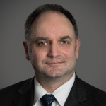
Patrick Bressler

Patrick Bressler
Managing Director
Fraunhofer Group for Microelectronics

Patrick Bressler

Biography
Patrick Bressler is currently the managing director for the Fraunhofer Group for Microelectronics. The group consists of 17 Fraunhofer Institutes with a total research budget of €439M and +3000 staff (2017), dedicated to technology development and technology-based innovation in micro- and nanoelectronics. Before that Dr. Bressler was the Executive Vice President of Fraunhofer USA, the US subsidiary with an annual budget of +$42M and +160 staff, and adjunct professor at the department of computer science and engineering at Michigan State University. Patrick has held various executive positions in Europe and the US, in basic research, technology validation and technology-based business and entrepreneurship, such as technology expert and Fraunhofer representative to the European Commission in Brussels. By training a physicist, Patrick holds a PhD in surface and semiconductor physics from the Technical University Berlin.

12:45
Diamond for Quantum Computing
  Rüdiger Quay, Deputy Director, Fraunhofer Institute
Diamond for Quantum Computing

Rüdiger Quay

Rüdiger Quay
Deputy Director
Fraunhofer Institute

Rüdiger Quay

Abstract
Quantum computers exploit the phenomenon of quantum superposition, or the counterintuitive ability of small particles to inhabit contradictory physical states at the same time. An electron, for instance, can be said to be in more than one location simultaneously, or to have both of two opposed magnetic orientations. Where a bit in a conventional computer can represent zero or one, a qubit can represent zero, one, or both at the same time. It’s the ability of strings of qubits to simultaneously explore multiple solutions to a problem that promises computational speedups.Diamond-defect qubits result from the combination of “vacancies,” which are locations in the diamond’s crystal lattice where there should be a carbon atom but there isn’t one, and “dopants,” like nitrogen atoms placed in direct neighborhood to the vacancy. Together, the dopant and the vacancy create a donor-vacancy center, which has a free electron associated with it. The electrons magnetic orientation, or spin, which can be in superposition, constitutes the qubit. Donor-vacancy centers in diamond potentially can work at room temperature and are therefore considered a very attractive technology for building quantum networks. The biggest drawback to donor-vacancy centers in diamond is the difficulty of fabrication. Researchers either look for naturally-occurring defects in diamond, or fire atoms at a piece of diamond at high energy, creating defects in modulation doped lattice. We review the remarkable progress made in the past years in controlling electrons, atomic nuclei, and light at the single-quantum level in diamond. We also discuss prospects and challenges for the use of donor-vacancy centers in future quantum technologies.

Biography
Rüdiger Quay received the Diplom-degree in physics from Rheinisch-Westfälische Technische Hochschule (RWTH), Aachen, Germany, in 1997, and a second Diplom in economics in 2003. In 2001 he received his doctoral degree in technical sciences (with honours) from the Technische Universität Wien, Vienna, Austria. In 2009 he received the venia legendi (habilitation) in microelectronics, again from the Technische Universität Wien. In 2001 he joined the Fraunhofer Institute of Applied Solid-State Physics Freiburg in various positions. He is currently the deputy director of Fraunhofer IAF and responsible for the business fields. Since 2011 he is also a lecturer at the IMTEK, Albert-Ludwig University, Freiburg, Germany. Dr. Quay has authored and coauthored over 250 refereed publications, three monographs and contributions to two further. He holds two patents.

13:05
Disruptions Ahead – Hearings Instruments as Multi-Sensor Platforms
  Uwe Andreas Hermann, Senior Director, Eriksholm Research Center
Disruptions Ahead – Hearings Instruments as Multi-Sensor Platforms
Uwe Andreas Hermann

Uwe Andreas Hermann
Senior Director
Eriksholm Research Center

Uwe Andreas Hermann

Abstract
Imagine a Hearing Instrument (HI) which disappears in your ear, is comfortable to be worn 7 * 24, packed with bio-sensors, Artificial Intelligence and Connectivity. What could it mean for you and what could it mean for our society and healthcare systems? - The possibilities of such HIs are almost unlimited. They range from consumer functions already known today like handsfree telephony, music streaming, voice over internet, “personal butler” (like Alexa or Siri to go), instant translation all the way to the most advanced medical services.Eriksholm has - together with a European research consortium – just finished a very successful Horizon 2020 project, where some of the almost infinite applications of EEG sensors integrated into a hearing Instrument have been proven. Imagine a HI which reads your mind and intuitively does what you want!And this is only the very beginning of an exciting journey fueled by more and more powerful silicon engines. In our labs you can see experimental versions with build in infrared sensors, so called ppg, as well as motion-, temperature or skin-resistance-sensors. Artificial intelligence will bind all these sensors together and create a so called “sensor fusion” which allows completely new Hearing Healthcare solutions, but also an almost infinite amount of general healthcare solutions.Global healthcare services are looking into exploding costs, driven by an aging population and increased patient expectations. The solution to this global challenge is prevention. It is all about early detection of diseases allowing for (cost) effect early treatment. Imagine how much healthcare systems will save, when we are able e.g. to avoid just a few percentage points of dementia cases due to early detection and treatment! - The Hearing Instruments of the future will be a central element of the solution.For the hearing instrument industry the best is yet to come!

Biography
Uwe A. Hermann, MSc, Senior DirectorUwe A. Hermann is since September 2013 Head of the Eriksholm Research Centre, about 50 km north of Copenhagen. This research center belongs to Oticon, one of the biggest providers of hearing instruments and hearing healthcare solutions worldwide. Main areas of research are “Augmented Hearing Science” for audiological applications, “Cognitive Hearing Science” for brain hearing applications and “Social Hearing Science”. Before Uwe worked for 17 years for Siemens in Munich in various management positions. Here his main focus was Innovation and Technology management. Amongst other assignments, he was a Principal Consultant for the Siemens Board of Directors (“Zentralvorstand”) with responsibility for the global Siemens network of university collaborations. In parallel Uwe has been a lecturer at the University of Duisburg-Essen for more than 10 years.

13:25
Enablement of Energy-efficient Machine Learning hardware through System-Technology Co-optimization
  Arindam Mallik, Program Manager, imec
Enablement of Energy-efficient Machine Learning hardware through System-Technology Co-optimization
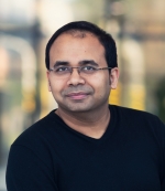
Arindam Mallik

Arindam Mallik
Program Manager
imec

Arindam Mallik

Abstract
The demand for deep learning and statistical inference is driving the hardware industry towards Machine Learning (ML)-specialized hardware. Conventional solutions for efficient computation of ML-based tasks are based on GPU architectures possibly with specialization for ML, heterogeneous system level integration with CPU and FPGA, and full ASIC implementations. We propose system-technology co-optimization: the co-optimization of algorithm, architecture, circuit and novel devices in a single framework to develop optimized technology for Machine Learning.Energy-efficiency of ML hardware implementations is a key target. In many embedded applications it is not possible, due to energy and latency constraints, to use cloud-based ML implementations. Data analysis at the source of the data, provides the opportunity to embed intelligence in the devices, avoiding the need to send raw data to the cloud for analysis, and in this way obtain vastly more energy efficient and low latency solutions for truly smart devices.In this presentation, we will discuss the following topics:Novel technology solutions (memory and logic devices) that are optimized for executing ML inference algorithm in the hardware.Co-optimization of ML algorithm and system architecture to reduce the memory bottleneck and power consumption, allow for a minimization of required memory space and minimize the occupied silicon area (i.e. chip cost) while maintaining target accuracy, latency and throughput.Development of prototype silicon to showcase the capability of the proposed approaches on industry-standard benchmarks for Machine Learning.

Biography
Arindam Mallik is Machine Learning Program Manager at imec.He received his M.S, and PhD degree in Electrical Engineering and Computer Science from Northwestern University, USA in 2004 and 2008, respectively. Arindam is a technologist working on Design Technology Co-Optimization techniques for the past 15 years. He currently manages imec’s Machine Learning Program, focusing on technology innovation needed for optimum performance of Machine Learning/Artificial Intelligence platforms. His research interests include system/design-technology co-optimization, economics of semiconductor manufacturing, and system-level analysis of advanced technology nodes. He has authored or co-authored more than 100 papers in international journals, conference proceedings, and holds number of international patent families.

13:45
Silicon for large scale quantum computing
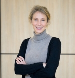

  Maud Vinet, CEA
Silicon for large scale quantum computing
Maud Vinet

Maud Vinet

CEA

Maud Vinet

Abstract
We have put a multidisciplinary and multi institutions team which gathers quantum physicists, integration and devices engineers, circuit designers and quantum information engineers. We want to build a quantum processor. We are aiming at delivering prototypes with a 100 qubits within 6 years and at having identified the key scientific and roadblocks for scaling up.Quantum computing is expected to extend the high performance computing roadmap at the condition to be able to run a large number of errorless quantum operations, typically over a billion. It is out of reach in actual physical systems because of the quantum decoherence. Therefore, quantum error correction techniques, which utilize the idea of redundant encoding combined with entanglement, have been introduced to cure for the errors. They come with an overhead in terms of qubits which induce a potential need for millions of qubits.Because of these large numbers of operations and physical qubits, Si-based QC appears as a promising approach to build a quantum processor; thanks to the size of the qubits, the quality of the quantum gates and the VLSI ability to fabricate billions of closely identical objects. The quality of Si spin qubits has improved very fast with the introduction of isotopically purified 28Si, as observed by multiple research groups. In this presentation, we will discuss the architectures to design a large scale quantum computer based on Si spin qubits and we will review their pros and cons regarding variability assumptions and technological achievements.

Biography
Maud Vinet is Leti quantum hardware director.She defended her PhD in physics from University of Grenoble Alps in 2001. She joined CEA-Leti as a CMOS integration and device engineer in 2001. From 2009-2013, she was a Leti assignee with IBM Alliance in Albany to develop FDSOI with STMicroelectronics and GlobalFoundries. In 2013, she was appointed Advanced CMOS manager in Leti. Her team investigate CMOS based solutions to shape advanced devices and computing roadmaps. As such she has been leading Si based quantum computing project since 2015. Her Google h-index = 40, >5800 citations, >140 papers and > 70 patents related to nanotechnology.

14:05
Ambipolar quantum dots in planar silicon
  Floris Zwanenburg, Associate Professor, University of Twente
Ambipolar quantum dots in planar silicon
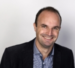
Floris Zwanenburg

Floris Zwanenburg
Associate Professor
University of Twente

Floris Zwanenburg

Abstract
We create ambipolar quantum dots in planar silicon nanoscale transistors. We first investigate the conformity of Al, Ti and Pd nanoscale gates by means of transmission electron microscopy [1]. Next we define low-disorder electron quantum dots with Pd gates [2], and depletion-mode hole quantum dots in undoped silicon [3]. For the latter we use fixed charge in a SiO2/Al2O3 dielectric stack to induce a 2DHG at the Si/SiO2 interface. The depletion-mode design avoids complex multilayer architectures requiring precision alignment and allows directly adopting best practices already developed for depletion dots in other material systems. Finally, I will show ambipolar charge sensing: we have fabricated a single-electron transistor next to a single-hole transistor, and tuned both quantum dots to simultaneously sense charge transitions of the other quantum dot. Using active charge sensing the single-hole transistor can detect the few-charge regime in the electron quantum dot.[1] P. C. Spruijtenburg et al., Nanotechnology, (2018).[2] M. Brauns et al., Scientific Reports 8, 5690, (2018).[3] S. V. Amitonov et al., Applied Physics Letters 112, 023102 (2018).

Biography
Floris Zwanenburg (1976) studied applied physics at the TU Delft. In 2008 he received his PhD for research on semiconductor nanowires with Leo Kouwenhoven. As a post-doc at UNSW in Sydney he worked with silicon quantum dots. This system has a unique fabrication scheme offering unprecedented control over all relevant parameters, as he demonstrated by reaching the single-electron regime in a highly tunable Si quantum dot. With his team at UNSW he has also used this system to read out the spin of a single electron (Nature, 2010) and to create a nuclear spin qubit (Nature, 2013). In 2011, he returned to the Netherlands for a tenure track position at the University of Twente. After initial collaborative efforts with the Dzurak team from UNSW on silicon quantum-dot technology, his team has extended this design to an ambipolar circuit, with which he has defined electron and hole quantum dots in a single device. Since 2013 he has had a new project on quantum dots and superconductivity in Ge/Si core/shell nanowires. In the past ten years he has become an expert in silicon quantum electronics: the quantum mechanical behaviour of single electron or hole spins confined to (artificial) atoms in silicon.

14:25
Advances in Energy Efficient Neuromorphic Computing: Ready for Artificial Intelligence at the Edge?
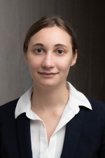
  Elisabetta Corti, researcher in the Science & Technology, Ibm
Advances in Energy Efficient Neuromorphic Computing: Ready for Artificial Intelligence at the Edge?
Elisabetta Corti

Elisabetta Corti
researcher in the Science & Technology
Ibm

Elisabetta Corti

Abstract
In this presentation we will present most recent technological advances in neuromorphic computing and their readiness to serve energy efficient artificial intelligence applications from Cloud to the Edge, with emphasis on Edge AI applications and challenges. We will particularly present progress in memristive and phase-change technologies for neuromorphic devices and system archhitectures, in comparison with CMOS implementations. We will address questions such as : (1) will spike-based neuromorphic systems be more successful than the artificial neural networks and (2) can they really be much faster and more efficient than biology? We will outline trends and challenges in the path towards successful implementations of learning systems that could be ubiquitously deployed for a large variety of cognitive computing and sensing at the Edge.

Biography
Elisabetta Corti is a researcher in the Science & Technology department at IBM Research, Zurich. In parallel, she is working towards a Ph.D. degree in Electrical Engineering under the supervision of Prof. Adrian Mihai Ionescu at EPFL, Lausanne. Her research focuses on advanced and exploratory architectures for neuromorphic computing applications. In 2018 she presented her work at the International Conference of Rebooting Computing, held in the framework of The International Roadmap for Devices and System, a research and industrial summit to project the future 15-20 years of electronic technologies. Prior to her engagement with IBM and EPFL, Elisabetta interned at imec, Belgium, researching structures for spinwave-based devices for logic applications. She holds a Master degree in Electronics Engineering from Politecnico di Milano, Italy.

14:45 End