Wednesday, November 13, 2019
 

Exhibitors Presentation

10:00
Simplifying your tool automation
  Doug Suerich, Product Evangelist, PEER Group
Simplifying your tool automation
Doug Suerich

Doug Suerich
Product Evangelist
PEER Group

Doug Suerich

Abstract
Fabs are under continuous pressure to increase throughput, maximize yield, and reduce costs. These demands produce demanding equipment purchase specifications and place strict requirements on OEMs to provide more advanced automation and data management capabilities. Additionally, these requirements create an increasing burden on OEMs to provide best-in-class automation software to complement their process expertise. The best OEMs are making strategic decisions to ensure they can meet these factory needs efficiently today and in the future.Join us as we discuss how you can streamline the delivery of your tool automation, allowing your engineers to focus on your core capabilities, while ensuring rapid deployment of SEMI standards-compliant equipment automation software, enabling fast fab acceptance of your tools.

Biography
Doug Suerich is Product Evangelist at The PEER Group Inc., the semiconductor industry’s leading supplier of factory automation software for smart manufacturing and Industry 4.0. Doug focuses on big data and remote connectivity solutions that help manufacturers collaborate securely on tools and data in production environments. A passionate advocate for smart manufacturing, Doug serves as an active member of the SEMI® Smart Manufacturing Advisory Council and SEMI SMART Manufacturing Technology Community, Americas Chapter.Doug has over 20 years of experience leading software teams for a variety of industries including semiconductor, manufacturing, and transportation. Most recently, he was involved in architecting PEER Group’s remote connectivity solution, Remicus™, and he was a champion in promoting the use of cloud computing and latest-generation web technologies.Prior to joining PEER Group, Doug was a software development manager, automation engineer, information systems specialist, and consultant. He has extensive experience designing and integrating robust automation software solutions. Doug holds a Bachelor of Applied Science with Honours in System Design Engineering from the University of Waterloo.

10:15
Towards Research 4.0 - Automating R&D with Flextura PVD and Integrated Advanced Analytics
  Christian Kjelde, International Sales, Polyteknik AS
Towards Research 4.0 - Automating R&D with Flextura PVD and Integrated Advanced Analytics
Christian Kjelde

Christian Kjelde
International Sales
Polyteknik AS

Christian Kjelde

Abstract
Polyteknik AS designs and manufactures sputtering and evaporation systems for industry and R&D. Here presenting a recent delivery of a state-of-art Flextura PVD cluster tool with in-system analysis for ambitious research within semiconducting oxides.We aim at increasing R&D throughput, reliability, quality and record massive amounts of data for further interpretation. This is done by automating and coupling smart material-/process development with in-system characterisation. With other words we are looking into RESEARCH 4.0!

Biography
Christian holds a M.Sc Eng. in Nanomaterials from Aalborg University and is responsible for sales of PVD systems at Polyteknk AS.This includes a strong impact to the development of processes and solutions for customers working in a diversified area of business fields covering semicon, mems, optoelectronics, sensors, RF, EMI etc. Furtmore the customer pallette of Polyteknik AS is ranging from volume production to almost fundamental research. A strong team colleages has succeded in transfering customer input to a robust platform which is able to bridge R&D and production in a seldom seen manner.

11:45
Sub-Angström controlled Sputtering Process for Magnetic Sensor
  Berthold Ocker, Head of Business Unit Semiconductor NDT, Singulus Technologies AG
Sub-Angström controlled Sputtering Process for Magnetic Sensor
Berthold Ocker

Berthold Ocker
Head of Business Unit Semiconductor NDT
Singulus Technologies AG

Berthold Ocker

Abstract
Over a long period the Hall sensor dominated the magnetic field measurement. In the last years more advanced magnetic sensors are under development for consumer, industrial and automobile applications. The magnetic sensors, which are using the Tunnel Magnetic Junctions, are showing the highest resitance change with a TMR of ~ 250%. For this technology it is essential to controll the film layer thickness in a sub Anström level. Singulus developed a production technology which shows a high repeatability and an excellent uniformity for a substrate size of 200 or 300 mm.

Biography
Berthold Ocker studied physics at the Johann-Wolgang-Goethe University in Frankfurt and has more than 25 year experience in the vaccum deposition technology. He started his carreer 1991 at Leybold and leaded since 2001 the R&D activitivies for spintronic apllications. Since 2015 he took over the responsiblity of the Business Unit Semiconductor NDT. He is author and co-author of more than 50 scientific articles.

12:15
Carrier Wafers for thin wafer handling using temporary bonding technologies
  Carsten Wesselkamp, Sales Manager, Plan Optik AG
Carrier Wafers for thin wafer handling using temporary bonding technologies
Carsten Wesselkamp

Carsten Wesselkamp
Sales Manager
Plan Optik AG

Carsten Wesselkamp

Abstract
Microelectromechanical systems (MEMS) and Sensors provide the magic that makes today’s devices from our everyday life smart. MEMS consist of tiny mechanical and electrical devices such as membranes, mirrors and valves, as well as sensors, actuators and integrated circuits. Without MEMS or sensors, we would not have smartphones, smart homes and wearable smart watches, as well as a huge range of industrial and medical devices that require the functionality provided by MEMS and sensors.Smaller package sizes require extremely thin substrates to build up devices. For this thin and ultra-thin substrates need to be processed, that put new challenges on handling them throughout the process. For this carrier wafers are used, that support the thin device wafer during processing.Temporary bonding and de-bonding is used to fix the device wafer onto the carrier prior to processing and releasing it afterwards. There are different bonding and de-bonding technologies available, that require different material properties as well as patterns and features.Glass and quartz are excellent materials for carrier wafers because of their thermal stability and resistance against acids and other chemicals. Bonding to and de-bonding from glass and quartz carrier wafers can be monitored since they are transparent. Furthermore, glass carrier wafers can be cleaned and re-used, thus contributing to cost reduction and environmental protection.This presentation shows possibilities for using Carriers from Glass and Quartz with different bonding and de-bonding technologies as laser, chemical or thermal release.

Biography
Mr. Carsten Wesselkamp got a degree in Industrial Engineering with a study emphasis on operating technology and production engineering in 1995. He additionally achieved a certifcate in work system and process organization by REFA (organization for work study and company organization).After working as assistant production manager for a multinational steel and aluminum producer he joined Plan Optik AG, one of the leading manufacturers of wafers for MEMS and carriers for semiconductor applications in 1996 as one of their sales engineers.Since many years, Mr. Wesselkamp acts as the international sales manager of Plan Optik AG and (together with his team) manages the accounts of Plan Optik AG including all technical and commercial tasks.

12:30
Two-photon absorption in semiconductors design and manufacturing
  Paulius Naujalis, Sales Manager, Fyla laser
Two-photon absorption in semiconductors design and manufacturing
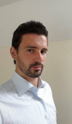
Paulius Naujalis

Paulius Naujalis
Sales Manager
Fyla laser

Paulius Naujalis

Abstract
Two-Photon absorption technique for semiconductors and circuits inspection allows precise voxel analysis in semiconductors, wafers or circuits. High flexibility new fiber laser design allows to reduce costs from existing techniques and increases flexibility in measurement capabilities.

Biography
Experienced Sales Manager/Applications Specialist with a demonstrated history of working in the photonics industry. Skilled in Relationship management, commercial department management, design and development of photonics solutions and Research and Development (R&D). Strong engineering and commercial professional with a Master in Physics, Diploma in Engineering and Certificates in Business Management.

13:30
3D Automatic X-Ray Inspection System
  Yoo Yeob Jung, CEO, Nanotech Digital GmbH (SEC Europe Head Office)
3D Automatic X-Ray Inspection System
Yoo Yeob Jung

Yoo Yeob Jung
CEO
Nanotech Digital GmbH (SEC Europe Head Office)

Yoo Yeob Jung

Abstract
TOPIC: 3D X-ray Inspection for defects in Multi Layers for the Mass production application of IC, PCB, PCBA, BGA, etc.Motivation:What is 3D AXI? It uses X-rays as its source to automatically inspect features, which are typically hidden from optical view. 3D AXI is automatically inspects the defects of products in customer's line with high-speed 3D CT tomography.Able to inspect every defect of double-sided PCBA & BGA mounted components precisely by solving overlapped X-ray image issue. Inspection speed of 4.5 sec/FOV from loading to automatic Good/NG judgement.Description:• X-Ray Tube; 160kV/500uA• Min. Resolution; 0.8~15 um• Table Size; Max.330x250mm, Min 50x50mm• Detector; 12inch FPXD• Inspection Object; BGA, Though Hole, Chip, QFN, QFP, PoP, connector, Components• Equipment Dimension; 1,360(W) x 1,880(D) x 1,700(H)/ 4,200KgInnovation:• World Fastest speed 3D In-Line Inspection• Hybrid Open Tube; - realize Best resolution of 0.8um Focal spot - realize Pulse beam and it remove CT afterimage - reduce radiation damage - realize long life span for in-line purpose• Best Solution for both-side layered PCB(HIP:Head in Pilaw)Results:Cover AVI Inspection limit -> Multi-Layer InspectionShorten 3D Inspection Time; 4.0 sec/FOV -> High Speed Inspection for Mass production Reduction of radiation damage; Max. 1/100 -> Damage Free Tube life span; 10,000hrs/Filament -> Long Life Maintenance

Biography
The founder/CEO of the company has a Master’s Degree in semiconductor and displayengineering as well as an AICPA MBA degree.He has worked as an semiconductor & display mass production equipment engineer. He hasextensive knowledge in the thin film process, and equipment process.With his expertise in various display and semiconductor equipment process, he established“Nanotech Digital GmbH,” to develop various Roll to roll CVD graphene and applied graphenetechnology products, semiconductor equipment & components. Also he has worked as an general manager of 'SEC Co.,Ltd''SEC Co.,Ltd' is the best inspection system company developing industrial X-ray inspection , SEM(Scanning Electron Microscope) and linear accelerator technology. SEC is specialized in 2D & 3D automatic X-ray inspection for semiconductor packaging, PCB, electronic components.