Tuesday, November 12, 2019
 

Challenges for Moore’s Law

Chair Markus Pfeffer, Group Manager, Fraunhofer IISB
Markus Pfeffer

Markus Pfeffer
Group Manager
Fraunhofer IISB

Markus Pfeffer

Biography
Dr. Markus Pfeffer (Fraunhofer IISB) holds a diploma in Electrical Engineering and a PhD (Dr.-Ing.) with specialization in manufacturing optimization both from the University of Erlangen- Nuremberg. Since 2002 he is with Fraunhofer IISB in the department Semiconductor Manufacturing Equipment and Methods. He is leading the group Manufacturing Control with a strong focus on equipment control, contamination control, manufacturing optimisation, equipment assessment and discrete event simulation. He was/is involved in several national and international cooperative R&D projects, e. g. FLYING WAFER, IMPROVE, EEMI450, EPPL, Productive4.0, idev40, NEREID, FED4SAE and SEA4KET in a variety of functions.

13:00
Challenges for the end of Moore Law
  Francis Balestra, Director of Research CNRS, CNRS-Grenoble INP
Challenges for the end of Moore Law
Francis Balestra

Francis Balestra
Director of Research CNRS
CNRS-Grenoble INP

Francis Balestra

Abstract
The historical trend in micro/nano-electronics over the last 50 years has been to increase both speed and density by scaling down the size of electronic devices, together with reduced energy dissipation per binary transition, and to develop many novel functionalities for future electronic systems. We are facing today dramatic challenges for More Moore and More than Moore applications: substantial increase of energy consumption and heating which can jeopardize future IC integration and performance, reduced performance due to limitation in traditional high conductivity metal/low k dielectric interconnects, limit of optical lithography, heterogeneous integration of new functionalities for future nanosystems, etc. Therefore many breakthroughs, disruptive technologies, novel materials, and innovative devices are needed in the next two decades.With respect to the substantial reduction of the static and dynamic power of future high performance/ultra low power terascale integration and autonomous nanosystems, new materials, ultimate processing technologies and novel CMOS or Beyond-CMOS device architectures (FDSOI, FinFET, Nanowire FET, Nanosheet devices, Carbon Nanotube FET, Tunnel FET or Ferroelectric Gate FET with Negative Capacitance, Non-charge-based Memories –e.g. PCRAM, ReRAM, MRAM, FeRAM- 3D integration, etc.) are mandatory for different applications, as well as new circuit design techniques, architectures and embedded software.This presentation will focus on the main trends, challenges, limits and possible solutions for future high performance and ultralow power nanoscale devices for the end of Moore’s Law.

Biography
BALESTRA Francis, CNRS Research Director at IMEP-LAHC, has been Director of several Laboratories, IMEP and LPCS, for a total of 10 years and Director of the European Sinano Institute during 6 years. Within FP6, FP7 and H2020, he coordinated several European Projects (SINANO, NANOSIL, NANOFUNCTION, NEREID) that have represented unprecedented collaborations in Europe in the field of Nanoelectronics. He is member of the AENEAS Scientific Council, of the European Academy of Sciences, of the Advisory Committee of several International Journals and of European Working Groups for Roadmapping activities. He founded (ULIS, WOLTE, INC) or organized many international Conferences, and has co-authored a large number of books and publications. He is currently Vice President of Grenoble INP, in charge of European activities.

13:25
EU consortia joining forces to tackle challenges of advanced technology nodes
  Werner Boullart, Principal Member of Technical Staff, Imec
EU consortia joining forces to tackle challenges of advanced technology nodes

Werner Boullart

Werner Boullart
Principal Member of Technical Staff
Imec

Werner Boullart

Abstract
Moore’s Law has powered more than 50 years of advances in the microelectronics industry. In recent years this law is under pressure, because the continued geometrical miniaturization led to device performance degradation, device variability issues. Since 2015, with financial support from the EU, material compagnies, equipment companies, design houses, universities and research institutes have joined forces to tackle the challenges related to CMOS scaling. The first project, SeNaTe, targeted the 7nm node, subsequent projects respectively tackled the 5nm node (TAKE5 and TAKEMI5) and the 3nm node (TAPES3 and Pin3S) challenges. Recently, May 2019, the IT2 project targeting IC Technology for 2nm node was submitted for funding by EU. An overview will be presented of the technical solutions which have been explored to provide solutions for 7nm, 5nm, 3nm technology node to keep pace with Moore’s scaling law.The following topics will be addressed: multi-patternng solutions for area scaling, self-aligned patterning and area selective deposition solutions for Edge Placement Error (EPE) mitigation, material innovation, hybrid damascene and air gap integration for advanced BEOL, innovative device architectures transitioning from planar to FinFET, Gate All Around nanowire/nanosheet (GAA NW/NS) device, for improved device performance. Other topic which will be addressed are track height scaling and device booster integration through Design Technology Co-Optimization. Device boosters which will be covered comprise: fully-Self Aligned Contact, Self-Aligned Gate Contact, Self-Aligned Block, Buried Power Rail (BPR), Super Via (SV). Final part of the presentation will cover System Technology Co-Optimization (STCO). STCO, the next level of design and technology optimization, this time approached from a system/application perspective, for manufacturing of future node devices and applications meeting 2nn node PPAC specifications.

Biography
Werner Boullart received a PhD in Chemistry in 1991 at the Catholic University of Leuven. Till 1995 he worked at the university as a researcher in the domain of atmospheric chemistry.In 1995, he joined imec as a process engineer responsible for the development of plasma etch processes. From 2001 till 2012, he was manager of the Plasma Etch group. Since 2012 he worked as staff engineer of the Unit Process and Module department responsible for strengthening the collaboration between the different unit process step groups. In this function he was also managing Joint Development Projects with key semiconductor equipment suppliers.Since 2015, he took up the role of work package project manager for imec in the EU funded projects. In this role he is also responsible for defining the the imec contribution for future projects related to advanced CMOS scaling.

13:50
Specialty Markets & More-than-Moore (MtM) Technologies
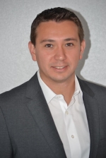
  Llew Vaughan-Edmunds, Applied Material
Specialty Markets & More-than-Moore (MtM) Technologies
Llew Vaughan-Edmunds

Llew Vaughan-Edmunds

Applied Material

Llew Vaughan-Edmunds

Abstract
Whether defined by the term More-than-Moore (MtM) or Specialty Technologies, there’s no denying the impact this segment of the semiconductor industry has had on the world over the past 25 years. MEMS, Power Devices, RF Devices, CMOS Image Sensors, Analog Devices, Photonics and Wafer Level Packaging technologies are at the heart of many of the end use device technologies we take for granted today. And, while they continue to evolve, its not often clear the central role equipment suppliers play in enabling their capabilities. This presentation will briefly discuss the MtM market that has now become synonymous with these device technologies, introduce some of the key technologies Applied Materials has contributed and outline how a company the size of Applied Materials is best positioned to work with customers and R&D organizations toward their mutual success in a rapidly changing MtM world.

Biography
Llew Vaughan-Edmunds is Director of Strategic Marketing at Applied Materials, focusing on the Power Device technologies segment.He has more than 20 years of power management experience at Infineon, International Rectifier, Fairchild and ON Semiconductor.He holds an MBA from Chapman University, BS in Applied Electronics from University of Liverpool, and a patent in GaN device technology

14:15
Interconnects, scaling and integrational aspects in 300mm R&D
  Lukas Gerlich, Project manage, Fraunhofe ipms
Interconnects, scaling and integrational aspects in 300mm R&D

Lukas Gerlich

Lukas Gerlich
Project manage
Fraunhofe ipms

Lukas Gerlich

Abstract
New challenges in diversification of materials and in integration of new concepts in the Back-End-of-Line (BEOL) emerge with further development of novel computer chips. Besides scaling of feature sizes and usage of other substitute materials for Copper as interconnect or for barriers and liners like Cobalt new memory or capacitor stacks integrated in the metallization area give a lot of opportunities as a test platform for next generation computing and beyond CMOS approaches. But also some obstacles have to be resolved like material compatibility and contamination control. This is especially important for ferroelectric Hafnium Oxide based material and new materials for MRAM and general spintronic developments. Here we will present the memory integration concept in our BEOL with new Clover chambers in an AMAT Endura system with mixed protocol zone environment for flexible R&D on 300mm. Therefore within national-, EU-funded projects and direct contract research Fraunhofer IPMS works together with the industry for finding solutions to keep technology development for more-Moore and more-than-Moore applications on track.We will also address the additional requirements for consumable and tool manufacturers, which are connected with the progress of Moore’s law. Within the FMD (Forschungsfabrik Mikroelektronik Deutschland) new tool setups and with the help of our Screening Fab approach, we enable partners to optimize their products for future scaling and integration.

Biography
Dr. Lukas Gerlich (Fraunhofer IPMS) received his PhD (Dr.-Ing.) at Brandenburg Technical University Cottbus in 2012 in the field of barrier films for Cu-metallization on 300 mm wafers and in-situ XPS characterization during his work at Fraunhofer CNT together with AMD and Globalfoundries as project partners. Since the integration of Fraunhofer CNT into IPMS in 2013, he works as project manager and was responsible for BEOL thin films and plating module. Since 2019 he is staff scientist at the spintronic group and in charge for MRAM stack development, Screening-Fab activities and equipment control especially of the AMAT Endura platform. As scientist or project manager he was involved in several national (SAB/BMBF) and EU projects (Horizon2020/Ecsel) e.g. KuWANO, NoLimit, Evolve, Connect, WayToGoFast, Leistungszentrum-Waferhub, FMD.

14:40
More than Moore with engineered substrates
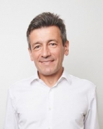
  Thomas Piliszczuk, Soitec
More than Moore with engineered substrates
Thomas Piliszczuk

Thomas Piliszczuk

Soitec

Thomas Piliszczuk

Abstract
In 1991, M. Bruel invented and patented the Smart Cut™ technology to fabricate Silicon On Insulator (SOI) substrates. The invention of this SOI process combined with the entrepreneurship of SOITEC paved the way to high quality SOI substrates mass production. Today, SOI is a mature product (up to 300mm diameter) and now developments are focused on the integration of new materials and functionalities in order to improve device performances and enlarge the application spectrum.

Biography
Dr. Thomas Piliszczuk has 30 years of experience in the Semiconductor industry. He joined Soitec in 2009 as Senior Vice President of marketing, business development and global sales. Since September 2018 he is responsible for leading Soitec’s Global Strategy. Before coming to Soitec, Dr. Piliszczuk was with KLA-Tencor, where he took various senior management positions related to business strategies and alliances with the largest semiconductor companies worldwide. During his tenure there, he had responsibility for European Operations. Earlier in his carrier, he worked at DARPA (Defense Advanced Research Projects Agency) and Sematech managing advanced lithography projects. Piliszczuk holds a Ph.D. from the Ruprecht-Karls-Universitat Heildelberg in Germany, an Electrical Engineering degree from the Gdansk Polytechnic University in Poland and an Executive Business degree from Stanford University