Tuesday, November 10, 2026
 

Start Up Pitches

13:10 Welcome Remarks by Session Chair
  Isabel Obieta, EIC Programme Manager for Responsible Electronics
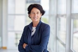
Isabel Obieta

Isabel Obieta

EIC Programme Manager for Responsible Electronics

Biography
Isabel obtained a Master Degree in Physics (Semiconductor Physics) from the University of the Basque Country (Spain) and subsequently, earned a Doctoral Degree in Science (Microelectronics-Materials for Sensors) from the University of Navarra (Spain).She started her career at AT&T Microelectronics transferred to AT&T-Bell Laboratories (USA) in the field of modelling and simulation of electronic components. Back in Spain, she joined one of the leading manufacturers of Power Discrete components, as an R&D Engineer and later, became Manager of Engineering and Production of the Wafer Fab, what gave her a wide picture of the microelectronics industry. At that position, she started her links with the European Commission as the representative of the group in Eurimus (Eureka Initiative for promotion of microsystem uses) Technical Committee.Several years later, Isabel transitioned to Project Management in the field of Materials and Microtechnologies for Electronics in the largest technology center in Spain, Tecnalia, where she has initiated, managed and coordinated several new initiatives like the Nanotechnologies Program or the Printed Electronics Platform. She has also been Director of several Business Areas leading their market-technology and IP strategy. During all those years, she has been managing a large portfolio of European and private projects in the field of Micro-Nanofabrication, Functional Surfaces, Sensors and Printed Electronics.All along her career, she has combined her job with activities as expert in innovation by performing Technology Due Diligences, evaluating new business opportunities for Venture capitals and Family offices or as Innovation Radar Expert for EU projects. She holds a title in Expert in Management of Innovation and Technology from Deusto Business School.In September 2022, she joined the European Innovation Council as Programme Manager for Sustainable Semiconductors, where she supported numerous startups and research groups in advancing their innovation pathways over a four‑year period. Since September 2026, she is working independently as a Strategy & Innovation Advisor.

13:15
Chips JU Opportunities for Start-ups and Innovation
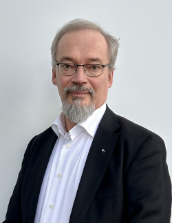

  Jari Kinaret, Executive Director, Chips JU
Chips JU Opportunities for Start-ups and Innovation
Jari Kinaret

Jari Kinaret
Executive Director
Chips JU

Jari Kinaret

Abstract
Coming Soon

Biography
Jari Kinaret was born in Finland and holds M.Sc. degrees in Theoretical Physics and Electrical Engineering from the University of Oulu in 1986 and 1987, respectively, and a Ph.D. in Physics from the Massachusetts Institute of Technology (MIT) in 1992. Prof. Kinaret has worked in various roles at research institutes and universities in Copenhagen, Denmark, and Gothenburg, Sweden. From 2013 to 2023, he served as the Director of the Graphene Flagship, a one-billion-euro research project dedicated to exploring the potential of graphene. In October 2023, Prof. Jari Kinaret assumed the role of Executive Director at Chips Joint Undertaking (Chips JU), a European public-private partnership that supports research, development, innovation, and future manufacturing capacities in the European semiconductor ecosystem.

13:30
Beyond Glass: A New Reinforcement Architecture for High-Frequency Electronics
  Andy Wynn, CEO, Flexiramics B.V
Beyond Glass: A New Reinforcement Architecture for High-Frequency Electronics

Andy Wynn
CEO
Flexiramics B.V

Abstract
As electronic systems move toward higher frequencies, increasing data rates and greater power densities, the materials used in printed circuit boards and advanced substrates are becoming an increasingly important part of system performance.Most PCB laminates continue to rely on woven glass fabrics to provide mechanical reinforcement and dimensional stability. At RF and mmWave frequencies, however, the dielectric properties of glass and its woven architecture can contribute to signal attenuation and local dielectric variation. Its relatively low thermal conductivity also limits lateral heat spreading within the laminate.Flexiramics® introduces a different approach: a flexible ceramic microfiber nonwoven designed as a reinforcement for advanced polymer composites. By replacing woven glass with a highly porous, nonwoven ceramic network, the technology aims to combine the structural role of reinforcement with electrical and thermal properties better suited to next-generation electronics.Recent material-level evaluations have demonstrated three relevant characteristics:Low dielectric loss – Flexiramics-reinforced test laminates have demonstrated 70–75% lower dielectric loss compared with 1080 glass in comparable test laminates.Improved lateral thermal conductivity – Flexiramics-based polymer composites have demonstrated in-plane thermal conductivity of approximately 2.0–2.2 W/m·K, supporting improved lateral heat spreading compared with conventional glass-reinforced systems.Nonwoven reinforcement architecture – removing the periodic woven-glass structure eliminates the glass-weave architecture responsible for local reinforcement-related dielectric variation.Together, these results demonstrate the potential of ceramic nonwoven reinforcement as a new material for high-frequency electronics.The next development stage is focused on translating these demonstrated material properties into reproducible prepregs and laminates, followed by PCB-level RF/mmWave validation and customer qualification.The presentation will introduce the Flexiramics reinforcement concept, present current material-level performance data and discuss the development pathway from ceramic nonwoven reinforcement toward qualified high-frequency PCB laminates.

Biography
Andy Wynn, PhD is CEO of Flexiramics B.V. and a technology leader with 30 years’ experience transforming new technologies into successful global businesses. Former CTO of Morgan Advanced Materials plc, $Billion FTSE 250 multinational. Brings deep expertise in aligning innovation and business strategy across industries and geographies.

13:40
The myth of troubleshooting
  Lior Messinger, CEO, Korra.ai
The myth of troubleshooting


Lior Messinger

Lior Messinger
CEO
Korra.ai

Lior Messinger

Abstract
The pitch is familiar by now: troubleshooting is what keeps tools down, and AI will finally shorten MTTR. It is a compelling story. It is also two claims stacked on top of each other, and neither has been examined closely.The first is empirical. How much of a technician's working day is actually spent troubleshooting? Measured against the full picture of setup, qualification, PM, documentation, handoffs and procedure execution, the answer is a much smaller fraction than the industry's attention would suggest. The second is a matter of judgment. Even where troubleshooting does happen, it is the worst possible place to point a probabilistic system. It is the moment with the least tolerance for a confident wrong answer, the least structured input, and the highest cost of being subtly plausible instead of correct.This talk argues that AI has been aimed at the most visible problem in the fab rather than the most valuable one, and presents an alternative: grounding AI in what the organization already knows, and separating diagnosis from procedures. We will enhance and present methods needed for real world use cases.

Biography
Lior Messinger is the founder and CEO of Korra.ai, an AI company building knowledge retrieval systems for industrial environments where the data cannot leave the building. Korra's platform runs fully on-premises and air-gapped, and is deployed in production across semiconductor manufacturing and field service operations. Lior has spent 35 years building software in high-consequence environments. He previously led physics and AI development for flight simulators and video games. He founded Korra in 2020 to let AI understand technical procedures using documentation text, visuals, and historical data.

13:50
Magnetocalorics: Next-Generation Cooling for Semiconductors

  Remi Dubois, COO, Magnoric
Magnetocalorics: Next-Generation Cooling for Semiconductors
Remi Dubois

Remi Dubois
COO
Magnoric

Abstract
Magnoric is developing a new generation of cooling systems based on the magnetocaloric effect, replacing conventional vapor-compression technology with a solid-state thermodynamic cycle.Our technology operates without refrigerant gases and combines high energy-efficiency potential with silent, vibration-free operation and reduced maintenance requirements.Magnoric has already developed and validated pre-series cooling platforms from a few hundred watts to more than 1 kW and is now scaling the technology toward higher-power applications.For the semiconductor industry, magnetocaloric cooling opens new opportunities for efficient thermal management, process cooling and heat recovery. This presentation will introduce Magnoric’s technology, its latest developments and its potential for next-generation semiconductor manufacturing applications.

Biography
Rémi Dubois is Chief Operating Officer at Magnoric, a French deep-tech company developing magnetocaloric cooling technologies. He is responsible for operations, business development and the industrialization of Magnoric’s technology, working closely with industrial partners across cooling, energy and advanced manufacturing applications.

14:00
From Plasma-System Design to Deployment: An Integrated Engineering and Global Supply-Chain ApproachSubtitle: From Process Requirements to Upgradeable Process Platforms

  Manikya Vajpayee, CEO, Aether Semiconductors
From Plasma-System Design to Deployment: An Integrated Engineering and Global Supply-Chain ApproachSubtitle: From Process Requirements to Upgradeable Process Platforms

Manikya Vajpayee
CEO
Aether Semiconductors

Manikya Vajpayee

Abstract
Session OverviewBuilding specialized semiconductor equipment takes more than process expertise; it requires coordinated system engineering, precision manufacturing, subsystem integration, and resilient supply-chain execution. This session shows how Aether Semiconductors, headquartered in India with a local engineering presence in the Netherlands, applies this integrated approach to plasma-based deposition and etch equipment for advanced- and mature-node applications.Using a representative equipment case, we show how process requirements are translated into modular system architectures spanning plasma chambers and sources, gas delivery, RF and microwave power, thermal management, vacuum systems, and controls and automation, with emphasis on system integration, interface management, qualification, and lifecycle upgradeability.We also examine how Aether’s engineering capability, combined with manufacturing and supply-chain collaboration across India, Europe, and Asia, supports adaptable plasma platforms, stronger supply resilience, faster development cycles, and long-term support.Keywords: Plasma Equipment Engineering, Global Supply Chain, System Integration

Biography
Manikya Vajpayee is the Founder & CEO of Aether Semiconductors, where he is building the next generation of scalable and upgradeable semiconductor process equipment. With over a decade of industry experience, he leads the company’s initiatives across equipment engineering, plasma process technologies, system integration, manufacturing, and global supply-chain development. His vision is to transform advanced engineering into production-ready platforms that enable the future of semiconductor manufacturing.

14:10
The Pervasive Intelligence With AI That Learns At the Source
  Enver Solan, Co-Founder & CSO, GEMESYS GmbH
The Pervasive Intelligence With AI That Learns At the Source

Enver Solan
Co-Founder & CSO
GEMESYS GmbH

Abstract
Sensors are moving into grids, vehicles, factories and wearables. They produce more data than anyone can move, store or trust to the cloud. Most edge AI deals with this through inference only: a model is trained elsewhere, compressed, and run on the device (Level 3 of edge intelligence). Adapting that model to each site, machine or user still needs cloud training, labeled data and bandwidth. Learning on the microcontroller itself is held back by memory, energy and compute. GEMESYS takes a different route. Our CMOS-compatible analog processing unit learns directly at the sensor. An event-driven analog core processes the raw signal and does the learning, while the microcontroller keeps its job and runs only a small digital layer. The goal is to complement TinyML, not replace it, and to bring existing systems to Level 6, where training and inference both happen on the device. All within a microwatt-class power budget. Early evaluations on a hardware-accurate digital twin, using real sensor data from industrial pilots, are promising. They show the potential of analog learning at the sensor for edge intelligence that is private, adaptive and light on bandwidth. Next comes silicon. We are turning the digital-twin results into silicon validation, partner evaluation kits and larger customer pilots. We are also extending the concept to new uses, such as chips that monitor their own health, performance and lifetime. The presentation will introduce Level 6 edge intelligence and the analog learning layer, share what we learned from our pilots, and lay out the path to silicon. Stop by our booth at SEMICON Europa 2026 (Hall B0) to talk it through and see the demos.

Biography
Enver Solan is co-founder and Chief Science Officer of GEMESYS, where he leads the research direction, chip development concepts, benchmarking, and the IP strategy for analog edge AI chips that make sensors intelligent and adapt on the device without a cloud connection.He studied electrical engineering and information technology at Ruhr University Bochum with a focus on communications and RF technology and received his Dr.-Ing. with distinction in 2020 for his work on the real-time emulation of adaptive circuits with memristive devices, carried out in the DFG research unit FOR 2093 on memristive devices for neural systems.Before founding GEMESYS, he worked as a systems engineer at Rheinmetall on the digitalization of land vehicles. He has published in IEEE Transactions on Circuits and Systems I and other journals and has presented at more than 20 international conferences.Further details about his professional background are available on LinkedIn https://www.linkedin.com/in/dr-ing-enver-solan-b65088137/

14:20
Forged in Orbit, Built for Earth — Space Forge's Semiconductor Strategy for Space-Grown Materials
  Markus Behet, VP BD Semiconductors, Space Forge Ltd
Forged in Orbit, Built for Earth — Space Forge's Semiconductor Strategy for Space-Grown Materials

Markus Behet
VP BD Semiconductors
Space Forge Ltd

Abstract
Compound semiconductors are moving from niche to core: the device-level market is set to double from ~$12.5 bn (2024) to ~$25 bn by 2030 (Yole), taking the sockets where physics beats cost in power, RF, photonics and quantum. Yet every compound device is only as good as the crystal it is grown on — purity, strain and dislocation density set the performance ceiling, and that ceiling is fixed long before the first lithography step. Space relaxes the dominant defect drivers. Microgravity suppresses buoyancy-driven convection and sedimentation at the growth front, enabling diffusion-controlled growth — the regime associated in the microgravity literature with order-of-magnitude reductions in dislocation density. The wake-shield vacuum of orbit reaches levels orders of magnitude beyond terrestrial growth chambers, reducing background impurity incorporation during growth. Thermally, orbit is not intrinsically stable, but the environment is predictable: purely radiative exchange against a constant deep-space sink, free of atmospheric convection, so a well-designed growth cell can be regulated precisely and repeatably. The strategic question is not whether space-grown material can be better, but how Space Forge turns that advantage into a viable semiconductor business. Space Forge (Cardiff, founded 2018; £22.6 M Series A led by the NATO Innovation Fund) answers with flight heritage and a revenue-led model. ForgeStar-1, launched June 2025, is the first commercial semiconductor factory in orbit and holds Europe's first in-space manufacturing licence; it achieved first plasma in December 2025 and has completed 100+ growth-chamber operations. The orbital payload stays in the grams range: seed crystals are grown in space, returned under the reusable Pridwen heat shield, and their superior structural quality is propagated through several iterations of terrestrial growth. Each space-grown seed yields successive generations of material produced in conventional reactors, so the economics scale on Earth while the quality is set in orbit. Space Forge’s semiconductor strategy sequences three phases on the initial diamond material platform. Phase 1: terrestrial polycrystalline diamond thermal materials, commercial today (~$150–230 M market, ~11–13%/yr) — heat spreaders for GaN RF, defence radar and power modules, a market whose millimetre-scale plates and high value per cm² fit the company's scale. Phase 2: quantum-grade single-crystal diamond substrates with engineered NV centres for quantum sensing and photonics, industrialising towards 2030. Phase 3: space-grown seeds and substrates feeding quantum computing and the most demanding sensing applications as wafer-scale diamond matures. Go-to-market is partner-led, matched to how the industry qualifies – through co-engineered demonstrators, joint qualification, committed capacity slots. Space Forge's ambition is that terrestrial revenue funds the orbital programme: start in a market whose unit economics fit the company's scale, treat flight heritage and regulatory firsts as trust assets, and keep the deepest differentiation. The Space Forge team is convinced that the next semiconductor technology will be defined by its materials, the materials by their crystals — and the quality of a crystal can be set in orbit.

Biography
I have spent 30+ years commercializing advanced semiconductor materials — following the technology curve from III-V research at imec, through GaAs RF at Siemens, Infineon and TriQuint, into the wide-bandgap era with SiC and GaN, and now to diamond and ultra-wide-bandgap (UWBG) materials.As Global Market Segment Manager at Dow Corning, I built the commercial footprint for SiC and GaN power electronics materials. As Chief Marketing Officer of EpiGaN, I helped scale the pioneering GaN-on-Si/GaN-on-SiC epiwafer supplier from start-up through its acquisition by Soitec in 2019, then led GaN Product Marketing & Business Development at Soitec as CMO of Soitec Belgium. Most recently, as Vice President Sales & Marketing EU & US for SICC, I expanded the western business of one of the world's leading SiC substrate manufacturers — recognized with the 2025 Bosch Global Supplier Award.Today, as Vice President Business Development Semiconductors at Space Forge, I lead commercial strategy for next-generation semiconductor materials: polycrystalline and single-crystal CVD diamond (PCD/SCD) for thermal management and quantum applications and further UWBG materials on the roadmap — leveraging in-space manufacturing to unlock material quality beyond terrestrial limits.What connects it all: translating materials maturity into market entry — matching the right technology, at the right point on its lifecycle, with customers whose problems it genuinely solves.

14:30 Reserved
14:40 Reserved
14:50 Reserved
15:00 Reserved
15:10 Reserved
15:20 Reserved
15:30 Reserved
15:40 Reserved
15:50 Closing Remarks by Session Chair
  Isabel Obieta, EIC Programme Manager for Responsible Electronics
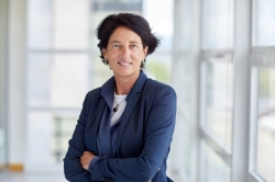
Isabel Obieta

Isabel Obieta

EIC Programme Manager for Responsible Electronics

Biography
Isabel obtained a Master Degree in Physics (Semiconductor Physics) from the University of the Basque Country (Spain) and subsequently, earned a Doctoral Degree in Science (Microelectronics-Materials for Sensors) from the University of Navarra (Spain).She started her career at AT&T Microelectronics transferred to AT&T-Bell Laboratories (USA) in the field of modelling and simulation of electronic components. Back in Spain, she joined one of the leading manufacturers of Power Discrete components, as an R&D Engineer and later, became Manager of Engineering and Production of the Wafer Fab, what gave her a wide picture of the microelectronics industry. At that position, she started her links with the European Commission as the representative of the group in Eurimus (Eureka Initiative for promotion of microsystem uses) Technical Committee.Several years later, Isabel transitioned to Project Management in the field of Materials and Microtechnologies for Electronics in the largest technology center in Spain, Tecnalia, where she has initiated, managed and coordinated several new initiatives like the Nanotechnologies Program or the Printed Electronics Platform. She has also been Director of several Business Areas leading their market-technology and IP strategy. During all those years, she has been managing a large portfolio of European and private projects in the field of Micro-Nanofabrication, Functional Surfaces, Sensors and Printed Electronics.All along her career, she has combined her job with activities as expert in innovation by performing Technology Due Diligences, evaluating new business opportunities for Venture capitals and Family offices or as Innovation Radar Expert for EU projects. She holds a title in Expert in Management of Innovation and Technology from Deusto Business School.In September 2022, she joined the European Innovation Council as Programme Manager for Sustainable Semiconductors, where she supported numerous startups and research groups in advancing their innovation pathways over a four year period. Since September 2026, she is working independently as a Strategy & Innovation Advisor.