Thursday, November 12, 2026
08:30

Arrival and Welcome Coffee


Opening Session

09:00
Welcome & Reminders
  Paul Trio, Director of Standards, Semi
Welcome & Reminders
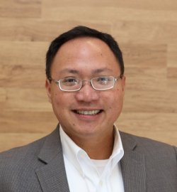

Paul Trio

Paul Trio
Director of Standards
Semi

Paul Trio

Abstract
xyzxyz

Biography
Paul Trio is Director of Standards at SEMI. Established in 1973, the SEMI International Standards Program has developed and published more than 1,100 industry-approved standards and guidelines through the contributions of more than 6,000 volunteers worldwide.Paul joined SEMI in 2002 as a Standards Engineer, supporting technical committees responsible for developing standards for factory automation, microlithography, and automated test equipment. In 2008, he assumed responsibility for North America Standards Operations.In addition to his leadership of the Standards Program, Paul collaborates with SEMI Technology Coalitions on pre-standards initiatives addressing critical industry challenges, including defect mitigation at advanced process nodes, supply chain traceability, microelectronics and systems test, electronic materials, systems integration, data interoperability, and cybersecurity.Paul holds a Bachelor of Science degree in Electrical Engineering from San Jose State University and dual master's degrees in Systems Engineering and Business Administration.

09:10
SEMI Global Standards Summit 2026"Future Standards in Focus: Innovation and Industry Readiness"
  Supika Mashiro, Advisor, Tokyo Electron Limited
Paul Trio, Director, SEMI
SEMI Global Standards Summit 2026"Future Standards in Focus: Innovation and Industry Readiness"
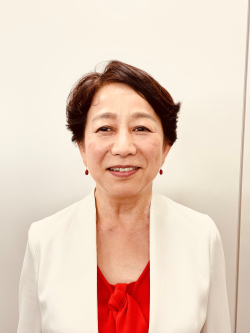
Supika Mashiro

Supika Mashiro
Advisor
Tokyo Electron Limited

List of Authors
S. Mashiro1, P. Trio2
1Tokyo Electron Limited, Technology Vision & Environment Strategy, Tokyo, Japan, 2SEMI, Milpitas, United States

Abstract
Now in its third edition, the Global Standards Summit (GSS) builds on the momentum of the past two events, providing a forum to identify potential areas for future standardization efforts.In a context of increasing complexity across the global semiconductor ecosystem, emerging technologies, regulatory requirements, and advanced research spur the need for effective standards development. The 2026 GSS will explore these current needs and contribute to shaping a roadmap for the next three to seven years.The GSS 2026 Panel discussion will explore AI in semiconductor manufacturing and its value chain and how SEMI Standard can promote AI adoption as well as be benefited from AI utilization.

Biography
With plasma etching process and equipment development engineering background, Ms. Mashiro has been active in SEMI Standards technical committees focusing on equipment-Fab integration enablers, such as EH&S, facilities, and physical interface specifications.She has been an active contributor to various SEMI EHS WGs including a leadership role in SEMI PFAS Initiative, a global technology community addressing PFAS supply chain challenges, as well as SIPS Japan regional PFAS WG.She is also active in IRDS (International Roadmap for Devices and Systems) and has been the co-chair of its Factory Integration focus team since 2016.

09:20
Bridging European Policy and Technical Standardization
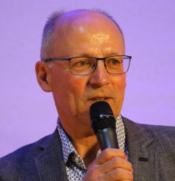
  Uwe Rüddenklau, CEN/CENELEC
Bridging European Policy and Technical Standardization
Uwe Rüddenklau

Uwe Rüddenklau

CEN/CENELEC

Abstract
coming soon

Biography
Uwe Rüddenklau is Head of Global Standardization Topics and Director of Standardization at Infineon Technologies AG, a major semiconductor company in Munich. He holds degrees in electrical engineering and marketing, and brings over 30 years of global experience in system engineering, sales, and technical marketing, particularly for RF solutions in consumer electronics and mobile applications. Uwe has held senior positions at Infineon, Lantiq, and Siemens, and actively contributes to international and European standardization bodies like IEC, ISO, CEN, CENELEC, and ETSI, where he chairs the CENELEC Technical Committee for semiconductors and trusted chips (CENELEC TC47X). Uwe is German speaker and expert in the International SDO IEC Technical committee (IEC TC47).He also engages with German government forums, standardization organizations such as DKE/VDE, DIN and industry associations such as BDI, BITKOM, and ZVEI, focusing on technical regulation and standardization for 5G, cybersecurity, and semiconductor technologies.


Session 1: Can SEMI Standards Alleviate the Impact of EU Environmental Regulations

09:45
Enabling the Transition to Mercury-Free Silicon Wafer Metrology
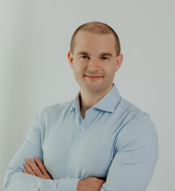

  Thomas Hager, Siltronic
Enabling the Transition to Mercury-Free Silicon Wafer Metrology
Thomas Hager

Thomas Hager

Siltronic

Thomas Hager

Abstract
The Minamata Convention on Mercury is accelerating the reduction of mercury use and creating challenges for established electrical characterization methods in the semiconductor industry. Hg-CV measurements are widely established for the characterization of bulk and epitaxial silicon, providing reliable and high precision information on carrier concentration and related electrical properties. Existing standards, e.g. SEMI MF1392 or SEMI MF723, provide an important foundation for comparable silicon wafer characterization. However, increasing restrictions on mercury drive the semiconductor industry toward reliable and sustainable Hg-free metrology solutions. New and revised SEMI standards can facilitate this transition by defining common measurement procedures, performance criteria, and correlation methods between established Hg-CV and alternative Hg-free techniques.Siltronic, one of the top five global silicon wafer manufacturers and the only Western-based manufacturer among these leading suppliers, considers advanced metrology essential for maintaining its position as a technology leader. This is particularly important for Siltronic’s strategic focus on leading-edge and power products, where reliable and accurate material characterization is crucial.Standardized qualification and correlation procedures can enable the introduction of Hg-free technologies while maintaining measurement accuracy, reproducibility, traceability, and comparability across the semiconductor supply chain. Close cooperation between wafer manufacturers, equipment suppliers, semiconductor customers, and standardization bodies will therefore be essential. International standardization of Hg-free electrical characterization can become a key enabler for sustainable, future-proof silicon wafer metrology without compromising the stringent requirements of next-generation semiconductor technologies.

Biography
Dr. Thomas Hager is Director Metrology International at Siltronic AG and holds a Ph.D. in Physics. He has extensive experience in semiconductor technology and metrology, with expertise in semiconductor laser testing and silicon wafer characterization. His professional background combines research and development of advanced testing and metrology solutions with management responsibilities. Prior to joining Siltronic, he worked at OSRAM Opto Semiconductors, where he gained experience in semiconductor laser technology and testing.

10:00
PFAS, tbc
  Supika Mashiro, GSS Committee Chair
PFAS, tbc

Supika Mashiro

GSS Committee Chair

Abstract
Abstract coming soon

Biography
Coming soon

10:20
Impact of the AI Factory on EU Enviromental Regulations
  Michael Munsey, Global VIce President Semiconductor Industry, Siemens
Impact of the AI Factory on EU Enviromental Regulations

Michael Munsey

Michael Munsey
Global VIce President Semiconductor Industry
Siemens

Michael Munsey

Abstract
Data center growth, especially as it pertains to the AI factory, is straining our energy grids and forcing countries to evaluate how to generate enough electricity to power future growth. With racks witihin data centers approaching 1MW per rack, hyper scalers are investigating how to supply enough power from the grid to the chip. EU environemtnal regulations must be considered for the future of powering data centers. The entire ecosystem is connected, from the chip to the package to the board to the blade to the rack to the data center to the grid. The entire ecosystem must be optimized and standards across the ecosystem can help optimize and allieviate the future strain on the grid.

Biography
With over 30 years of experience in the semiconductor industry, Michael Munsey leverages his extensive background in global business development, strategy, sales, and marketing to drive semiconductor technology advancements at Siemens. Before joining Siemens, he held leadership positions at several prominent companies, including Perforce where he was Senior Vice President of Marketing and Strategy and oversaw the acquisition and integration of Methodics, Dassault Systèmes where he was Vice President of the High Tech Industry and built their Semiconductor Industry, and Cadence Design Systems where he oversaw their functional verification program and introduced the Incisive verification platform. Munsey began his career in semiconductor design at IBM after obtaining degrees from Tufts University. He is actively involved in several industry groups focused on setting standards and shaping the direction of the semiconductor sector. Additionally, he is an active member and volunteer of Tau Beta Pi.

10:35

Coffee Break


Session 2: Emerging Technologies

10:50
Standards for Compound Semiconductors: Balancing Speed, Maturity, and Technical Understanding
  Siegmar Schoser, Director Cooperations, Robert Bosch GmbH
Standards for Compound Semiconductors: Balancing Speed, Maturity, and Technical Understanding

Siegmar Schoser
Director Cooperations
Robert Bosch GmbH

List of Authors
S. Schoser, H. Heinisch
Robert Bosch GmbH, Reutlingen, Germany

Abstract
Over the past five years, compound semiconductor technologies, particularly silicon carbide (SiC) MOSFETs, have gained significant market share and are expected to continue their strong growth. Driven by electrification, energy efficiency, and high-performance power electronics applications, SiC has become a key technology for automotive and industrial systems. At the same time, SiC products in 2026 and beyond remain fundamentally different from established silicon technologies with respect to product maturity, material behavior, process understanding, degradation mechanisms, and supply-chain structure. Learning cycles are still fast and not yet at the flat end of the S-curve.This creates a critical challenge for standardization. Many existing semiconductor standards were developed in a silicon-dominated environment and are not yet fully adapted to the specific characteristics of SiC and other wide-bandgap materials. Examples can be found in raw-material characterization, wafer marking (e.g. SEMI T5), defect inspection (e.g. SEMI M83-0820), and reliability validation. SiC specific standard SEMI M55 covers polished monocrystalline SiC wafers, but explicitly recognizing the weakness that additional physical, electrical, and bulk properties may be required for a complete purchase specification.Reliability validation faces a similar situation. SiC power devices exhibit additional aging and degradation mechanisms compared with silicon, including bipolar degradation and gate-related instabilities. These mechanisms are still subject to ongoing research, and mature acceleration models are not yet always available to translate mission-profile stress into robust qualification test conditions. In contrast, users have valid expectations that standards protect them from reliability risks during the expected life of a product.Even if cause-effect relations are understood by some players in the industry, particularly by implementing a good traceability from raw material to finishes goods, they might keep it confidential to gain a temporary competitive advantage. Only after several years, when multiple players have undergone the same learning cycles, this know-how gets public and can be used for the definition of standards. This slows down the development of new or the update of existing standards. At the same time, scientific contributors are lacking the required mass production experience to provide sufficient knowledge and compensate the hesitation of industrial contributors.As a result, the industry must avoid two risks: defining standards too late, which may slow global alignment, and defining overly prescriptive standards too early, which may lead to misleading test requirements, unnecessary cost, or requirements not clearly linked to real application risk.One approach to overcome this problem could be to use SEMI “Guide” documents as temporary solutions in the sense of ‘best practice’ which describes best-known-methods, provide practical direction without over-specifying immature requirements. This approach can help the industry move from shared terminology and pre-competitive engineering consensus toward durable global specifications.Standardization for emerging materials such as SiC must balance speed with technical maturity. Premature standardization can create misleading requirements, while structured pre-standards collaboration, guide documents, and traceability-based learning can accelerate the path toward robust, globally accepted SiC standards.

Biography
After graduation in physics at the University of Konstanz and obtaining a doctoral degree from the University of Augsburg, Siegmar Schoser joined the Robert Bosch GmbH in 1998. With a broad field of experience in various positions in MEMS manufacturing, automotive customer project management for parking assist systems, senior management of ECU development for door and tailgate modules as well as blower controller electronics, he joined the power semiconductor and power module area of Bosch in 2012. Today he is directing a project team on cooperation and external sourcing with a strong focus on silicon carbide related topics.

11:05
Standards for AI-enabled Factories
  Mark da Silva, Sr. Director, Manufacturing Collaborations, Semi US
Standards for AI-enabled Factories

Mark da Silva
Sr. Director, Manufacturing Collaborations
Semi US

Abstract
Coming soon

Biography
Coming soon

11:20
“Glass” as the Next Generation Compute Module Substrate - Replace silicon wafers? -
  Kishio Yokouchi, Head, Japan Jisso-Interconnect Solutions Laboratory
“Glass” as the Next Generation Compute Module Substrate - Replace silicon wafers? -

Kishio Yokouchi

Kishio Yokouchi
Head
Japan Jisso-Interconnect Solutions Laboratory

Kishio Yokouchi

Abstract
The packaging architecture of computing systems is undergoing a fundamental transition. Whereas semiconductor integration pursued monolithic System-on-Chip scaling, current AI compute modules increasingly adopt heterogeneous integration, in which multiple logic chiplets and stacked memory devices are reassembled on an interposer substrate. This shift is driven by the growing complexity of advanced IC fabrication, yield constraints, reticle size limitations, and the demand for scalable system architectures.At the same time, there's a growing need for faster and higher-capacity data exchange between compute dies and high-bandwidth memory (HBM). To achieve higher bandwidth, lower latency, and better energy efficiency, we need ultra-short, high-density connections that are closer to on-chip wiring characteristics rather than traditional package-level interconnects.Consequently, future interposer substrates must evolve beyond passive electrical redistribution layers. They will be required to provide fine-pitch electrical routing, support high-frequency and broadband signaling, and ultimately accommodate optical interconnects for energy-efficient communication at system scale.The interposer substrate that interconnects the compute die and memory requires fine, high-density wiring and bonding over the shortest distances, similar to the internal wiring of IC dies. It also needs to support high-frequency and wideband connections, including optical wiring. Regarding glass substrates, which are attracting attention as compute module substrates, we’ll discuss what should be considered in light of future changes in IC die structures and processes, as well as how to form electrical and optical active circuits on glass substrates to support optical wiring and silicon photonics.

Biography
Dr. Kishio Yokouchi is now a Head of Japan Jisso-Interconnect Solution Laboratory (J2IS), R&D consulting company. Also, he is a Visiting Professor of Materials & Surface Engineering Research Institute, Kanto Gakuin University.He received his Ph. D. in thermal management engineering from the Osaka University in 2009.He has been leading on development of electronic interconnect technologies for HPCs on 46 years. In 1979, Dr. Yokouchi joined FUJITSU Laboratories Ltd., where he has been mainly engaged in R&D on D2D interconnect technologies for supercomputers, such as the world’s first copper co-fired LTCC, Ultra-fine pitch thin film 2.5D circuit boards, and also, phase change liquid cooling technologies.From 2000, Dr. Yokouchi was the director of the Advanced Optoelectronics Technology Dept. of FUJITSU Laboratories of America Inc., where he directed R&D work on monolithic co-packaged optical integration technologies. From 2005, he has been a deputy general manager of the Device & Materials Laboratories, FUJITSU Laboratories. In 2007, He joined FUJITSU Interconnect Technologies, Ltd. (Now FICT) as a Vice president of R&D.Dr. Yokouchi has been also contributing on world major societies of electronics packaging technologies, such as IEEE EPS, IMAPS, and JIEP.He is the author or co-author of 55 technical presentations and publications, and invented or co-invented 72 U.S. and over 100 Japanese patents. He co-authored three technical books.

11:45

Networking Lunch


Session 3: Future Standards

13:00
Presenting Use Cases of Semiconductor-X Impacting the Landscape of Standards for Supply Chain Data Exchange
  Harald Gossner, Senior Principal Engineer, Intel
Stefan Benedikt, Intel
Presenting Use Cases of Semiconductor-X Impacting the Landscape of Standards for Supply Chain Data Exchange

Harald Gossner
Senior Principal Engineer
Intel

List of Authors
H. Gossner1, S. Benedikt2
1Intel, CEG PESG TEG, Feldkirchen, Germany, 2Intel, Munich, Germany

Abstract
The presentation is highlighting the use cases of traceability and sustainibility reporting like PCF which have been developed as part of the German data ecosystem project Semiconductor-X. A cross industry domain data exchange has been demonstrated and a alignment with chemical suppliers and IC customers is initiated. In the next step a global standardization is seeked to enable a seamless operation across the global semiconductor industry.

Biography
Harald Gossner holds the position of a Senior Principal Engineer at Intel. He received his diploma degree in physics from Ludwig-Maximilians-University, Munich in 1990 and his PhD in electrical engineering from Universität der Bundeswehr, Munich in 1995. For 15 years he has worked on the development of electrostatic discharge (ESD) protection concepts with Siemens and Infineon Technologies. In 2011 he joined Intel leading the system ESD robustness development for Intel products.He is the co-founder and co-chair of the Industry Council on ESD Target Levels representing more than 60 companies including all leading semiconductor manufacturers. He is President Emeritus of the EOS/ESD Association, Rome, NY, IEEE Fellow and editor of IEEE Electron Device Letters.In his role as technology advisor, he is member of the industry advisory boards of the Bavarian Government and of several Fraunhofer institutes. Since 2024 he is leading the project Semiconductor-X, coordinating the development of a dataspace for a resilient supply chain of semiconductors for Europe. He is also responsible for Intel’s activities to build-up a design ecosystem of innovative designs in digital leading edge technologies in Europe.

13:15
Future Standards for Sustainability, tbc
  Laurent Pain, Sustainable Electronics Program Director, CEA Leti
Future Standards for Sustainability, tbc

Laurent Pain
Sustainable Electronics Program Director
CEA Leti

Abstract
Coming soon

Biography
Coming soon

13:30
Future Standards for Emerging Technologies, tbc
  Ryoichi Ishihara, Delft University
Future Standards for Emerging Technologies, tbc

Ryoichi Ishihara

Delft University

Abstract
Coming soon

Biography
Coming soon

13:55 Panel discussion

Panel Discussion - AI in Manufacturing

Panelists
14:45

Wrap Up & Next Steps

15:00

Adjourn