Friday, November 17, 2023
 

Innovation Showcase

13:30
Increased use of chemical process control taking as a path to increased sustainability
  Irene Popova, Nova Ltd
Increased use of chemical process control taking as a path to increased sustainability
Irene Popova

Irene Popova

Nova Ltd

Irene Popova

Abstract
As a responsible participant in the modern economy, semiconductor industry shares a burden to Reduce, Reuse and Recycle, as much as possible. Our customers constantly feel this ever-increasing pressure but feel reluctant to fully embrace it. Simply because with it comes sharp need to balance improving process yields and device reliability, while controlling process costs, and optimizing resource utilization. Intense use of chemical materials in the semiconductor process flow is a given and often – aggressive replacement of process chemicals is a safest solution, offered in cases of process variations, unexplained process excursions. This invariably leads to massive amounts of process waste, burden shouldered by our communities and our environment. This is a perpetual challenge in our industry. So – why have not we solved it and is there a sustainable answer to this problem? We, at NOVA, believe that the answer is increased use of chemical process control. Process control not only allows to reduce natural process variation, improving overall process stability, but in case of chemical process metrology, directly translates to the reduced chemical consumption and optimized chemical lifetimes. With improved process stability and materials optimization, comes possibility to streamline chemical utilization in the fab, while maintaining process complexity, dictated by new integration schemes and material solutions. Electrochemical deposition is a particular sector, where applications at both local interconnect damascene and advanced packaging are intense chemical users, with high refresh rates and often, short bath lifetimes. At both of those instances, implementing unique solutions like DMR (Direct Metal Replenishment) or traditional chemical analyzers enables significant improvement of cost of ownership and reduction in waste generation – a win-win for the customer, environment, and process stability. Outside of the optimizing process chemicals, we believe that implementing more control solution on the incoming materials quality side allows to prevent excursions and process deviations from happening, leading to even more optimized use of resources.We will discuss several use cases where improved chemical process control by NOVA chemical analyzers shifts the scales sharply in favor of higher process yields, minimizes excursion risks while reducing the environmental impact of the semiconductor process flow.

Biography
Dr. Popova is a physical chemist and material scientist by training. She started her career at IBM Microelectronics Division in NY in 2004, where she successfully worked on developing novel types of lithographic imaging materials and their processing optimization. She has extensive experience in the semiconductor process integration and technology development side of the business both in the front and back end of the semiconductor manufacturing process. She continued her career by taking a leadership position in IBM’s advanced semiconductor packaging division in 2011, with an emphasis on R&D, before joining ancosys in 2013. Here, by engaging the team in multiple strategic collaborations, she has enabled the development of several new platforms and applications for the packaging semiconductor market, strengthening ancosys position as one of the leaders in galvanic bath inline analysis. In 2022, the company joined Nova Ltd as a chemical metrology division, and Dr. Popova now leads as a CTO in developing future applications and methodologies for chemical metrology in multiple sectors and industries.

13:45
Study of Diamond Coated Wire (DCW) slicing technique process parameters impacting high grade Semiconductor Wafer quality, mainly for Warp, Total Thickness Variation (TTV) and Nanotopology (NT)
  Carlo Zavattari, GlobalWafers
Study of Diamond Coated Wire (DCW) slicing technique process parameters impacting high grade Semiconductor Wafer quality, mainly for Warp, Total Thickness Variation (TTV) and Nanotopology (NT)
Carlo Zavattari

Carlo Zavattari

GlobalWafers

Carlo Zavattari

Abstract
The study describes in detail how the technique of slicing high grade semiconductor wafer with Diamond Coated Wire (DCW) drives mechanical wafer quality, how both the slicing process parameters and tool set-up impact the quality and how one can take advantage in tuning those parameters to properly change wafer shape according to the needs.For as cut wafers, mainly focus is on warp (warpage, wafer shape,), TTV (total thickness variation), and waviness, which is a prediction of wafer behavior at the end of the line (post polishing), where NT (nanotopology) is measured. NT is a surface variation over a small area, and it can be considered as a non-planar deviation within this area, and it can be seen as a local warp. Each of these wafer parameters are driven by different saw parameters, and the optimization of the wafer ones is descending from an equilibrium and “compromise” in the saw set-up. This means there is no optimum slicing process, but there are specific processes to fulfill different wafer requirements.The major slicing parameters are wire and coolant. Being the wire the cutting agent, its characteristics in terms of diamond grain distribution, adhesion (plating or bonding) and shape are determining the cutting ability and precision. Coolant contribution comes from its property to enhance the silicon swarf removal from the wire and the way it is distributed inside the cutting room determines the efficiency of removing not only the swarf but also the heat generated during cutting.The saw set-up includes wire management, coolant distribution, feed unit and wire guide shape. New generation saws, born in the 2010’s, have been built to optimize the DCW slicing process, which is slightly different from the slurry one (original process for wire sawing), and for some extent more critical, since the DCW is more fragile and brittle. To guarantee the proper cutting ability the new wire management needs to provide double (or more) top wire speed and acceleration compared with the past. Water and surfactant (coolant) are used instead of slurry. The coolant has a different scope compared to slurry: it is not used for cutting but for cooling and for removing the silicon swarf during cutting; thus, coolant distribution needs to be different and more focused than what is done for slurry. Feed unit and wire guide shape also need to be optimized to handle the new type of wire and its different cutting ability.This study is strictly referring to semiconductor silicon

Biography
My name is Carlo Zavattari, I have been working with MEMC Electronic Materials spa since 1995. I am an R&D senior engineer, Fellow of Global Wafers company.I am primarily working in slicing silicon wafers for semiconductors, developing new techniques to improve wafer quality.. My career has been developed at Corporate level, working on new processes in Europe, Far East and US.This paper represents the development of about 15 years of slicing silicon wafers with the diamond coated wire technology.This is a brand new edition of the article, which is submitted for the first time.

14:00
Adding Automation (SECS/GEM) Capabilities on Legacy Equipment

  Nirav Thakkar, Einnosys Technologies
Adding Automation (SECS/GEM) Capabilities on Legacy Equipment
Nirav Thakkar

Nirav Thakkar

Einnosys Technologies

Nirav Thakkar

Abstract
OverviewSEMI's SECS/GEM standards have become the de-facto communication protocol for semiconductor equipment to interface with factory systems. These standards prevent human errors in selecting incorrect recipes and enable equipment performance monitoring. However, many smaller fabs and assembly, test, and packaging factories still have legacy equipment without SECS/GEM capabilities. Adding SECS/GEM functionality to such equipment has posed challenges due to discontinued OEM support and expensive upgrades. This hinders factories from achieving improved yields, cycle times, and automation benefits.Plug-n-Play SECS/GEMTraditionally, SECS/GEM capability must be purchased from the OEM and integrated at the source code level. Some companies offer "black box" solutions, but they have limitations and potential side effects. A better approach is using equipment PC peripherals to add SECS/GEM capabilities. Data can be extracted from the equipment's controller GUI using computer vision and AI technologies, and remote control commands can be sent through the equipment PC's mouse and keyboard interface.Enhanced Automation CapabilitiesThe peripheral-level approach allows for safer integration without side effects. Additionally, AI/ML and computer vision technologies can enhance automation capabilities beyond SECS/GEM standards. This includes sending images of wafer measurements or inspections, enabling Robotic Process Automation (RPA) on the equipment, and allowing remote desktop access to equipment without a network connection. Implementing this approach overcomes challenges associated with legacy equipment and unlocks automation benefits.

Biography
Nirav Thakkar is a highly accomplished professional with a diverse background in software engineering and business administration. He received his Bachelor of Computer Engineering degree from the University of Mumbai, India in 1994, and later pursued an MBA from Pepperdine Graziadio Business School in Los Angeles, CA, which he successfully completed in 2012.He has gained valuable experience throughout his career, working in various roles and organizations:Software Engineer at Symmetric Multiprocessing (1995 - 1996):During his one-year tenure at Symmetric Multiprocessing, He contributed as a Software Engineer, utilizing his technical skills to develop software solutions.Project Lead at Contech Software Ltd (1996 - 1999):He took on the role of Project Lead at Contech Software Ltd, where he demonstrated leadership abilities and successfully managed projects for a span of three years.Senior Factory Automation Engineer at Conexant (1999 - 2002):In this position, He focused on factory automation engineering, utilizing his expertise to optimize and improve automation processes during his three-year tenure with Conexant.Software Development Manager at Oraxion (2002 - 2003):As a Software Development Manager at Oraxion, He assumed responsibilities for managing software development projects, overseeing teams, and ensuring successful project outcomes.Project Lead at Wonderware Invensys (2004 - 2006):He served as a Project Lead at Wonderware Invensys, where he led and coordinated projects for two years, leveraging his skills to deliver high-quality software solutions.VP - GLA - LIG - Ventura County at itSMF (2010 - 2011):He held a leadership role at itSMF as VP - GLA - LIG - Ventura County, contributing to the organization's goals and initiatives during his one-year tenure.Senior Engineering Manager (Factory Automation/Software Development) at Skyworks Solutions Inc (2006 - 2013):During his seven-year tenure at Skyworks Solutions Inc, He played a crucial role as a Senior Engineering Manager, focusing on factory automation and software development. He demonstrated his leadership abilities and contributed significantly to the company's success.In addition to his professional roles, He is also an entrepreneur and a founder. Since 2013, he has been the Founder and President of eInvenSys Technologies, a company that specializes in providing innovative technological solutions. Moreover, He is also the Founder and President of eInnoSys Inc, a company he established in 2013, which focuses on driving innovation in the industry.With his extensive experience and entrepreneurial spirit, He continues to make valuable contributions to the field of software engineering and technology.

14:15 Reserved
14:30
Energy-Efficienct Compute For A Sustainable Future

  Gaurav Gupta, VP Analyst, Gartner
Energy-Efficienct Compute For A Sustainable Future
Gaurav Gupta

Gaurav Gupta
VP Analyst
Gartner

Gaurav Gupta

Abstract
Energy consumption is one of the most relevant issues for information and communication technologies (ICT). New workloads for compute-heavy simulations/forecasting are demanding performance increases that can be achieved only with increasing levels of parallelism (and, hence, power consumption) to deliver the required capabilities. With emerging large language model (LLM) applications, such as generative AI, that require massive workload clusters, this challenge will only become a bigger concern. With worldwide ICT energy demands increasing at a rate higher than global electricity production, resources for generating electricity will feel the pressure. Hence, ICT energy consumption is becoming a key issue for a sustainable future.For more than 50 years, the semiconductor industry has managed to maintain the cadence of Moore’s Law for improvements in integrated circuit performance, and it has driven computing costs (performance per watt) down. That is all changing. Over the past 10 years or so, the cadence of Moore’s Law has slowed down, with the result that the semiconductor industry can no longer deliver improvements in device scaling and power efficiency at historical rates. This presentation will focus on various innovations in the semiconductor industry for energy-efficiency compute to ensure a sustainable future.

Biography
Dr. Gaurav Gupta is a VP Analyst in the Emerging Trends and Technologies team at Gartner. Dr. Gupta's research areas include semiconductor manufacturing process, chip design trends, AI analytics in chip manufacturing, and chip industry economics and supply chain. Dr. Gupta also covers emerging areas, such as autonomous vehicles, Quantum Computing, and energy efficient compute technologies for a sustainable future.Prior to joining Gartner, Dr. Gupta worked as a Knowledge Expert at McKinsey & Co. where he advised clients across the globe in the semiconductor and electronics industry with a focus on business transformation (cost, operations, and growth) and product strategy (launch/development/planning). He has a strong technical background in the semiconductor industry in process, yield, R&D, and integration, having worked at Intel, IBM and GlobalFoundries prior to the stint with McKinsey & Co. Dr. Gupta has delivered keynote speeches at several forums and conferences on a broad range of topics.

14:45
Ai-Based Defect Classification: an Accuracy and Efficiency Boost

  Bart Van Poucke, Robovision
Ai-Based Defect Classification: an Accuracy and Efficiency Boost
Bart Van Poucke

Bart Van Poucke

Robovision

Abstract
The growing complexity of Integrated Circuit (IC) architectures poses a challenge for accurate imaging and detection of defects. Furthermore, the shift towards high-mix low-volume production schemes presents challenges for cost-effective automated inspections. Although the introduction of Automatic Defect Classification (ADC) solutions mitigates the heavy load on human resources in fabrication, there remains an application mismatch between low classification accuracy and the high purity needs. The presented Deep Learning AI-based classifier increases accuracy (intelligence) in defect classification for both existing and newly-found defect types from an assortment of wafer designs.During semiconductor manufacturing, classifications that do not meet the required confidence level (class threshold) for a specific class will be labelled as “Unknown” and are presented to the operator for manual classification.The result is a continuous refinement of the model providing higher classification accuracy over a broader range of class types. An ADC solution is no different than any other tool on the manufacturing floor. Just like an etcher or a polisher, ADC executes a recipe and produces a result. The AI-ADC solution is built with an intuitive UI designed to guide you through the natural steps of collecting/managing samples, configuring image detection, setting up classifiers, and verifying the results. The biggest difference versus training a human however, is that you only need to train a single ADC system, as opposed to a small army of human reviewers.Defects in the complex chip manufacturing process are specific to the process layer and may depend on the particular IC being fabricated. As such, recipes should either be capable of handling the variation, or they should be customised to the specific layer or specific IC. Rule-based ADC struggles to generalise defects over ICs and process layers due to its nature and consequently requires a consistent customisation effort by highly skilled specialists.In the process of manufacturing chips, different layers of interconnects in the Back End Of Line (BEOL) can have distinct design rules that result in varying dimensions of defects. However, the characteristics of the defects themselves are comparable across the different layers. Consequently, AI-based recipes can be generalised across multiple layers and multiple ICs, which can significantly increase the efficiency of recipe creation and tuning.

Biography
Bart has built up experience in the semiconductor industry at imec where he was leading advanced research programs for buillding applications in using advanced technology nodes. Later he took up a Product Management leadership role at ST Engineering iDirect. Now he is combining these experiences at Robovision as responsible for developing new vision AI application in the semiconductor market.

15:00
Manufacturing next generation power devices – how temporary bonding allows wide bandgap power devices to go vertical.

  Elisabeth Brandl, EVG
Manufacturing next generation power devices – how temporary bonding allows wide bandgap power devices to go vertical.
Elisabeth Brandl

Elisabeth Brandl

EVG

Elisabeth Brandl

Abstract
Wide bandgap power devices are experiencing a strong growth, especially SiC and GaN technologies are in the front seat. Reason for that growth are mainly electronic vehicles and renewable energy but also the general need for efficient, low loss power conversion. However, both SiC and GaN still face challenges. For SiC the transition to 200mm wafers is still not implemented in the extent to satisfy industry’s demand. GaN is facing technological challenges where only lateral devices with a therefor limited breakthrough voltage are commercially available yet. A novel approach is the transition to vertical devices where a higher breakthrough voltage and therefore wider application window can be expected.For better thermal management temporary bonding was already implemented for lateral GaN power devices, but for vertical GaN power devices grown on foreign substrates, temporary bonding is an essential and critical block in the manufacturing chain.SiC power devices on small wafer sizes not necessarily need temporary bonding as mechanical support during thinning because of SiC’s robust nature. Going to 200 mm wafers temporary bonding is also a necessary process enabling thinning and backside processing.In the presentation the different process flows for wide bandgap power devices with their unique challenges will be discussed and an outlook on the manufacturability on future devices will be given – a focus will be the process compatibility of the temporary bonding during growth substrate removal for GaN power devices and thinning for SiC power devices as well as metal contact formation will be reviewed.This project has received funding from the ECSEL Joint Undertaking (JU) under grant agreement No 101007229. The JU receives support from the European Union’s Horizon 2020 research and innovation program and Germany, France, Belgium, Austria, Sweden, Spain, Italy.

Biography
Elisabeth Brandl is product marketing manager at EV Group for temporary and adhesive bonding and works for EVG since 2014. She holds a Master degree (DI) in technical physics from the Johannes Kepler University Linz specialized on nanoscience and - technology. During her master thesis at the institute of semiconductor and solid state physics she gained experience for semiconductor processing and nanofabrication.

15:15
Enabling smart manufacturing and new processes for fab automation – Equipment control tools for longer machine lifetime and material rescue
  Natalie Schulze, Product Manager Equipment Control and Integration, Kontron AIS GmbH
Enabling smart manufacturing and new processes for fab automation – Equipment control tools for longer machine lifetime and material rescue
Natalie Schulze

Natalie Schulze
Product Manager Equipment Control and Integration
Kontron AIS GmbH

Natalie Schulze

Abstract
Special tools in the software equipment control can help prevent failures, step in sooner or limit the damage. Depending on type of failure and the wafer and tool type, the overall damage value can reach up to hundreds of thousands of dollars.The efficient management and monitoring of equipment play a vital role in minimizing downtime, reducing maintenance costs and maximizing productivity. Equipment control software provides an array of functionalities, including real-time monitoring, predictive maintenance, and intelligent decision-making capabilities, all of which contribute to prolonging the lifespan of machines and enabling effective material rescue.To ensure longer machine lifetimes, equipment control software offers real-time monitoring capabilities that allow operators to track the performance and condition of machines continuously. By analyzing data collected from various sensors and components, potential issues and anomalies can be detected at an early stage, enabling proactive maintenance interventions. Timely identification of impending problems helps prevent major breakdowns and costly repairs, ultimately increasing the overall lifespan of machines.Moreover, equipment control tools incorporate predictive maintenance features that utilize advanced algorithms and machine learning techniques. These capabilities enable the software to analyze historical data, predict future failures or malfunctions, and recommend optimal maintenance schedules. By implementing preventive measures based on these insights, organizations can minimize unexpected downtime, reduce maintenance costs, and extend the operational life of their equipment.Another crucial aspect of equipment control software is its ability to support material rescue efforts. In manufacturing processes, scraps, or defects often occur. By leveraging intelligent decision-making capabilities, equipment control tools can identify salvageable materials, redirecting them for reuse or repurposing. This not only helps reduce material waste but also promotes sustainability and cost-effectiveness within production cycles.To address the security concerns, a set of recommended security measures that should be integrated into equipment control systems compliant with E187 and E188 is also necessary. These measures encompass various layers of defense, including network security, access controls, encryption, intrusion detection systems, and incident response mechanisms. Moreover, it emphasizes the importance of ongoing monitoring, vulnerability management, and security awareness training for personnel involved in equipment control system operations.In conclusion, equipment control software plays a critical role in optimizing equipment performance, prolonging machine lifetimes, and facilitating material rescue. Real-time monitoring, predictive maintenance, and intelligent decision-making capabilities all contribute to achieving these goals. By implementing these tools, organizations can ensure efficient operations, minimize downtime, and contribute to a more sustainable and cost-effective and secure SEMI compliant manufacturing ecosystem.

Biography
Natalie Schulze is Product Manager for SEMI compliant Equipment Control and Integration Software at Kontron AIS GmbH in Dresden. Before joining the Kontron team in 2022, she worked in the Machine Vision industry for Baumer, managing all Vision Technologies related accessories, including calbes, lenses and illumination supporting automation.

15:30
Enabling smart manufacturing in semiconductor fabs using predictive design and process insights
  Srividya Jayaram, Siemens Digital Industries Software
Enabling smart manufacturing in semiconductor fabs using predictive design and process insights
Srividya Jayaram

Srividya Jayaram

Siemens Digital Industries Software

Srividya Jayaram

Abstract
As semiconductor fabrication pushes the boundaries of physics and chemistry, machine learning (ML) is sought to tackle complex design and process interactions. For advanced nodes, robust process control is essential early in development cycle due to the complexity of the process flow. Additionally, during the first stage of a new product introduction (NPI) in the fab, design validation is a crucial step with only minimal margin of allowed error. Rapid advancements in ML and availability of big data have allowed semiconductor fabs to analyze large amounts of both design and fab data, to make informed decisions and enhance processes through pattern and trend identification. In this talk, we will present the details with results on using Calibre® Fab Insights tool to enable smart manufacturing in three major applications areas within the fab, that can ultimately help in accelerating the yield ramp. First area is process monitoring (PMON), where we leverage usage of design and process features to prescribe product dependent process adjustments which in turn help accelerate NPI, improve automated process control (APC), provide actionable insights to identify parameters that most impact any given process step. The second area is tool monitoring (TMON), where the ML model can help early detection of tool drifts, that cause tool to go out of control (OOC), by providing alerts to perform a predictive maintenance. This can reduce the process/tool tuning time to bring them back to spec after a preventive maintenance (PM) cycle. The final area of application highlighted is virtual cross metrology (CM) where a digital metrology twin is created that enables prediction of metrological measurements at every intermediate step along with wafer maps. Additionally, root cause analysis (RCA) to highlight non-intuitive and overlooked parameters that systematically may contribute to yield results can be obtained. These applications and use cases pave the way to use smart manufacturing concepts to decouple, isolate and quantify the individual influences each step in the fab imposes on different products at various stages of the fabrication flow. This ultimately helps provide an accelerated yield ramp curve that translates into cost and time savings.

Biography
Srividya Jayaram is the Principal Product Engineering Manager for the Wafer Defect Management solutions and Fab Insights products under Calibre semiconductor manufacturing software tools at Siemens EDA. She currently leads the joint product engineering and marketing efforts for Fab analytics domain, researching practical EDA solutions to challenges identified in the Fab. She joined Mentor Graphics in 2005 (acquired by Siemens in 2017) and held various product engineering and technical marketing roles in OPC and RET areas. Sri has over 30 publications and is actively involved in the SPIE and SEMI activities. She received her B.S. degree in electronics and communications engineering from University of Madras, India and Masters in electrical engineering from State University of New York at Buffalo in 2005.

15:45
Cost-Efficient Wafer-level SOI Process for Thermal Stability and Area Shrinkage in 3D NAND Peripheral Circuit
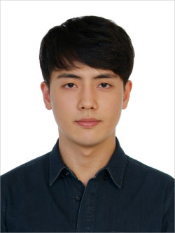
  Seungmin Lee, Sungkyunkwan University
Cost-Efficient Wafer-level SOI Process for Thermal Stability and Area Shrinkage in 3D NAND Peripheral Circuit
Seungmin Lee

Seungmin Lee

Sungkyunkwan University

Abstract
In this study, we propose a low-cost implementation of silicon-on-insulator (SOI) through wafer-level processing. In the foundry industry, the FDSOI technology, which was once in competition with bulk FinFET, is currently used only in limited technology nodes due to its high wafer unit price. Using the proposed process integration, SOI can be achieved with just the addition of one photo mask, effectively solving the cost problem, which is the main drawback of SOI. However, this technology is implemented by removing the sacrificial film through the shallow trench isolation area and replacing it with an insulator, which results in the need to consider process margins during the layout design stage. Therefore, rather than using it in a foundry where design and process are separated, it is appropriate to use it for a memory device that is easy for DTCO as the design and process are conducted in one company.Considering these factors, we aim to utilize the proposed SOI technology in the peripheral circuit of 3D NAND. In the era of big data, NAND Flash, which traditionally served as a storage device with relatively low I/O speed, now faces increasing demands for higher I/O speeds. The cost-effective SOI presents a promising alternative in this regard. Particularly in 3D NAND, where the cell process occurs after the formation of the peripheral circuit, the high thermal budget during cell processing can negatively impact transistor performance and pose challenges for achieving high I/O speeds. By utilizing SOI, a thermally robust peripheral circuit can be realized, as the insulating film beneath the single-crystal Si acts as a physical barrier, preventing dopant thermal diffusion. The stability of the thermal budget was verified through dopant diffusion TCAD simulations, evaluating parameters such as DIBL and subthreshold swing, under high-temperature and prolonged annealing conditions.Furthermore, SOI offers effective scaling of the peripheral area. Because the program-and-erase operation of 3D NAND requires a high voltage of 20 V or higher, a charge pump with a large area is required. Additionally, as 3D NAND is stacked, the parasitic capacitance between WLs and that between the WL and the string increases. As a result, the area of the charge pump tends to increase. The top Si, insulator, and Si bulk structures can be formed in parallel beneath the existing MOS and MIM capacitors, resulting in a potential capacitance increase of up to 41% within the same area.

Biography
Seungmin Lee received the B.S. degree in computer and communication engineering from Korea University, Seoul, South Korea, in 2016. In the same year, he joined Samsung Electronics Company Ltd., Hwasung, South Korea, and is currently working as a Staff Engineer in the Flash memory development division. Additionally, he is currently pursuing the M.S. degree in semiconductor and display engineering at Sungkyunkwan University, Suwon, South Korea. His current research focuses on next-generation DRAM and Flash memory architecture.

16:00
Building A More Sustainable CuCMP Process: Selective Copper Removal & Recovery
  Cameron Lippert, ElectraMet
Building A More Sustainable CuCMP Process: Selective Copper Removal & Recovery

Cameron Lippert

ElectraMet

Abstract
Challenge: (1) Current Cu-CMP processes are unsustainable due to the large amounts of waste copper that end up in the wastewater, millions of kgs per year combined (2) Complicated wastewater matrix makes treatment to remove copper to meet discharge compliance burdensome and expensive, (3) Evolving Cu-CMP chemistries that produce copper laden wastewater that is unable to be treated with conventional treatment solutions. Urgency: (1) Pressure to meet ESG targets of recycling water and waste as well as decarbonization, (2) Copper demand outpacing supply and Cu-CMP produces a large amount of recoverable copper waste, (3) Increasing cost to treat more complex CMP slurry matrices, (4) Current solutions for treatment rely on chemistry or consumable media which are subjected to an unpredictable supply chain.Solution: Electrochemical device (chemical-free) to selectively remove AND recover copper form complex streams without damaging the slurry mixture.ElectraMet® is an electrochemical system for targeted metals removal from process and wastewater streams. This system uses an automated process to treat CuCMP rinse/wastewater directly at the customer site by removing and recovering Cu as high purity metal sheets while achieving discahrge limits (sub mg/L) in the wastewater. This process leaves the rest of the slurry mixture in tact potentially allowing the slurry mixture to be reused. By electrochemically recovering copper, ElectraMet has proven to be a simple and efficient on-site solution for CuCMP wastewater treatment, even in the presence of other chemicals. ElectraMet does not rely on chemicals for its treatment, the overall operation is simpler, and the footprint is much smaller, than other on-site options.ElectraLink™ is an assurance program that provides an additional layer of support by allowing ElectraMet engineers to monitor your system on your behalf in real time. ElectraLink uses a secure cellular connection to run remote diagnostics, send daily system reports, and can protect you from costly downtime. With ElectraLink, historical trends and changes to the water treatment process can be tracked in real-time including monitoring of alarm codes, tank levels, pressure drops, valve positions, pH, and ElectraMet cartridge diagnostics. The ability to actively monitor these process conditions means you can avoid possible upset conditions that result in tank overflows, lack of proper water treatment or impurity removal, or flow-limiting pressure conditions.

Biography
Dr. Cameron Lippert is the Co-Founder, and Chief Innovation Officer at ElectraMet. Dr. Lippert is a serial entrepreneur with over a decade of experience in developing innovations and bringing them to market. In this role, he is responsible for identifying and developing new industry applications for ElectraMet. He is also in charge of identifying key product development needs to solve evolving industrial process water and wastewater challenges. Prior to becoming an entrepreneur, Cameron managed multimillion dollar R&D and technology development & demonstration projects at the Center for Applied Energy Research at the University of Kentucky ranging from carbon capture to new battery chemistry.Dr. Lippert received his BS in Biochemistry from Eckerd College and a Ph.D. in Inorganic Chemistry from the Georgia Institute of Technology, and has more than 50 publications and patents in the field.

16:15
Future of Computing: Silicon-based Quantum Computing Processors
  Himadri Majumdar, Chief Executive Officer and co-Founder, SemiQon
Future of Computing: Silicon-based Quantum Computing Processors
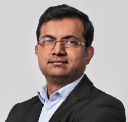
Himadri Majumdar

Himadri Majumdar
Chief Executive Officer and co-Founder
SemiQon

Himadri Majumdar

Abstract
SemiQon develops silicon-based quantum processors that will facilitate the scalability, sustainability and affordability of quantum computers. SemiQon's processors are manufactured using semiconductor fabrication processes in a foundry, suitable for mass-manufacturing. This allows SemiQon to build it's processors with scalability aspect in-built, which allows the manufacturing of million of qubits in future. That is the estimate of necessary qubits for error-corrected quantum computing for practical applications in future.In this presentation at the future of computing session of the Semicon Europa event we will introduce SemiQon's solution in more details. SemiQon was recently awarded an European Innovation Council Transition grant, together with it's partner Qblox, worth 2.5M€. In the presentation we will also breifly introduce the project, named Scallop, and its goals.With the current Chips Act initiative in Europe the goal is to reach technological sovereignty with semiconductor manufacturing in future. SemiQon's quantum processors pave the path for such sovereignty in the quantum computing industry, an industry where Europe is a global leader, and will further strengthen Europe's position during the sclability growth phase of the industry in future.

Biography
Himadri Majumdar is the Co-founder and Chief Executive of SemiQon. Prior to co-founding SemiQon he was the Program Manager for Quantum Technologies at VTT Technical research Centre of Finland. In that role he helped companies in quantum technology domain - especially fabless start-ups - to utilize VTT’s R&D expertise and infrastructure in quantum technologies. Himadri was also a founding member of the Finnish Quantum technologies ecosystem, InstituteQ, and led the business arm of the ecosystem, BusinessQ. Himadri led the European Quantum technology pilot line initative, named Qu-Pilot, with 20+ partners and 19M€ budget before he moved to SemiQon. Himadri has 20 years of experience in innovation and innovation management and is also trained as an experimental physicist. More details about Himadri's professional career can be obtaind from Linkedin [https://www.linkedin.com/in/himadrimajumdar/]