Tuesday, November 14, 2023
 

Integrated Photonics

15:10 Opening Remarks by Session Chair
  Gabriel Kittler, Chief Executive Officer Site Erfurt, X-FAB Semiconductor Foundries GmbH
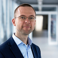
Gabriel Kittler

Gabriel Kittler
Chief Executive Officer Site Erfurt
X-FAB Semiconductor Foundries GmbH

Biography
Dr. Gabriel Kittler is Managing Director of X-FAB Semiconductor Foundries GmbH in Erfurt (Germany). He started his professional career at X-FAB in 2007 in the area of process development and became Innovation Manager from 2012 to 2020. He studied electrical engineering and information technology at the Technical University of Ilmenau from 1998 to 2003, specializing in microelectronics and sensor technology, and subsequently completed his PhD thesis in 2007.

15:15 Overview Integrated Photonics, Ivan Nikitski, EPIC
15:35
VCSELs - Development - Production - Market
  Roman Koerner, Head of global R&D (CTO), TRUMPF
VCSELs - Development - Production - Market
Roman Koerner

Roman Koerner
Head of global R&D (CTO)
TRUMPF

Roman Koerner

Abstract
In this presentation TRUMPF will sketch the latest technology of the worlds smallest and most commercialized light source - the VCSEL (vertical cavity surface emitting laser). With an annual volume of more than 2 billion devices, the production technology of III-V semiconductors on 6" has its own challenges and found ways beyond what is known in Silicon. The next generation of VCSEL devices will also require a more advanced production and packageing tool set to fullfill the demands of sensors and datacom applications in the future. If the Silicon-Industry goes 3D is the VCSEL industry ready to follow up this trend ?

Biography
Dr.-Ing. Roman Körner is the head of global R&D (CTO) and responsible for all VCSEL related technology.

15:55
Photonic IC Design: Innovation and Scalability
  Pieter Dumon, CTO, Luceda Photonics
Photonic IC Design: Innovation and Scalability

Pieter Dumon
CTO
Luceda Photonics

Abstract
Photonic integrated circuits are steadily growing in scale from just 5-10 integrated components to hundreds, as well as in number of process steps and materials. Because of the breadth of the application space, numerous material and process platforms serve different submarkets. To increase IC complexit, re-use and addressable markets, heterogenous integration of dies and chiplets of different optical materials is becoming a market reality.There is an equal diversity in the maturity level of the photonic IC technologies. Device design, compact modeling, circuit analysis, placement and routing and verification all require tools and algorithms specific to the physics as well as application requirements of phtoonic ICs. We will discuss recent technology innovations in photonic design automation technology of photonic ICs to address the above scaling challenges.

Biography
Pieter Dumon is CTO of Luceda Photonics, which he co-founded in 2014 as a spin-off from Ghent University, imec and VUB. He obtained his EE MSc degree in 2002 and a PhD in photonics in 2007 with work on silicon photonic wavelength filters. Pieter coordinated ePIXfab, the first multi project wafer service for photonics from 2007 until 2014, where he extended the collaboration to include more technology providers as well as design and packaging providers. At Luceda Photonics, he is responsible for R&D and leads the PDK team that manages over 30 photonic design kits of more than 20 photonic foundries.

16:15
How PICs fit in a Heterogeneous World
  Frans Scheper, Supervisory Board Member PhotonDelta, Former President & General Manager EMEA Intel Corporation, PhotonDelta
How PICs fit in a Heterogeneous World
Frans Scheper

Frans Scheper
Supervisory Board Member PhotonDelta, Former President & General Manager EMEA Intel Corporation
PhotonDelta

Frans Scheper

Abstract
Photonic Integrated Circuits (PICs) use photons instead of electrons to sense, process and transmit data at unparalleled speed & sensitivity. In combination with electronics, these circuits enable the creation fast and energy-efficient devices, adding new functionalities that push the boundaries of innovation. A combination of platforms is needed to unlock the full potential of photonic chip technology, as each platform has characteristics that in combination can unlock the desired functionality for new applications. Next to Silicon Photonics, Indium Phosphide and Silicon Nitride are gaining in popularity as Indium Phosphide (III/V) can integrate active components such as lasers, amplifiers and detectors on the wafer and Silicon Nitride can process visible light with very low losses. To unlock the full potential of integrated photonics, the platforms need to work together. However, blending these different elements onto a chip can be challenging when producing in high volume. With strong support from the government and industry, PhotonDelta is looking for international collaboration to achieve the ambitions depicted in the National Growth Fund Programme – a €1,1 billion programme to accelerate the PIC industry. This presentation will give an overview of the latest trends & developments and provide insights into the future of the European ecosystem for integrated photonics. It also points out the challenges and calls for collaboration with the semiconductor community to reach high volume production of photonic chip technology, creating new applications, opening the door to new markets.

Biography
Frans Scheper is a Member of the Supervisory Board of PhotonDelta, a growth accelerator for the photonic chip industry based in the Netherlands. Prior to joining PhotonDelta, Frans was Corporate Vice President and President for Europe, Middle East, and Africa (EMEA) for Intel Corporation. He was responsible for Intel's overall business in EMEA and also in charge of overseeing Intel's IDM 2.0 strategy across Europe, with research, design, leading-edge semiconductor manufacturing. Prior to Intel, Frans was Chairman and Executive Vice President of Opto Semiconductors at ams OSRAM, and has also held executive board positions at WeEn Semiconductors, NXP Semiconductors, and was the CEO and President at Nexperia Semiconductors.

16:30
Germanium Substrates for Photonics: GaAs Replacement Advantages and New Production Possibilities through CMOS Integration
  Ivan Zyulkov, Business Development Manager, Umicore
Germanium Substrates for Photonics: GaAs Replacement Advantages and New Production Possibilities through CMOS Integration
Ivan Zyulkov

Ivan Zyulkov
Business Development Manager
Umicore

Ivan Zyulkov

Abstract
Fast growth of consumer and automotive markets drives developments of new photonic devices such as micro-LEDs, multi-junction VCSELs and imagers both in the NIR and SWIR spectrum. While most of the photonics devices produced today are manufactured using GaAs substrates as a platform, there are more and more developments showing advantages of using Germanium (Ge) over GaAs. In this presentation we are focusing on technical advantages of using Ge, explain nuances of epitaxial growth on Ge substrates such as auto-doping effects and anti-phase domains and how to avoid them. In addition, we are going to discuss in more details the environmental and financial benefits of performing Ge substrate recycling for volume applications.Another aspect of photonics device manufacturing is processing of epitaxially-grown wafers into functional devices. While most of the photonics devices are manufactured by traditional III-V IDMs and foundries, cutting edge photonic chips could be made in close collaboration between III-V companies and Silicon semiconductor / CMOS players in order to improve a form-factor, device performance and to drive down production costs. This possibility is currently limited by GaAs wafer size and CMOS fab contamination requirements. Umicore works on 8’’ and 12’’ Ge substrates that can serve as a bridge between III-V world and Semiconductor industry due to the size and Germanium material compatibility with CMOS specs. In this presentation we are going to present our roadmap to CMOS compatible Ge wafer development.

Biography
Ivan currently serves as a Business Development Manager at Umicore, where his focus lies in Germanium-based materials for the photonics market. He specializes in Vertical-Cavity Surface-Emitting Lasers (VCSELs), Light Detection and Ranging (LiDARs), and Augmented Reality/Virtual Reality (AR/VR) technologies.Before joining Umicore, Ivan gained substantial experience in the field of microelectronics, having worked at multiple companies including ASM International and IMEC.Ivan holds a PhD in Chemistry from KU Leuven in Belgium. His research, undertaken at IMEC, revolved around exploring various techniques for metal deposition in microelectronics.

16:50
PhotonixFAB – The EU-funded Pilot Line to Empower Photonics Innovations
  Joni Mellin, BL manager photonics, X-FAB Semiconductor Foundries GmbH
PhotonixFAB – The EU-funded Pilot Line to Empower Photonics Innovations

Joni Mellin

Joni Mellin
BL manager photonics
X-FAB Semiconductor Foundries GmbH

Joni Mellin

Abstract
photonixFAB project aims to empower photonics innovation by SMEs and large entities by providing low barrier access to both low-loss silicon nitride (SiN) and silicon-oninsulator (SOI) based photonics platforms with indium phosphide (InP) and lithium niobate (LNO) heterogenous integration capabilities. Project objective is to establish a European photonics device value chain and initial industrial manufacturing capabilities. Thus, providing a path to scalable high-volume manufacturing for innovative product developers. This will strengthen the continent’s manufacturing capabilities in key emerging areas.

Biography
Joni Mellin has acted as Photonics product marketing / business line manager at X-Fab since 2022. He joined X-FAB from ams OSRAM, where he held Engineering director and other positions in the Full Service Foundry division since 2014. Prior to that, he held managerial and R&D positions at Microsoft, Nokia, Micro Analog Systems and VTI technologies. Joni Mellin helds Licentiate of Science and Master of Science degrees in semiconductor technology from the Aalto University and a dual Global Executive MBA degree from WU Vienna and University of Minnesota

17:10
PICs for Alternative Computing Discourses
  Madhav Pulipati, Chief Executive Officer, Photonics Valley Corporation
PICs for Alternative Computing Discourses

Madhav Pulipati

Madhav Pulipati
Chief Executive Officer
Photonics Valley Corporation

Abstract
The world is evolving into a plethora of ‘Alternative computing paradigms’, in the backdrop of ‘Beyond Moore’ scenario. Photonics, Quantum and Neuromorphic computing, among others, started positioning themselves as the plausible future computing discourses. Having established in the communications space, Photonics started offering solutions in the computing space. Integrated Photonics is the order of day and PICs lead the way forward. Among several various applications, Integrated Photonics are decisively providing valuable propositions for the Quantum discourse in such a way that the discipline of ‘Quantum Photonics’ started assuming prominence. PICs, specifically started extending tremendous advantages in the space of Quantum communications and Quantum computing. The presentation focuses on the trends of Integrated Photonics with a special focus on the role of PICs in certain Quantum propositions.

Biography
Heads ‘Photonics Valley Corporation’, an organisation pursuing efforts in facilitating the evolution of alternative computing paradigms. The company is cultivating an ecosystem for the exponents in the space of Silicon Photonics and Quantum Photonics among the other alternative computing discourses.

17:20
uSE-2300: New Generation of Ellipsometer to Address 4-8" fab needs
  Peter Basa, Deputy Division Manager, Semilab Semiconductor Physics Laboratory Co. Ltd.
uSE-2300: New Generation of Ellipsometer to Address 4-8" fab needs
Peter Basa

Peter Basa
Deputy Division Manager
Semilab Semiconductor Physics Laboratory Co. Ltd.

Peter Basa

Abstract
As a leading innovator in precision measurement solutions, Semilab is proud to introduce its new Compact Platform Microspot Spectroscopic Ellipsometer, the μSE-2300.This new extension to the highly acclaimed Semilab SE series has a completely new platform arrangement with a newly designed metrology head, providing the well-established applications of the product family and improved throughput for wafer manufacturers and device makers.Spectroscopic ellipsometry, a non-destructive technique aimed to measure a wide range of layer thickness from a fraction of mono-atomic layer to several micrometers of transparent and semitransparent materials, allows thickness determination of single layers and multi-layer stacks. In addition, it allows the absolute characterization of optical properties of materials by extraction of the N and K data.The latest member of the Semilab SE product line provides all key features of the well-known SE models crucial to provide high precision and accuracy, while also delivering further improved platform stability, a new generation metrology head and high throughput on a small footprint.This new, small footprint system, uSE-2300 can be combined with spectroscopic reflectometer and laser ellipsometry within the same system. Various metrology extensions like bow/warp metrology, global stress calculation, MBD options are available upon request as well. In addition, the highly configurable platform can be adapted to support several sample types including wrapped, thick, or transparent wafers.Its high versatility and configurability make the Semilab uSE-2300 the ideal metrology solution for various applications, like thin film dielectric or semiconductor layer stack on a solid, polished surface substrate, pattern-capable spectroscopic ellipsometry on high-performance silicon CMOS or III/V devices after deposition and etching processes, OLED display & More-than-Moore industrial applications.Building on the knowledge of more than three decades in spectroscopic ellipsometry, Semilab delivers the stable, robust design and high accuracy of the well-acclaimed SE line, now with further enhanced precision in an even smaller, faster, and more cost-effective form available for order from early 2024.

Biography
Dr. Péter Basa holds a PhD in physics from the Budapest University of Technology and Economics (BUTE) since 2009. He has a strong background in polarization optics, and has a scientific publishing track record including more that 45 peer-reviewed journal publications, most prominently in the field of spectroscopic ellipsometry. Dr. Basa is the deputy manager of Semilab Co. Ltd.'s Optical Measurement Technologies Division which consists of approx. 180 development engineers and scientists. The main scope of the division is to develop products fulfilling market requirements for actual optical metrology needs, in-line with the company's marketing strategy. Semilab Co. Ltd. is committed to develop, manufacture and market novel metrology tools for either industrial or academic use, applying measurement principles based on the company's R&D activities, or based on IP acquisitions.

17:30 Key Takeways from Session Chair
  Gabriel Kittler, Chief Executive Officer Site Erfurt, X-FAB Semiconductor Foundries GmbH
Gabriel Kittler

Gabriel Kittler
Chief Executive Officer Site Erfurt
X-FAB Semiconductor Foundries GmbH

Biography
Dr. Gabriel Kittler is Managing Director of X-FAB Semiconductor Foundries GmbH in Erfurt (Germany). He started his professional career at X-FAB in 2007 in the area of process development and became Innovation Manager from 2012 to 2020. He studied electrical engineering and information technology at the Technical University of Ilmenau from 1998 to 2003, specializing in microelectronics and sensor technology, and subsequently completed his PhD thesis in 2007.