Thursday, November 16, 2023
 

SCREEN

10:00 Welcome note, SCREEN
10:05
The Environmental effect of IC Chip Manufacturing: A Closer Look at the Wet Chemical Contribution
  Andrea Firrincieli, R&D Engineer for Sustainable Electronics, imec
The Environmental effect of IC Chip Manufacturing: A Closer Look at the Wet Chemical Contribution
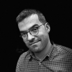
Andrea Firrincieli

Andrea Firrincieli
R&D Engineer for Sustainable Electronics
imec

Andrea Firrincieli

Abstract
Semiconductor technology is essential for enabling a sustainable future, but it also poses significant environmental challenges, such as high emissions, water use, resource depletion, and e-waste. Imec's Sustainable Semiconductor Technologies and Systems (SSTS) program aims to address these challenges by reducing the environmental impact of fab processes.In this presentation, in addition to discussing the general trends of emissions related to the manufacturing of advanced IC technologies, the contribution of the upstream emissions related to manufacturing of wet chemicals will be highlighted. The findings are stressing the need of collaboration across the semiconductor manufacturing value chain to have a meaningful impact on the total emissions embedded in integrated circuits.

Biography
Lars-Åke Ragnarsson received the M.S. and Ph.D. degrees in electrical engineering from Chalmers University of Technology, Göteborg, Sweden, in 1993 and 1999, respectively. Between 2000 and 2002, he did postdoctoral studies with the IBM T.J. Watson Research Center, Yorktown Heights, NY, focusing mainly on electrical characterization of high-k dielectrics. Since 2002, he has been with the Interuniversity Microelectronics Center (imec), Leuven, Belgium. From 2002 to 2021 he worked mainly on the development of advanced technologies using high-κ dielectrics and metal gates. As of 2021, Lars-Åke is the Director of the Sustainable Semiconductor Technologies and Systems Program which focus on the sustainability of current and future compute and memory technologies.

10:25
Reduction of Process Chemicals and Energy Use in Single-Wafer Process Applications
  Jim Snow, Sr. Technologist, SCREEN SPE
Reduction of Process Chemicals and Energy Use in Single-Wafer Process Applications
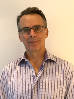
Jim Snow

Jim Snow
Sr. Technologist
SCREEN SPE

Jim Snow

Abstract
Sustainability is important for modern semiconductor manufacturing facilities to reduce environmental impact, ensure regulatory compliance, enhance corporate social responsibility, and lower operating costs. Semiconductor wafer fabs consume a significant amount of water, chemicals and energy and generate a large amount of waste, which can have a significant environmental impact. For example, modern facilities can use up to 20 million liters of water/day. On the chemical side, sulfuric acid (H2SO4) is one of the most widely used chemicals in the microelectronics industry and the amount is expected to increase ~50% by 2021. Since wet cleaning processes account for more than one-fourth of all processes, reduction of these process chemistries presents an opportunity for engineered solutions to improve the efficiency of UPW and chemical use.SCREEN Semiconductor Solutions has recently developed and installed in high-volume manufacturing (HVM) technology for the recycling of hot UPW for single-wafer cleans that reduces UPW and energy use by 80%. Furthermore, to help reduce the environmental impact of sulfuric acid, SCREEN has developed a SPM reclaim function on their single-wafer platform that can reduce SPM use by 70% with similar process performance compared to single-pass use. By implementing sustainable practices, such as reducing chemical and UPW consumption and improving energy efficiency, semiconductor facilities can reduce their environmental impact and contribute to a more sustainable future.

Biography
Dr. Jim Snow is a Senior Technologist in the Global Sustainability group at SCREEN Semiconductor Solutions. He has over 30 years in the semiconductor industry on both the liquid and gas sides of the business. He began his semiconductor career developing specialty gas purifiers and contaminant analyzers with a major component supplier, then subsequently learned the liquid side developing wet etch and clean processes at IMEC in the Ultra Clean Processing group. He received his Ph.D. in chemistry from MIT. Dr. Snow has numerous publications in journals, book chapters, patents and conference presentations. He is a member of the IRDS UPW and ESH/S groups, SEMI SCC working groups and co-lead of the SIA PFAS Consortium Articles WG.

10:40
Fluid Simulation Over A Rotating Disk: Momentum And Mass Transfer Across The Wafer Boundary
  Naser Belmiloud, R&D Engineer, SCREEN SPE
Fluid Simulation Over A Rotating Disk: Momentum And Mass Transfer Across The Wafer Boundary
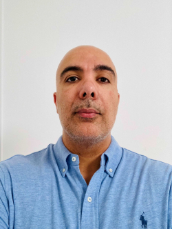
Naser Belmiloud

Naser Belmiloud
R&D Engineer
SCREEN SPE

Naser Belmiloud

Abstract
Computational fluid dynamics (CFD) is used to optimize cleaning efficiency by adjusting fluid properties and process parameters. The research examines thickness variations across the wafer, characterizes the wavy air-liquid interface, and measures liquid velocity and viscous sublayer thickness. The results underscore the importance of turbulent structures, the balance between Coriolis and viscous forces, and the effective use of CFD LES (Large Eddy Simulation) to visualize the viscous sublayer and eddy flow.

Biography
Dr. Belmiloud earned his Master in physics and Ph.D. in Electronics from the University of Bordeaux, where he focused on MEMS-based sensors for probing fluid properties and biosensor applications. Following this, he undertook a postdoctoral fellowship in biophysics at Massey University in New Zealand. He then joined Imec and subsequently began his career at SCREEN in 2012. At SCREEN, Dr. Belmiloud held various roles, which included supporting the process, integrating new products, and overseeing R&D collaborations for SCREEN SPE in Europe.

10:55
SU-3400 Single Wafer Processor - The Evolution of the World´s No.1 Cleaning Equipment
  Mark Goeke, Sr. Manager, SCREEN SPE
SU-3400 Single Wafer Processor - The Evolution of the World´s No.1 Cleaning Equipment
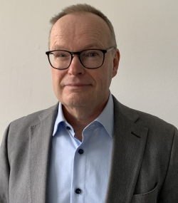
Mark Goeke

Mark Goeke
Sr. Manager
SCREEN SPE

Mark Goeke

Abstract
SCREEN Semiconductor Solutions has been developing single-wafer cleaning equipment since 1983. Since then, the company has evolved the technology by pursuing optimal treatment of the air-liquid interface on wafer surfaces. The SU-3400 inherits the stable cleaning performance of the industry-leading "SU Series" and is at the forefront of productivity and processing performance.This new flagship single-wafer processor tool features high throughput by utilizing 24 spin units at small footprint, reduction of environmental load and stable operation by using Big Data.

Biography
Mark Goeke received his Master of Science in Photo Engineering from the University of Applied Science, Cologne in 1994.After holding various positions in lithography engineering he started working with Dainippon Screen Mfg.Co (now Screen SPE, Germany) in 1999.Here he moved to hold the position of the Manager of Technical Sales & Product Engineering, responsible for technology and product engineering for Screen´s line-up of semiconductor production equipment, comprising lithography tools, single wafer processors, annealing, measurement and inspection systems.

11:10
SmartSiCTM, a Greener, Faster and Better Technology for SiC
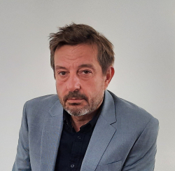
  Olivier Bonnin, General Manager, Soitec
SmartSiCTM, a Greener, Faster and Better Technology for SiC
Olivier Bonnin

Olivier Bonnin
General Manager
Soitec

Olivier Bonnin

Abstract
For 30 years, Soitec has been designing and manufacturing semiconductor-engineered substrates. Soitec is addressing markets for three key megatrends such as 5G/6G, Electrical Vehicles (EVs), and Artificial Intelligence. We foresee EVs to become a significant new growth driver using Silicon Carbide (SiC) in their power electronics systems. SiC brings several advantages over Silicon when it comes to power electronic devices. These include a higher breakdown voltage, higher operating temperature, and higher thermal efficiency.Smart-CutTM applied to SiC, generating SmartSiC TM engineered substrate aims to accelerate SiC adoption and brings the best of SiC by combining high conductivity ultra-flat pSiC and high-quality layer of mSiC for the device. This unique vertical structure allows an additional boost in the electrical performance and efficiency of power devices. On the sustainability front, SmartSiCTM, is a greener route to volume by targeting CO2 footprint equivalent to silicon wafers, mostly to vast reuse of mSIC donor wafers, obtained at a very high thermal budget.SmartSiC TM defectivity performances must be aligned on the Silicon maturity level, using the same cleaning process, equipment and reaching the same defectivity level. If there is no dedicated manufacturing line, SiC and Si wafers have to be processed together.SmartSiCTM-engineered substrate is a revolution that Soitec is not doing alone. We are collaborating with strategic partners on all fronts, from research and technology organizations to materials and equipment suppliers and leading device manufacturers.

Biography
Olivier Bonnin has been recently appointed Senior Director of Soitec's Expertise Lab, which is gathering experts in various fields, Fundamental of Physics and Simulation, Material, Process and Device.He joined Soitec in 2006 as a Product Engineering Manager and participated in the introduction of most of the existing Soitec products. For several years, he led, as General Manager, the Soitec's Wide Band Gap Business Unit resulting in the SmartSiCTM product introduction.Olivier Bonnin has authored or co-authored more than 30 papers. He has a PhD in Material sciences from CNRS.

11:30
Laser Annealing for New Generation of SiC Power Devices
  Paolo Badala', Sr. Technologist, ST Microelectronics
Laser Annealing for New Generation of SiC Power Devices
Paolo Badala'

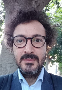
Paolo Badala'
Sr. Technologist
ST Microelectronics

Paolo Badala'

Abstract
ST has been strongly committed to sustainability for more than 25 years, through the creation of technology and solutions that enable customers to improve energy efficiency, make driving greener and increase the use of renewable energy. In the last decade, silicon carbide (SiC) has attracted increasing attention and started to play a significant role in the green economy transition, thanks to its excellent physical properties, that allow to obtain higher breakdown voltage, higher switching frequency, lower resistance, and smaller devices. Laser annealing is nowadays considered an enabling process for the new generation of SiC power device manufacturing because it allows obtaining state-of-the-art back side ohmic contacts on very thin wafers. Moreover, promising results have been obtained by using laser annealing for dopant activation and front-side ohmic contact formation.

Biography
Paolo Badalà received the M.Sc. Degree in Physics from the University of Catania (Italy) in 2004. He joined STMicroelectronics in 2007. His current research interests include the development of thin film deposition and laser annealing processes, mainly for wide bandgap semiconductors technology. He is co-author of several patents and papers published in international journals and conference proceedings.

11:50
Solid-phase epitaxial regrowth of Si:P by nanosecond laser annealing for 3D sequential integration
  Sebastien Kardiles, Sr. Manager, Leti
Solid-phase epitaxial regrowth of Si:P by nanosecond laser annealing for 3D sequential integration
Sebastien Kardiles

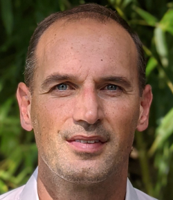
Sebastien Kardiles
Sr. Manager
Leti

Sebastien Kardiles

Abstract
In view of 3D sequential integration, an architecture with at least two levels of active devices on top of each other, there are severe thermal budget limitations for the processing of the upper level(s). To avoid any degradation of the already processed bottom level(s), ‘cold’ process modules have to be developed for the upper transistors fabrication. Two important challenges are the gate stack formation and the activation of the dopants in the source and drains. These steps usually require high-temperature processes that are no longer compatible with a 3D sequential integration. For the dopants activation in S/D regions, even Solid-Phase Epitaxial Regrowth (SPER) in classical reactors is not longer an option if the maximum acceptable temperature is limited to 400°C. UV nanosecond laser annealing (UV-NLA) is a smart alternative technique to overcome such limitations. In the present work, we will demonstrate the nanometer-by-nanometer recrystallization of amorphized silicon, using an original multi-pulse approach. We will also show that efficient active dopant activation is obtained.

Biography
Dr. Sébastien Kerdilès received a Ph.D. degree in materials science from the University of Caen, France, in 2000. Then, he worked for 2 years for a start-up in the Paris area. From 2002 to 2013, he worked for SOITEC as a research staff member first, then as a technology development manager, and finally as an SOI designer. During this period, he contributed to the industrialization of 200 & and 300mm SOI substrates manufacturing, including RF-SOI and Fully depleted SOI. In 2013, he joined CEA-LETI, where he is in charge of thermal treatments. His research interests include the investigation of pulsed laser annealing for various applications such as 3D integration, memories, and MEMS. He authored or co-authored more than 50 journal articles and conference papers and holds over 20 patents.

12:10
SCREEN Laser Annealing Technology for the Next Generation of Semiconductor
  Louis Thuries, Product Manager, SCREEN SPE
SCREEN Laser Annealing Technology for the Next Generation of Semiconductor
Louis Thuries

Louis Thuries
Product Manager
SCREEN SPE

Louis Thuries

Abstract
Ultimate control of thermal budget, both in time and in depth, is made possible by combining surface-selective anneal enabled by UV laser and control of heat diffusion enabled by tuning the irradiation duration in the µs timescale.Such technology opens a new space in between sub-melting standard techniques, such as furnace anneal or flash lamps anneal, and nanosecond melting UV laser anneal.The emergence of these laser annealing products will open the door to advanced process integration paths for next generation of semiconductor devices.For Si IGBT, UV µs LA allows activation of p/n junction in a diffusion-less single step process. Thanks to ultimate control of heat penetration depth, UV µs LA is suitable for all kind of profiles up to 5 µm while staying compatible with thin wafers.SiC power devices have emerged as a breakthrough technology for a wide range of applications, from inverter for automotive to fast charging stations. Fabricating low resistance ohmic contact with good reliability and mechanical performances is still challenging, and UV µs-LA is shown to lead to uniform and continuous formation of NixSiy films. Finally, crystal curing and dopant activation after ion implantation by laser anneal, in a cost-effective and protective capping-less integration, is a major step forward and opens new routes for SiC power MOSFETs.Next generation of CMOS will have their overall performances limited by the metal interconnects “BEOL”. Indeed, diminution of the width of these interconnects leads to an important increasing of the line resistivity. Enlargement of the grain size can prevent the electron scattering at the grain boundaries and boost metal lines performance. UV µs-LA has already demonstrated impressive grain size enlargement on copper and ruthenium while remaining compatible with buried structures.

Biography
Louis Thuries is the product manager at SCREEN LASSE.Prior to that, he was based in Taiwan as an application, process, and product development engineer. He extensively worked with R&D centers (LETI/imec/IBM) for application development, focusing on advanced logic, CIS, power, and memory devices.Before LASSE, he was working on GaN HEMT development in Grenoble.