Thursday, November 16, 2023
 

SOI Industry Consortium

15:10 Welcome from SOIIC, Patrick Martin, Soitec & Chair, SOI Industry Consortium
15:20 Reserved to Stellantis
15:40
SOI for HV and Power Management Applications
  Piet Wessels, Fellow and senior director HV technologies, nxp semiconductors
SOI for HV and Power Management Applications
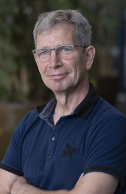
Piet Wessels

Piet Wessels
Fellow and senior director HV technologies
nxp semiconductors

Abstract
NXP is using SOI substrates for BCD technologies. The SOI helps the products to be robust in the automotive environment. Since it allows transistors and other componenets to be fully isolated with oxide. Over the years NXP has build a broad platform of products for the automotive domain, using SOI.

Biography
Piet Wessels studies Physics at the Delft Unverisity of technology.He started at Philips semiconductors in 1987. He worked on bipolar, cmos and Bicmos technologies. Since 2006 he leads various team in the area of BCD technology and SiGe based technologies. In 2015 the span of control has been further increased after the merger with freescale semicobductors.

16:00
FD-SOI Technology scaling down to 10nm.
  Olivier Faynot, Executive VP and GM of Silicon Division, CEA-Leti
FD-SOI Technology scaling down to 10nm.
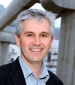
Olivier Faynot

Olivier Faynot
Executive VP and GM of Silicon Division
CEA-Leti

Olivier Faynot

Abstract
FD-SOI technologies are now available at 28nm and 22nm, with outstanding RF and low Power Performances, suitable for connectivity, mobile and automotive applications. Technological nodes below 22nm have to be developped to enable better performance and competitivity.In this talk, we will detail the on-going work towards a 10nm node definition.

Biography
Olivier Faynot received the M.Sc and Ph.D. degrees from the Institut National Polytechnique de Grenoble, France in 1991 and 1995, respectively. His doctoral research was related to the characterization and modeling of deep submicron Fully Depleted SOI devices fabricated on ultrathin SIMOX wafers.He joined LETI (CEA-Grenoble, France) in 1995, working on Partially Depleted and Fully Depleted SOI technologies development in the frame of Industrial Partnerships.From 2008 to 2017, he managed various teams focussed on advanced CMOS, memories and 3D technology integration and was assigned on manufacturing sites to implement FDSOI technologies.During that period, he was engaged in the transfer to production of 28nm and 22nm FDSOI technologies with industrial partners. Those technologies are now available in production.From 2017 to 2019, he managed the Patterning department at CEA-LETI, within the Silicon Technology division.Since 2019, he is managing the whole Silicon Component division at CEA-LETI.He is author and co-author of more than 300 scientific publications in journals and international conferences, and was successively in the committees of the main international Semiconductors conferences like International Electron Device Meeting (IEDM), the symposium on VLSI Technology, the IEEE International SOI conference, the EUROSOI network, the Solid State Device and Materials (SSDM) conference and the International S3S conference.He received the ‘Général Férié’ award in 2012 and the ‘Electron d’Or’ award with CEA-Leti, ST Microelectronics and SOITEC in 2017.

16:20 Panel discussion

SOI: Developing Applications with Improved Performance

Moderation Junko Yoshida, Editor in Chief, The Ojo-Yoshida Report, The Ojo-Yoshida Report
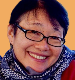
Junko Yoshida

Junko Yoshida
Editor in Chief, The Ojo-Yoshida Report
The Ojo-Yoshida Report

Junko Yoshida

Biography
Junko Yoshida is the editor in chief of The Ojo-Yoshida Report, covering the business and technology of semiconductors. Junko has always been a “roving reporter” in the most literal sense. She pursued a peripatetic journalism career, breaking stories, securing exclusives, and filing incisive analyses from Tokyo, Silicon Valley, Paris, New York, and China.Junko writes and speaks authoritatively on consumer electronics, automotive, semiconductors, emerging technologies, technology’s impact on people & society and intellectual property, with a deep understanding of the business strategies that companies are pursuing to compete on a global scale. ‌‌During her three decades at EE Times, Junko rose up the ranks from Tokyo correspondent to West Coast bureau chief, European bureau chief, news editor, and editor-in-chief. She earned a reputation as an innovator, shepherding EE Times’ expansion into e-books, including the award-winning “The Day the Lights Went out in Japan”; the EE Times on Air podcast; conferences, such as the EE Times Roadmap to Next-gen EV & AV; and The Artful Engineer video podcast, which explores the intersection of art and engineering.‌

Panelists
  • Aniket Agshikar, Director, Global Quality Engineering, GlobalFoundries
  • Aniket Agshikar

    Aniket Agshikar
    Director, Global Quality Engineering
    GlobalFoundries

    Aniket Agshikar

    Biography
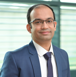
    Aniket Agshikar Director, Global Quality Engineering @ GlobalFoundriesDresden, Germany With a robust career spanning 15 years at GlobalFoundries (GF), Aniket has cultivated a rich tapestry of experience across various functional teams. Beginning in test engineering, His journey has encompassed roles in R&D, Process Integration, and pivotal contribution to multiple 28nm customer projects. Furthermore, as the 22FDX platform owner, he demonstrated expertise in leading-edge technology development, customer engagement and production ramp. From November 2021, he took the helm at Fab1 Quality, showcasing a commitment to excellence. Most recently, this dedication has been further exemplified in a transition to a Global Quality Engineering role, ensuring that GlobalFoundries continues to be at the forefront of semiconductor excellence.He has completed Executive MBA from ESMT, Berlin and Master's degree in Electrical Engineering from NUS, Singapore. His key interests are problem solving & decision analysis, technology development, strategy, program management and team/people development. He loves to solve complex challenges and continues to build a Total Quality Culture at GF. He is married with one son and enjoys watching movies, listening to Bollywood music, cooking and traveling.

  • Jani Karttunen, Product Manager, Okmetic Oy
  • Jani Karttunen

    Jani Karttunen
    Product Manager
    Okmetic Oy

    Jani Karttunen

    Biography
    Mr. Jani Karttunen is Product Manager of the Patterned Wafer Products at Okmetic, the leading supplier of advanced silicon wafers. He has been with Okmetic since 2007, in various positions including sales, new business development and technical customer support. He has 20 years of hands-on experience in process development and process integration of state-of-the-art MEMS devices. His career to date includes engineering positions at VTI Technologies Oy (now Murata Finland), the State Research Centre of Finland (VTT) and petrol company Neste Oyj. Mr. Karttunen received his Master’s degree in Materials Science at the Helsinki University of Technology (now Aalto University) Finland.

  • Erwan Hemon, Vice President of Technology and Innovation, NXP
  • Erwan Hemon
    Vice President of Technology and Innovation
    NXP

    Erwan Hemon

    Biography
    Erwan HEMON is Vice President of Technology and Innovation in NXP semiconductors working in Business Line Advanced Analog responsible for Technology & Innovation as well as ESD-EMC Center of excellence and Back End activities. He has been in this role since 2016 based in Toulouse (France).In addition , Erwan HEMON is the CTO and General Manager of Energy and Lighting Business Line for Datang NXP Semiconductors, responsible for BMS (Battery Monitoring Systems) product development.Prior this he worked 10 years for Freescale as R&D Director for Analog division (based in Phoenix and Toulouse) , and 10 years for Motorola Semiconductors as design manager where he managed the Toulouse design centers (France), focused on mixed signal design in smart-power technology for use in automotive and Power Over Ethernet applications.Over those years he worked on products for applications like BMS (Battery Monitoring Systems), Airbags, Braking systems (ABS, ESP), Automotive networking transceivers, Motor driver (H-bridge, 3Ph motor drivers) , DFI (Direct Fuel Injection), Engine Management , Power Management, E-switch (electronic switches) and is familiar with most automotive related processes like AECQ100, ISO2626 (functional safety) , ESD and EMC .Before joining Motorola Semiconductors, he worked as a design engineer at Philips Semiconductors in Caen (France) on various analog products for Hard Disk Drive market as well as telephony ICs.Overall he has been working on Mixed Signal IC development for 30 years and hold more than 10 patents granted in those area.Erwan Hemon graduated as an electronic engineer from the French Grande Ecole “ENSERG” Grenoble’s National Institute of Electronics and Radio-Electricity in 1990.

  • Nicolas Grossier, Product Line Manager - Senior Principal Engineer, STMicroelectronics
  • Nicolas Grossier

    Nicolas Grossier
    Product Line Manager - Senior Principal Engineer
    STMicroelectronics

    Nicolas Grossier

    Biography
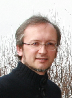
    Nicolas Grossier is Automotive 32-bit MCU Manager at STMicroelectronics, in charge of the design development of the stellar G product family. After initial experience in developing CPU and multicore (MCU+DSP) solutions, Nicolas worked on a wide range of automotive products spreading from airbags, braking, and power train to body controllers. Today, with his eclectic knowledge in low-power, embedded memory, safety, and security, he is guiding automotive engineers develop more efficient applications and powerful integrated ECUs using STMicroelectronics Stellar MCUs for software-defined vehicles.

17:20 Closing Remarks, Patrick Martin, Soitec & Chair, SOI Industry Consortium