Thursday, November 16, 2023
 

SOI Industry Consortium

15:10 Welcome from SOIIC, Patrick Martin, Soitec & Chair, SOI Industry Consortium
15:20 Reserved to Stellantis
15:40 SOI for High-Voltage Power Mgmt. Applications, Piet Wessels, NXP Fellow and Senior Director of HV and RF Technologies Consortium
16:00
FD-SOI Technology scaling down to 10nm.
  Olivier Faynot, Executive VP and GM of Silicon Division, CEA-Leti
FD-SOI Technology scaling down to 10nm.
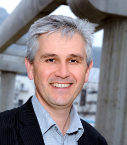
Olivier Faynot

Olivier Faynot
Executive VP and GM of Silicon Division
CEA-Leti

Olivier Faynot

Abstract
FD-SOI technologies are now available at 28nm and 22nm, with outstanding RF and low Power Performances, suitable for connectivity, mobile and automotive applications. Technological nodes below 22nm have to be developped to enable better performance and competitivity.In this talk, we will detail the on-going work towards a 10nm node definition.

Biography
Olivier Faynot received the M.Sc and Ph.D. degrees from the Institut National Polytechnique de Grenoble, France in 1991 and 1995, respectively. His doctoral research was related to the characterization and modeling of deep submicron Fully Depleted SOI devices fabricated on ultrathin SIMOX wafers.He joined LETI (CEA-Grenoble, France) in 1995, working on Partially Depleted and Fully Depleted SOI technologies development in the frame of Industrial Partnerships.From 2008 to 2017, he managed various teams focussed on advanced CMOS, memories and 3D technology integration and was assigned on manufacturing sites to implement FDSOI technologies.During that period, he was engaged in the transfer to production of 28nm and 22nm FDSOI technologies with industrial partners. Those technologies are now available in production.From 2017 to 2019, he managed the Patterning department at CEA-LETI, within the Silicon Technology division.Since 2019, he is managing the whole Silicon Component division at CEA-LETI.He is author and co-author of more than 300 scientific publications in journals and international conferences, and was successively in the committees of the main international Semiconductors conferences like International Electron Device Meeting (IEDM), the symposium on VLSI Technology, the IEEE International SOI conference, the EUROSOI network, the Solid State Device and Materials (SSDM) conference and the International S3S conference.He received the ‘Général Férié’ award in 2012 and the ‘Electron d’Or’ award with CEA-Leti, ST Microelectronics and SOITEC in 2017.

16:20 Panel discussion

Topic Coming Soon

Panelists
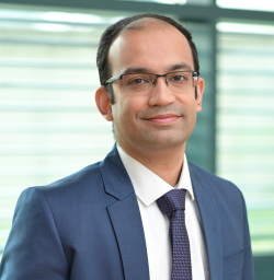
  • Aniket Agshikar, Director, Global Quality Engineering, GlobalFoundries
  • Aniket Agshikar

    Aniket Agshikar
    Director, Global Quality Engineering
    GlobalFoundries

    Aniket Agshikar

    Biography
    Aniket Agshikar Director, Global Quality Engineering @ GlobalFoundriesDresden, Germany With a robust career spanning 15 years at GlobalFoundries (GF), Aniket has cultivated a rich tapestry of experience across various functional teams. Beginning in test engineering, His journey has encompassed roles in R&D, Process Integration, and pivotal contribution to multiple 28nm customer projects. Furthermore, as the 22FDX platform owner, he demonstrated expertise in leading-edge technology development, customer engagement and production ramp. From November 2021, he took the helm at Fab1 Quality, showcasing a commitment to excellence. Most recently, this dedication has been further exemplified in a transition to a Global Quality Engineering role, ensuring that GlobalFoundries continues to be at the forefront of semiconductor excellence.He has completed Executive MBA from ESMT, Berlin and Master's degree in Electrical Engineering from NUS, Singapore. His key interests are problem solving & decision analysis, technology development, strategy, program management and team/people development. He loves to solve complex challenges and continues to build a Total Quality Culture at GF. He is married with one son and enjoys watching movies, listening to Bollywood music, cooking and traveling.

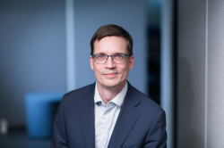
  • Jani Karttunen, Product Manager, Okmetic Oy
  • Jani Karttunen

    Jani Karttunen
    Product Manager
    Okmetic Oy

    Jani Karttunen

    Biography
    Mr. Jani Karttunen is Product Manager of the Patterned Wafer Products at Okmetic, the leading supplier of advanced silicon wafers. He has been with Okmetic since 2007, in various positions including sales, new business development and technical customer support. He has 20 years of hands-on experience in process development and process integration of state-of-the-art MEMS devices. His career to date includes engineering positions at VTI Technologies Oy (now Murata Finland), the State Research Centre of Finland (VTT) and petrol company Neste Oyj. Mr. Karttunen received his Master’s degree in Materials Science at the Helsinki University of Technology (now Aalto University) Finland.

17:20 Closing Remarks, Patrick Martin, Soitec & Chair, SOI Industry Consortium