Wednesday, November 15, 2023
 

Session 1: Mega Trends and Opportunities for Advanced Packaging and Front-End Integration

09:00
Welcome Remarks
  Laith Altimime, President, SEMI Europe
Welcome Remarks
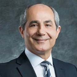
Laith Altimime

Laith Altimime
President
SEMI Europe

Laith Altimime

Abstract
Coming Soon

Biography
Laith Altimime, as President of SEMI Europe, leads SEMI’s activities in Europe and the Middle East and Africa (EMEA). Altimime has P&L responsibility as well as ownership of all Europe region programs and events, including SEMICON Europa. He is responsible for establishing industry standards, advocacy, community development, expositions, and programs. He provides support and services to SEMI members worldwide that have supply chain interests in Europe. He manages and nurtures relationships with SEMI members in the region and globally as well as with local associations and constituents in industry, government, and academia. Altimime has more than 30 years of international experience in the semiconductor industry. Prior to joining SEMI in 2015, He held senior leadership positions at NEC, KLA-Tencor, Infineon, Qimonda and imec. Altimime holds an MSc from Heriot-Watt University, Scotland.

09:10
Lights Outside Tunnel
  Douglas Yu, Vice President of TSMC R&D and TSMC Distinguished Fellow, TSMC
Lights Outside Tunnel
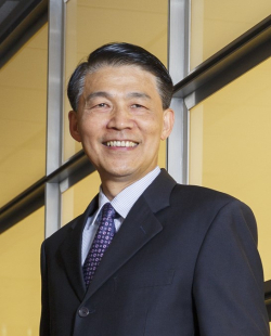
Douglas Yu

Douglas Yu
Vice President of TSMC R&D and TSMC Distinguished Fellow
TSMC

Douglas Yu

Abstract
High Performance Compute (HPC) and AI/ML have been realized by advanced nodes IC and advanced system integration technologies. Device /chip scaling and heterogeneous system integration, eg. TSMC 3DFabricTM, which consists of CoWoS®, InFO and SoIC®, become the twin engine to drive semiconductor technology. Recent new wave of generative AI with LLM showed that HPC and AI/ML have tremendous room for future growth. In the meantime, higher performance compute with higher energy efficiency become even more critical requirements than ever to support the demand. We will continue the scaling of both device/IC and advanced system in classical m-electronics based computing system. Furthermore, photonics-based system integration technology will be added which are complementary to the classical system integration to meet the ever-increasing energy efficient performance requirements for future HPC and AI/ML.

Biography
DDoug Yu is a Vice President of TSMC R&D and TSMC Distinguished Fellow, responsible for system integration technology pathfinding. Previously, Doug has pioneered and led TSMC Cu/Low-K technology development, industry first wafer-level system integration technology platform, TSMC 3DFabricTM, including CoWoS®, InFO and SoICTM, and TSMC COUPE, a photonics-based system integration technology.Prior to TSMC, Doug worked with AT&T Bell Labs. He received Ph.D. degree in Materials Science and Engineering from Georgia Institute of Technology, Atlanta, GA.Doug is a recipient of IEEE Rao Tummala Award, IEEE EPS Microelectronics Manufacturing Award, and President Science Prize, Taiwan. He is an IEEE Fellow, TSMC Distinguished Fellow, and a member of National Academy of Engineering. He has given numerous invited/keynote/plenary speeches in international conferences and published 150+ papers to elevate system integration technology profile. He has (co)-authored 1500+ US granted semiconductor technology patents.

09:30
Bridging Front End, Packaging and Substrates to Advance the Semiconductor Roadmap
  Oreste Donzella, Executive VP, KLA
Bridging Front End, Packaging and Substrates to Advance the Semiconductor Roadmap

Oreste Donzella
Executive VP
KLA

Oreste Donzella

Abstract
For over 50 years, Moore’s Law has defined the pace of the semiconductor industry with its ability to scale transistor density every 2 years. While the frontend roadmap is still progressing thanks to EUV lithography and other process technology innovations, it’s no longer sufficient to keep pace with the diversified demand of the new digital society.In recent years, we have seen an acceleration of technical innovations in IC packaging and IC substrates to complement front end wafer fabrication technologies and meet performance, power, and cost requirements.The implementation of heterogeneous integration started long ago with the first multi-chip modules and 2D packages and is now accelerating with several new 2.5 and 3D architectures serving various end-applications, including high-performance computing, mobile, and networking, among others.With interconnect geometry scaling, we see the need and the opportunity to bridge process equipment and process control methodologies across the three worlds of front-end, packaging and substrates. These once completely separated domains are becoming integrated just like the packages and systems they create.The adoption of front end-like technologies and methodologies into packaging and IC substrates is not trivial and it requires innovation and customization to meet cost and performance requirements.KLA is partnering with key industry players to bridge these three worlds and this presentation will show the challenges we are facing and problems we are solving to advance the semiconductor technology roadmap.

Biography
Oreste Donzella serves as Executive Vice President of Electronics, Packaging and Components.In his 20 years at KLA, he has held leadership roles in the field of customer engagement, process control solutions, application development, strategic marketing and product development. Before joining KLA, Mr. Donzella worked at Texas Instruments and Micron, where he held various engineering and management positions in process integration and yield enhancement.Mr. Donzella currently serves as a member of the SEMI North American Advisory Board.Mr. Donzella earned his bachelor’s degree and master’s degree in electrical engineering from the Sapienza University of Rome.

09:50 Opening Remarks by Session Chair
  Roland Rettenmeier, Senior Product Marketing Manager, Evatec
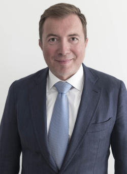
Roland Rettenmeier

Roland Rettenmeier
Senior Product Marketing Manager
Evatec

Biography
Roland Rettenmeier qualified as a Mechanical Engineer in 1997 and completed his MBA studies at Vienna, Austria in 2005. Roland extended his education through other international courses and programs since that time (e.g. Six Sigma Program with AT&S and Nokia; Innovation Technology Leader at Stanford University).Roland has worked in the field of Electronics and Semiconductor manufacturing since 2001, managing multiple international projects. After joining Evatec in 2016 as Senior Product Marketing Manager (PMM) within the Business Unit for Advanced Packaging, he focused on business development for Panel Level Packaging where Evatec has now become the recognised market leader for thin film technology solutions. Since 2020 he has also supported development of Evatec’s wafer level packaging solutions business.In addition to his market and customer responsibilities, Roland represents Evatec in the Panel Level Packaging consortium of Fraunhofer IZM Berlin, in the Packaging Research Center at Georgia Tech, USA and in the Panel Level Packaging Consortium at the NCAP in Wuxi, China.

09:55
Latest Solutions in the Energy Efficiency of Electronic Systems
  Hannes Voraberger, Corporate Vice President R&D, AT&S Austria Technologie & Systemtechnik Aktiengesellschaft
Latest Solutions in the Energy Efficiency of Electronic Systems
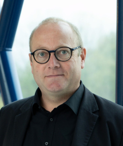
Hannes Voraberger

Hannes Voraberger
Corporate Vice President R&D
AT&S Austria Technologie & Systemtechnik Aktiengesellschaft

Hannes Voraberger

Abstract
Digitalization without further improvement in the energy efficiency of electronic systems will lead to a dramatic increase in energy requirements for data processing. The solution is based on processing systems with smaller nodes and a highly efficient power supply. Interconnect technology based on advanced IC substrate technologies offer great opportunities for improved signal processing and efficient power supply. Latest solutions will be presented in this talk.

Biography
Dr. Voraberger assumed his current position in 2010, as head of AT&S corporate research and development department. Previously Dr. Voraberger was responsible for AT&S corporate intellectual property and governmental funding.He also established the R&D center in AT&S Shanghai (China) and was project leader for AT&S research and development in AT&S Leoben (Austria).Dr. Voraberger studied industrial chemistry at Graz University of Technology, awarded multiple patents and has published several papers.

10:15 Coffee break
10:55
Advanced Packaging Materials and Open Innovation at Resonac
  Hidenori Abe, Senior Director, Head of R&D center Electronics business, Resonac
Advanced Packaging Materials and Open Innovation at Resonac
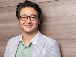
Hidenori Abe

Hidenori Abe
Senior Director, Head of R&D center Electronics business
Resonac

Hidenori Abe

Abstract
On January 1, 2023, Showa Denko K.K. and Showa Denko Materials Co., Ltd. merged and transformed themselves into newly integrated company "Resonac".Accommodating post-5G/6G systems will require an increased density of IC chips and other components to increase processing speed highly. Therefore, there is a need for technologies that allow for high -density packaging of differing chips within a single semiconductor package. Resonac has started Packaging Solution Center as new R&D center to propose one-stop solution for customers in 2019 and established the co-creative packaging evaluation platform “JOINT2” with leading companies to accelerate the development of advanced materials, equipment and substrates for 2.xD and 3D package in October, 2021.We are developing fine vertical/lateral interconnect technology and the study of fabrication and reliability for the extremely large 2.5D advanced package.The presentation will cover the significance and strengths of JOINT2, and updates on research and development. “Resonac is open to collaborations including 1on1 co-development with any partners and is currently investigating in JOINT programs outside Japan. This shall significantly benefit customers, partners as well as equipment makers in the future ecosystem”

Biography
Mr. Abe is leading R&D of semiconductor materials in general and promoting co-creation activities at Resonac, after serving as a general manager of CMP slurry business sector and a corporate marketing manager at Hitachi Chemical.He was involved in the launch of the Packaging Solution Center, which is open innovation hub in advanced packaging development.He joined Hitachi chemical in 1998 and was involved in the development of semiconductor molding compounds.He holds an Executive MBA from Oxford, UK.

11:15
A European 3D Heterogeneous Integration Pilot Line – a Leap ahead to Achieve Technology Leadership
  Michael Töpper, Senior Expert Heterointegration Research Fab Microelectronics Germany (FMD), Fraunhofer FMD
A European 3D Heterogeneous Integration Pilot Line – a Leap ahead to Achieve Technology Leadership

Michael Töpper
Senior Expert Heterointegration Research Fab Microelectronics Germany (FMD)
Fraunhofer FMD

Abstract
The digital transformation of society and economy creates an increasing demand to transfer, process and store vast amounts of data generated in the context of technologies such as artificial intelligence (AI) and the Internet of Things (IoT). Therefore, future electronic systems like autonomous systems using high-performance computing (HPC) and edge computing systems, sensor-integrated systems and bio-integrated devices will require more and more functions that cannot be managed by a single chip, even if advanced system on chip (SoC) concepts are used. Therefore, advanced 3D heterogeneous integrated systems are the next step of evolution of the IC scaling. To support this a roadmap for required technology developments in heterogeneous integration has been defined by a joint working group of FMD and industry partners with a horizon of 2030 and beyond.It includes lithographical scaling that supports sub µm hybrid bonds pitches. The thermal management of extreme heat dissipation and topological limitations by STCO measures, new materials and new cooling methods. Comprehensive testing of dies to achieve an economically reasonable yield in a complex heterogeneous integration process containing a higher number of dies. To improve the processes and to understand failure mechanisms an appropriate failure analysis has to be codeveloped together to address fails in 3D stacks. Without the possibility to manufacture parts throughout a complete assembly process the full assessment of the impact of these topics is not possible. By looping in wafer or dies of leading-edge CMOS or special technologies like GaN from industry partners or collaborating research and technology organizations advanced processor devices can be realized through an innovative pilot line. Such a pilot line also allows to explore an automotive grade technology along with other industrial applications requiring high robustness. Together with the planned investments into Silicon frontend manufacturing and assembly in Europe as announced e.g. by Intel the heterogeneous integration pilot line at the chip, package and organic substrate level plays a key role to excel the position of Europe as hub for assembly and test.The paper will be presented together with Intel and Siemens EDA.

Biography
Michael Töpper studied chemistry at the University of Karlsruhe and received his doctorate in materials science from the Technical University of Berlin. He has been working in the field of assembly and connection technology for microelectronics since 1994, initially at the TU Berlin, then as a group leader at Fraunhofer IZM including a year at the University of Utah as an assistant professor and until 2021 as a business developer for the entire IZM. Today he represents the Research Fab Microelectronics Germany (FMD) as an senior expert for technologies and cooperation with a focus on heterogenous integration.

11:35
Total Process Integration of Plasma Dicing for Advanced Packaging
  James Weber, Senior Business Development Manager, Panasonic Connect Europe
Total Process Integration of Plasma Dicing for Advanced Packaging
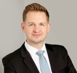
James Weber

James Weber
Senior Business Development Manager
Panasonic Connect Europe

James Weber

Abstract
Due to the impact of the COVID-19 pandemic, digital technology has become increasingly pervasive in modern society. Semiconductors are used as the power source for digital devices such as smartphones, computers, televisions, automobiles, aircraft, medical equipment, and more. Furthermore, semiconductor demand is expanding into new fields including artificial intelligence, robotics, drones, VR technology, and blockchain.In particular, there is growing demand for high-performance semiconductors such as memory, microprocessors, and AI chips and the proliferation of 5G communications has also necessitated high-speed and high-reliability semiconductors, further driving demand.In the field of advanced packaging technology, the adaptation of 2.5D and 3D stacking technology is expanding to increase the degree of packaging integration. Wafer thinning, wafer singulation and bonding technology have become more important and necessary in realizing these stacked packages.To advanced packages in high density, it is necessary to stack thinner chips and/or wafers, and it is necessary to perform bonding through pads, bumps and micro bumps, or direct bonding between flat surfaces. Therefore, in order to realize a higher density stacked package structure, it is necessary to reduce the vertical direction of bonding distance. However, conventional dicing methods such as blade and laser dicing have the issue of particle and debris creation, which make it more difficult to reduce the vertical direction of bonding distance.Plasma Dicing is a promising singulation technology that dices wafers mounted on metal ring frames by plasma processing. Furthermore, Plasma Dicing not only enables stronger chip strength, but also realizes particle-free and debris-free singulation, keeping the wafer surface and bonding surface clean.Panasonic has developed a multi-chamber Plasma Dicing system with up to 4 chambers for 12-inch wafers, as a mass production system for memory and logic circuits, which will be introduced in detail in the presentation.This system enables the processing of both of bare wafers and wafers mounted on metal ring frames, which is suitable for stacked dies and chip-on-wafer structures. The construction of this new system has been improved to achieve high density and uniformity of the plasma source. Research on the application for compound semiconductors, including the study of power devices and VCSELs is also progressing and advancing.Furthermore, there are successful examples of applying the system to GaN-on-Si, GaAs, etc, which will also be introduced in the presentation.Panasonic established the Plasma Dicing Demonstration Center in 2016 and has continuously developed advanced Plasma Dicing technology. Total process integration of Plasma Dicing has been realized.

Biography
James Weber studied engineering at the University of Adelaide in Australia. Since graduating, he has held roles in Technical Support Engineering, Project Management and Sales. Since 2016 he is the Senior Business Development Manager for Microelectronics Equipment at Panasonic Connect Europe. James’ main target is the establishment of new business opportunities in the European backend and frontend semiconductor industry in the fields of Flip-chip Bonding, Plasma Cleaning, Dry Etching and Plasma Dicing Technologies.

11:55 Key Takeways from Session Chair
  Roland Rettenmeier, Senior Product Marketing Manager, Evatec
Roland Rettenmeier

Roland Rettenmeier
Senior Product Marketing Manager
Evatec

Biography
Roland Rettenmeier qualified as a Mechanical Engineer in 1997 and completed his MBA studies at Vienna, Austria in 2005. Roland extended his education through other international courses and programs since that time (e.g. Six Sigma Program with AT&S and Nokia; Innovation Technology Leader at Stanford University).Roland has worked in the field of Electronics and Semiconductor manufacturing since 2001, managing multiple international projects. After joining Evatec in 2016 as Senior Product Marketing Manager (PMM) within the Business Unit for Advanced Packaging, he focused on business development for Panel Level Packaging where Evatec has now become the recognised market leader for thin film technology solutions. Since 2020 he has also supported development of Evatec’s wafer level packaging solutions business.In addition to his market and customer responsibilities, Roland represents Evatec in the Panel Level Packaging consortium of Fraunhofer IZM Berlin, in the Packaging Research Center at Georgia Tech, USA and in the Panel Level Packaging Consortium at the NCAP in Wuxi, China.


Session 2: Smarter Supply Chain Solutions for a Sustainable Ecosystem

12:00 Opening Remarks by Session Chair
  Ruby Yan, Director Human-Machine-Interface HMI, Globalfoundries
Ruby Yan

Ruby Yan
Director Human-Machine-Interface HMI
Globalfoundries

Biography
Ruby is a Business Line director in AIM Strategic Business Unit. She is responsible for HMI (Human-Machine-Interface) product line in wearable, AR/VR, smart home and machine vision applications.

12:05
Environmental Footprint Chip Manufacturing
  Lars-Ake Ragnarsson, Program Director Sustainable Technologies and Systems (SSTS), imec
Environmental Footprint Chip Manufacturing

Lars-Ake Ragnarsson

Lars-Ake Ragnarsson
Program Director Sustainable Technologies and Systems (SSTS)
imec

Lars-Ake Ragnarsson

Abstract
Coming Soon

Biography
Coming Soon

12:25
3D X-Ray Inspection – Game changer for Advanced Packaging
  Isabella Drolz, Vice President Product Marketing, Comet Yxlon GmbH
3D X-Ray Inspection – Game changer for Advanced Packaging
Isabella Drolz

Isabella Drolz
Vice President Product Marketing
Comet Yxlon GmbH

Isabella Drolz

Abstract
The global demand for high-end computing power driven by smartphones, IoT applications, High-performance computing, and new mobility applications is constantly rising while facing miniaturization demands. The semiconductor industry is all about identifying and solving these challenges and thereby, yield and process control is core for foundries and its importance increased even more through the introduction of advanced packaging.In today’s environment two things can be observed. One, prototyping and verification costs exponentially increase while node sizes decrease. Two, a change from typical inspection methods like optical or FIB-SEM to advanced non-destructive inspection techniques like X-ray inspection.Ultimately advanced packaging companies seek non-destructive automated inspection tools which are fast enough to provide value within their production processes, increase yield and reduce waste at an early stage. This presentation will give an overview on how X-Ray and CT inspection can provide value-added data and information for exactly that.

Biography
Isabella Drolz is the Vice President Product Marketing at Comet Yxlon, which is the industrial X-ray & CT inspection system division of Comet. Comet Yxlon provides X-ray & CT inspection solutions for R&D labs & production environments, especially for Semiconductor customers to enhance their productivity. In her role she is responsible for product management, business development, global application solution centers and marketing at Comet Yxlon. Isabella has next to her industrial engineering education, a Bachelor of Science in International Business Administration and a MBA degree from Southern Nazarene University in Oklahoma City, USA. She has held several management positions in the mechanical and plant engineering industry driving market-oriented product development.

12:45
Digitalization of Chemical Process Design for Semiconductor Materials Manufacturing
  Thorsten vom Stein, Director, Head of Process Design Semiconductor Materials, Merck
Digitalization of Chemical Process Design for Semiconductor Materials Manufacturing
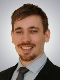
Thorsten vom Stein

Thorsten vom Stein
Director, Head of Process Design Semiconductor Materials
Merck

Thorsten vom Stein

Abstract
The drive to scale nodes towards physical limits, known as "More than Moore", and the adoption of 3D architecture in chip integration strategies for advanced logic and memory applications has led to an unprecedented demand for high-quality and dependable materials solutions. This presentation focuses on the digitalization of chemical process design for semiconductor materials manufacturing, employing molecular precision. It delves into the data-driven approaches used to streamline manufacturing processes from laboratory to HVM scale by leveraging connected asset infrastructures for cost optimization, quality, reliability, and sustainable excellence. Moreover, this talk emphasizes the importance of diversity and inclusion in fostering the "leap of faith" culture necessary for this digital revolution.

Biography
Professional ExperienceSince January 2022 Director, Head of Process Design Semiconductor MaterialsJune 2020 - January 2022 Director, Head of Process Development Semiconductor Materials EuropeJan. 2018 - May 2020 Associate Director Process Technology Japan, Chemical Lead of ProcessDevelopment Performance Materials Asia (Expatriate Assignment)Jul. 2015 – Dec. 2017Laboratory Head at Merck KGaA Process DevelopmentMarch 2014 - July 2015 Alexander-von-Humboldt Foundation research fellow (Feodor Lynen program) in the group of Professor D. W. Stephan at the University of TorontoEducationOctober 2010 – March 2014 PhD thesis (summa cum laude) “Catalytic Multistep Hydrogenation andHydrogenolysis Reactions for the Utilization of Renewable Carbon Resources”’ in the group of Professor W. Leitner as part of the cluster of excellence „Tailor Made Fuels from Biomass“ (TMFB) at the ITMC, RWTH Aachen UniversityAugust 2010 Graduation diploma (Dipl.-Chem.) in chemistry with distinction (summa cum laude)Diploma thesis “Organic acid catalyzed selective fractionation of lignocellulose” in the group of Professor W. Leitner as part of the cluster of excellence „Tailor MadeFuels from Biomass“ at the Institut für Technische und Makromolekulare Chemie(ITMC), RWTH Aachen University2005-2010 Undergraduate studies in chemistry at RWTH Aachen University 2005 High school diploma1996-2005 High school education at the Städtisches Gymnasium Wermelskirchen

13:05 Key Takeways from Session Chair
  Ruby Yan, Director Human-Machine-Interface HMI, Globalfoundries
Ruby Yan

Ruby Yan
Director Human-Machine-Interface HMI
Globalfoundries

Biography
Ruby is a Business Line director in AIM Strategic Business Unit. She is responsible for HMI (Human-Machine-Interface) product line in wearable, AR/VR, smart home and machine vision applications.

13:10 Networking Lunch
 

Session 3: Testing, Reliability and Materials

14:10 Opening Remarks by Session Chair
  Peter Cockburn, Senior Product Marketing Manager, Cohu, Inc.

Peter Cockburn
Senior Product Marketing Manager
Cohu, Inc.

Biography
Peter Cockburn is Senior Product Marketing Manager at Cohu’s Interface Solutions Group, responsible for RF contactors and probe cards. He has worked in the ATE industry for over 30 years at Schlumberger, NPTest, Credence, LTX-Credence, Xcerra and Cohu. During this time he has developed realtime and GUI software for ATE systems, launched several new SOC ATE systems and provided marketing and sales support in USA, Asia and Europe. More recently he was responsible for defining and delivering complete test cells that reduce cost of test for MEMS sensor applications. He has an Engineering degree from the University of Southampton, UK.

14:15
It is all about Cost of Test? New Duties for Packaging and Test
  Ralf Montino, VP PLI, Elmos Semiconductor AG
It is all about Cost of Test? New Duties for Packaging and Test
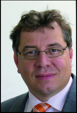
Ralf Montino

Ralf Montino
VP PLI
Elmos Semiconductor AG

Ralf Montino

Abstract
In the past, the processes “Wafer Sort”, “Assembly” and “Final Test” were considered as more or less independent processes with limited duties: Assembly should cover the silicon and the two test processes took care about the functionality of the product. Efficiency increase results from reducing test effort and increasing the parallelism of the test.Today, more and more of the products are customized during the test. This includes flashing customer specific software as well as adjustments at sometimes several temperatures. A more integrated view on these three different steps is necessary. Moreover, there are new demands to the machines. In addition to that, increasing of parallelism is very limited by the handling systems available on the market.

Biography
Study of physics in Dortmund and Aachen (high-energy physics).PHd in Engineering from the University of Siegen ( Knowledge Based Systems and Knowledge Management )With Elmos since 1990. - Started working for Elmos as a developer of test programs for the automatic electrical test of products.From the middle of the 90's development of the IT at Elmos. (There was actually nothing like that before - you can hardly imagine it today ...)Besides the office IT from the beginning, the integration of the manufacturing processes into the IT structures was a focus.After many years of responsibility for IT: Establishing a new organizational structure taking care about test program development, product engineering and assemblyThe core topics are:Broadening the supply chain, growth at the OSATSEngineering EfficiencyAnd, for shure, COT

14:35
New Approaches to Achieve Superior Reliability in Power Electronic Packaging
  Andreas Grassmann, Vice President for Package Innovation, Infineon Technologies AG
New Approaches to Achieve Superior Reliability in Power Electronic Packaging
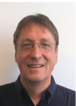

Andreas Grassmann

Andreas Grassmann
Vice President for Package Innovation
Infineon Technologies AG

Andreas Grassmann

Abstract
Coming Soon

Biography
Andreas Grassmann is currently working for Infineon Technologies AG as Vice President for package innovation with strong focus on automotive power modules. He is in semiconductor industry since more than 30 years. He was working in various management position in R&D and technology in Europe, Asia and USA. He holds a PhD in Physics from the University of Erlangen.

14:55
Bare Copper Lead Frame Compatible Die Attach Developments for Automotive Applications
  Tony Winster, Technical Advisor, Henkel Ltd
Bare Copper Lead Frame Compatible Die Attach Developments for Automotive Applications


Tony Winster

Tony Winster
Technical Advisor
Henkel Ltd

Tony Winster

Abstract
Many semiconductor devices using SOIC, QFP and QFN format are packaged by mounting and wire bonding a die onto metal lead frames using conductive die attach adhesive. Such lead frames have traditionally been fabricated from copper, with a surface of Ag or Ni-Pd-Au (PPF) plating to provide good and stable adhesion and electrical contacts. However, the elimination of the plated finishes would offer significant reduced costs; and also improved reliability, due to higher adhesion of molding compounds to the metal leadframe. To enable this trend, the die attach industry has been engaged in developing new adhesives which offer excellent compatibility with bare copper. In addition, package performance has been improved by formulating for enhanced electrical & thermal conductivity to allow higher power ratings. This has been achieved partly by using increased Ag contents, but mainly by introducing Ag sintering mechanisms. Lastly, package reliability has been improved by optimizing formulations to withstand stresses imposed by higher AEC Q100 automotive requirements, in particular passing 2000 or even more thermal cycles from -55 to 150 Celsius (Grade 0). This has been done by optimizing the polymer chemistry, but also by introducing additives to act as “crack stoppers” to absorb stresses and prevent cracks & delamination from propagating.The paper will describe how a test vehicle was selected to quantify improvements in packages, using automotive industry standard tests. And then go on to describe how changes in chemistry have been introduced to enable significant improvements to package specifications, while controlling and reducing overall package costs, and providing compatibility with materials currently adopted by multiple semiconductor makers, and maintaining capability of being processed using existing equipment and processes.This development work has produced many successes, and continues with a program of further improvements. A “roadmap” showing targeted future developments will be outlined.

Biography
Tony Winster studied Metallurgy & Materials Science before researching materials for high reliability electronics. After some years involved with design and manufacture of Defence/Aerospace packages, Tony joined Ablestik, supporting and growing their respected range of die attach materials. Since Henkel took over Ablestik in 2008, Tony is technically deeply involved with the wide portfolio of Henkel products for semiconductor packages, by supporting new semiconductor packaging developments & “design-in” programs around Europe.

15:15
High-speed Die, Component 3D Reconstruction Solution ​by Multimodal Phase Shift Optics Approach
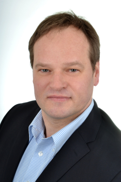

  Axel Lindloff, Senior Process Specialist Pre-Sales, Koh Young Europe GmbH
High-speed Die, Component 3D Reconstruction Solution ​by Multimodal Phase Shift Optics Approach
Axel Lindloff

Axel Lindloff
Senior Process Specialist Pre-Sales
Koh Young Europe GmbH

Axel Lindloff

Abstract
The first automated 3D inline measurement system for solder paste inspection was introduced in 2003 to the global Surface Mount Technology (SMT) industry by Koh Young Technologies. This system utilized Moiré fringe pattern technology to accurately measure pixel heights. Subsequently, 3D solder paste measurement became an established industrial standard in SMT within a few years. Building on the same measurement concept, the first automated 3D component measurement system, known as Automated Optical Inspection (AOI), was introduced in 2010. Today, 3D measurement has become the prevailing AOI standard.The packaging industry has also shown keen interest in this technology from its inception. The measurement principle proved to be robust and flexible, offering high accuracy at faster speeds compared to conventional point-measurement methods like confocal microscopy. Consequently, 3D solder paste inspection was quickly adopted for printing applications in the packaging sector.However, 3D AOI systems encountered challenges in the harsh conditions of the semiconductor packaging world. Particularly, systems based on Moiré fringe pattern technology faced difficulties with the mirroring surface of silicon chips. Moreover, the topography posed a challenge with small features, such as 0201 metric components located next to higher silicon chips in densely packed layouts.Presently, advancements in optical 3D measurement and the integration of Artificial Intelligence (AI) have paved the way for advanced packaging applications. Multi-modal measurement probes, equipped with enhanced depth of focus, are capable of covering all height differences in state-of-the-art packaging. Various surface conditions of components, chips, and surfaces are measured by combining an oblique optical system, which ensures stable high-speed measurement of objects with diffuse reflection, with a coaxial optical system, suitable for measuring objects with specular reflection. The integration of AI deep learning technology enables effective processing of various noises encountered during the measurements.In conclusion, this presentation will highlight how high-speed 3D reconstruction addresses the growing demand for electronic components, which necessitates fast and efficient processing. These advancements in measurement technology and AI integration have paved the way for enhanced packaging applications in the semiconductor industry.

Biography
Axel Lindloff pursued his studies in general electrical engineering at Bielefeld University of Applied Sciences and has been an active participant in the SMT industry since 1999. He gained initial experience in sales for a period of 3 years before transitioning to the application department of a printing machine manufacturer in 2003. During his time there until 2012, Axel focused on optimizing existing processes, conducting audits, and developing new printing applications.Since September 2012, Mr. Lindloff has been employed as a Senior Process Specialist at Koh Young Europe GmbH. His primary responsibilities revolve around process optimization using 3D data, facilitating machine-to-machine communication, conducting process audits, and contributing to the introduction of new products.

15:35
How to Achieve Upcoming Bump Requirements by Optimized ECD Plating Processes
  Stefan Pieper, Global Application Manager for Semiconductor Processes, MKS/Atotech
How to Achieve Upcoming Bump Requirements by Optimized ECD Plating Processes

Stefan Pieper
Global Application Manager for Semiconductor Processes
MKS/Atotech

Stefan Pieper

Abstract
Next to Cu-to-Cu hybrid bonding technology for upcoming packaging requirements, the rapid advancements in advanced packaging technologies demand the development of cutting-edge microbump structures with smaller pitch sizes in the range of < 10 µm. Hence, optimized electrochemical deposition (ECD) plating processes will be required to fulfill the needs for this microbump structures. This presentation focuses on the deposition of Cu, Ni-alloys and SnAg, each of them crucial for device miniaturization and performance. We will first give insights into the optimization of the process parameters to allow shape control and the simultaneous deposition of Cu bumps of different sizes on one die (i.e., “hybrid bumps”). Additionally, due to ever decreasing form factors, next generation plating requires Ni-alloy-based barrier layers, which form minimal intermetallic compounds. We will present novel results of possible barrier materials with minimized intermetallic layer thickness. The final part of the presentation focuses on SnAg plating and the optimization of coplanarity and surface roughness, other crucial bump features for smallest, next generation packages.

Biography
Stefan Pieper has studied chemistry in Berlin, Germany where he also completed his PH.D. in analytical chemistry. In 2009 he joined Atotech as Application Scientist in the department of Semiconductor Advanced Packaging processes where he used the opportunity to gain deep insight in multiple electrochemical metallization processes and their characterization for semiconductor application. During his work as Application Scientist, he also spent over 3 years in the US where he optimized Cu dual damascene electrodeposition and Through Silicon Via plating. In 2020 he took over the position as Global Application Manager for semiconductor processes at MKS/Atotech. In his current position he is leading a team that provides wet-chemical solutions for semiconductor metallization with the focus on power semiconductor.

15:55 Key Takeways from Session Chair
  Peter Cockburn, Senior Product Marketing Manager, Cohu, Inc.

Peter Cockburn
Senior Product Marketing Manager
Cohu, Inc.

Biography
Peter Cockburn is Senior Product Marketing Manager at Cohu’s Interface Solutions Group, responsible for RF contactors and probe cards. He has worked in the ATE industry for over 30 years at Schlumberger, NPTest, Credence, LTX-Credence, Xcerra and Cohu. During this time he has developed realtime and GUI software for ATE systems, launched several new SOC ATE systems and provided marketing and sales support in USA, Asia and Europe. More recently he was responsible for defining and delivering complete test cells that reduce cost of test for MEMS sensor applications. He has an Engineering degree from the University of Southampton, UK.

16:00 Coffee break
 

Session 4: SiP requirements and Advanced Packaging Solutions for Future Applications

16:40 Opening Remarks by Session Chair
  Tanja Braun, Program Director, Fraunhofer IZM

Tanja Braun

Tanja Braun
Program Director
Fraunhofer IZM

Biography
Tanja Braun studied mechanical engineering at Technical University of Berlin with a focus on polymers and micro systems and joined Fraunhofer IZM in 1999. In 2013 she received her Dr. degree from the Technical University of Berlin for the work focusing on humidity diffusion through particle-filled epoxy resins. Tanja Braun is head of the group Assembly & Encapsulation Technologies. Recent research is focused on fan-out wafer and panel level packaging technologies.

16:45
Topic Coming Soon
  Lihong Cao, Sr. Director, Engineering & Technical Marketing, ASE, Inc.
Topic Coming Soon

Lihong Cao

Lihong Cao
Sr. Director, Engineering & Technical Marketing
ASE, Inc.

Lihong Cao

Abstract
Coming Soon

Biography
Dr.Lihong Cao is Sr. Director, Engineering & Technical Marketing at ASE, with responsibility for driving advanced packaging technology development, package architecture for chiplet integration, technology promotion, new product introduction, strategic planning, and business engagement. Lihong has a proven track record of successfully leading engineering operations to bring up advanced System-in-Package production and chiplets integration. Her expertise spans across design, process development, and production enablement. Prior to joining ASE, Lihong served as a Senior Manager at AMD, leading advanced packaging technology qualification worldwide for over sixteen years. She was also responsible for 2.5D packaging technology development and led AMD advanced packaging and assembly process qualifications for cross-over for all new products. Lihong received a Ph.D. in Material Science & Engineering from Wuhan University of Technology, prior to completing tenure as a Research Associate Professor at Nanyang Technology University in Singapore. She holds more than 70 publications.

17:05
Optimization of Advanced Packaging Process: Concept of Maskless Dual–Layer Lithographic Patterning
  Ksenija Varga, Business Development Manager, EV Group
Optimization of Advanced Packaging Process: Concept of Maskless Dual–Layer Lithographic Patterning
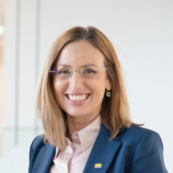

Ksenija Varga

Ksenija Varga
Business Development Manager
EV Group

Ksenija Varga

Abstract
The integration of advanced packaging features in heterogeneous integration, 3D stacking, and miniaturization of electronic devices is enabled by FO WLP. It offers several benefits, including improved electrical performance, reduced form factor, and enhanced thermal dissipation vs. conventional packaging technologies. The cost–efficient solution to the industry established dual–damascene process in the interconnect formation was investigated in the present paper in relation to the FO WLP application. For this purpose, the concept of maskless exposure patterning of the novel dielectric materials by using two exposure dose levels was set in the DoE.The lithographic patterning was performed by dual–dose exposure of VIA and RDL traces using a single coating and development step without intermediate alignment. The objective was to achieve low resolution, low dielectric layer thickness having half–thickness of the first layer in the dual exposed patterns. A newly developed, low–temperature cure positive tone polybenzoxazoles (PBO) dielectric is cured at about 200 °C and thus is compatible with epoxy materials used in FO WLP packages.The low–temperature cure dielectric was also developed for markets like MRAM, RF, MEMS, and backside RDL applications where the base substrate, other materials, or the device packages themselves are temperature sensitive and require a low–cure dielectric material.At first, an understanding of dose dependency on the dielectric penetration depth in dual–layer exposure needed to be proven. Maskless exposure technology offers a simple exposure dose/wavelength/focus matrix. The parameters can be easily adjusted via recipe enabling efficient process evaluation. The contrast curve proved the linear behavior of exposure dose vs. removed thickness layer after the development. By patterning with the most optimal dual–exposure parameters, the resolution 3.8 µm (via within via opening), min. dual–layer thickness of 8 µm (first layer thickness 4 µm) after cure was proven by SEM images and stylus profile measurement. The spectral reflectance images reveal uniform film thickness (FT) distribution after spin coating, while the FT non–uniformity increased after the cure and the development processes.In conclusion, the newly established concept can support continuous efforts of the BEOL semiconductor industry in the total cost–of–ownership optimization.

Biography
Ksenija Varga is Business Development Manager at EV Group with Head Quarter in Austria, where she is focusing on new application development for maskless exposure technology, primarily in advanced packaging and heterogenous integration. Besides business development, Ksenija is involved in strategic projects working on new lithography equipment for next-generation devices. Prior to EV Group, Ksenija was working at FujiFilm Electronic Materials. She holds a doctorate degree in Chemistry from the University of Innsbruck in Austria and has experience in R&D project management and account management.

17:25
High Efficiency Cleaning for Permanent Bonding-Based 3D Applications
  Donald Dussault, General Manager, ProSys, Inc.
High Efficiency Cleaning for Permanent Bonding-Based 3D Applications


Donald Dussault

Donald Dussault
General Manager
ProSys, Inc.

Donald Dussault

Abstract
Bond defectivity due to particle generated voids in the bond interface is a limiter in direct bonding yield. This issue is growing exponentially with the reduction in interconnect pitch making the killer defect particle size smaller and smaller. An effective cleaning process should remove all contaminates (if removeable), but must not add particulate or damage the substrates to be cleaned. The cleaning method should also be applicable to singulated die on tape frame and address the die edge/kerf contamination without displacing the die. In this presentation we will present a unique Megasonic Cleaning device that meets these emerging cleaning challenges. We will also present pre-bond cleaning results achieved with this device in several direct bonding applications evaluated both through classical particle detection (SP-X) as well as actual void detection with acoustic microscope. We will further describe how this device can be applied to the evolving cleaning challenges in W2W and D2W Hybrid bonding process sequences.

Biography
General Manager, ProSys, Inc., the market leader in Megasonic systems for the Semiconductor Industry wet process segment. Since 2005 he has successfully expanded the application range and installed base of ProSys Megasonic systems in the European and Asian markets making ProSys the de facto standard for many high volume production OEMs.Don started in the Semiconductor industry in 1980 as an Equipment Engineer responsible for a new front-end startup, and later specialized in Microlithography systems for a leading Semiconductor OEM. Don was transferred to Europe to support the rapid expansion there in the Mid 1980s and has remained in Europe ever since. For the past 20+ years he has specialized in wet process applications and has held management positions with several OEM Equipment suppliers. During this time he has helped to develop and test new wet process applications. He has co-authored papers on, and presented much of this process development work to the wet process community.

17:45 Key Takeways from Session Chair
  Tanja Braun, Program Director, Fraunhofer IZM
Tanja Braun

Tanja Braun
Program Director
Fraunhofer IZM

Biography
Tanja Braun studied mechanical engineering at Technical University of Berlin with a focus on polymers and micro systems and joined Fraunhofer IZM in 1999. In 2013 she received her Dr. degree from the Technical University of Berlin for the work focusing on humidity diffusion through particle-filled epoxy resins. Tanja Braun is head of the group Assembly & Encapsulation Technologies. Recent research is focused on fan-out wafer and panel level packaging technologies.


Session 5: Power Electronics Pack

17:50 Opening Remarks by Session Chair
  Roberto Antonicelli, Automotive BU for US and Europe, JCET Group - STATS ChipPAC

Roberto Antonicelli

Roberto Antonicelli
Automotive BU for US and Europe
JCET Group - STATS ChipPAC

Biography
Roberto Antonicelli is a professional with over 20 years of experience in the semiconductor industry. At JCET Group, formerly STATS ChipPAC, he is in charge of the Automotive BU for US and Europe. He is based in Morges (Switzerland), on the shores of the Leman Lake. Prior to joining STATS ChipPAC in 2010, he has held diverse R&D positions at Infineon Technologies, Alcatel Microelectronics and ST Microelectronics. Roberto obtained his MSEE and PhD from Polytechnic University of Bari, Italy, respectively in 1997 and 2002.

17:55
Pushing the Limits of SiC Technology: Advanced Packaging Solutions and System Integration
  Alessandro Tumminia, ADG Back End R&D Manager, STmicroelectronics
Pushing the Limits of SiC Technology: Advanced Packaging Solutions and System Integration
Alessandro Tumminia

Alessandro Tumminia
ADG Back End R&D Manager
STmicroelectronics

Abstract
The trend towards electrification in the industrial and automotive sectors is driven by the need for sustainable and energy-efficient solutions. This is leading to a shift towards wideband gap semiconductor materials such as silicon carbide (SiC) and gallium nitride (GaN) for power discretes and modules, replacing traditional silicon (Si) components.SiC and GaN offer higher efficiency, faster switching speeds, and increased power density, enabling the creation of more compact and lightweight devices. Power module design is crucial for integrating wideband gap materials like SiC, and process bricks development, such as die attach and source interconnection, is equally important for ensuring high reliability and performance.Further progress is providing power box solutions (power module integration with cooling system), rather than just power module. Attachment methodology is moving away from standard thermal interface material and towards soldering or even sintering to reduce thermal resistance and increase overall system reliability.

Biography
Alessandro Tumminia is the Back End R&D Manager for STMicroelectronics in Catania, where he is responsible for package development for power discrete and power solutions, including system in package and power modules.To address the challenges of using power modules in electric vehicles, DC-DC converters, and on-board chargers in harsh operating environments, he manages a new department within R&D that performs design verification and reliability evaluation in real-life application conditions. This enables Alessandro and his team to anticipate any possible issues related to power module operation within a real customer application.After receiving his Diploma in Electronic Engineering from the University of Palermo, he began his career in the semiconductor industry in 2002, developing several NVM technologies focused on NOR. Prior to joining STMicroelectronics, he managed a cross-functional team that executed Micron 3D NAND roadmap, delivering timely qualification for NAND flash memories and supporting the SSD/Managed NAND team and R&D in achieving their targets.

18:15
An Overview of Silicon Carbide Packaging for Power Electronics
  Ashley Lobo, Master Thesis Student, Automotive
An Overview of Silicon Carbide Packaging for Power Electronics
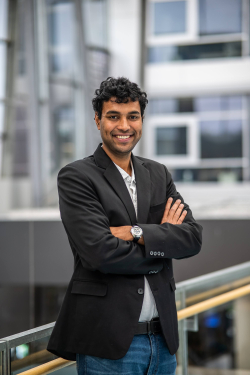
Ashley Lobo

Ashley Lobo
Master Thesis Student
Automotive

Ashley Lobo

Abstract
There has been a rise in the use of Silicon Carbide (SiC) in Power conversion applications in the photovoltaic, automotive and wind industries due to its low switching losses. This enables higher switching frequencies compared to conventional silicon devices. Recently there has been a large-scale adoption of SiC because of manufacturing breakthroughs resulting in cheaper semiconductors which can be produced on a relatively larger scale. With the shift from 150mm to 200mm wafer size, the economies of scale will be enhanced even further, leading to even greater adoption of SiC in newer industries. While SiC properties make it an ideal replacement for Si in power conversion and power electronics, to extract the full potential from SiC, innovative packaging will be required because most of the current packaging is based on Silicon and not SiC. This presentation addresses the trends, innovation, and challenges in the manufacturing of power module packaging solutions like interconnections, encapsulation, die and substrate attachment, baseplate, etc. The presentation will also analyze the manufacturing implications of new packaging topics of SiC, such shift to diode-less SiC MOSFET module from antiparallel diodes. Case studies on newer innovations like the 4-lead TO-247 Kelvin source pin by different SiC manufacturing companies will be discussed. Supply chain players of different components and their business models including product portfolio of different manufacturers, trends, and comparison of different substrate materials as well as system level trends will be evaluated. Manufacturing of newer module packaging such as the use of dual side flex foil for interconnections, substrate attachment by silver sintering of the die or newer substrates for SiC like Si3N4 and AIN will be the focus of analysis. Key requirements and innovations in packaging of SiC semiconductors from various industries like Electric Vehicles, Wind, and Photo Voltaic have been identified.AbbreviationsSiC- Silicon CarbideMOSFET- Metal oxide semiconductor field effect transistors

Biography
Ashley Lobo is a dedicated researcher and postgraduate student currently pursuing his Master's thesis at the P3 group, located in their Munich office. His research focuses on the field of semiconductors, where he explores cutting-edge advancements and contributes to the technological development of this industry. Ashley is currently enrolled in the Automotive Production Engineering program at Technische Hochschule Ingolstadt, where he deepens his knowledge and expertise in this field.Prior to his master's studies, Ashley successfully completed his undergraduate degree at Dayananda Sagar College of Engineering, Bangalore. During his time there, he demonstrated a strong passion for research and academic writing, resulting in the publication of several research papers in esteemed international journals. Additionally, he has actively participated in technical forums, showcasing his expertise by sharing insightful knowledge through more than 50 articles.

18:35 Key Takeways from Session Chair
  Roberto Antonicelli, Automotive BU for US and Europe, JCET Group - STATS ChipPAC
Roberto Antonicelli

Roberto Antonicelli
Automotive BU for US and Europe
JCET Group - STATS ChipPAC

Biography
Roberto Antonicelli is a professional with over 20 years of experience in the semiconductor industry. At JCET Group, formerly STATS ChipPAC, he is in charge of the Automotive BU for US and Europe. He is based in Morges (Switzerland), on the shores of the Leman Lake. Prior to joining STATS ChipPAC in 2010, he has held diverse R&D positions at Infineon Technologies, Alcatel Microelectronics and ST Microelectronics. Roberto obtained his MSEE and PhD from Polytechnic University of Bari, Italy, respectively in 1997 and 2002.

18:40 End of Conference
18:45 Networking Reception for Conference Participants