Wednesday, November 15, 2023
 

Session 1: Mega Trends and Opportunities for Advanced Packaging and Front-End Integration

09:00
Welcome Remarks
  Laith Altimime, President, SEMI Europe
Welcome Remarks
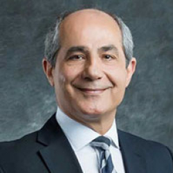
Laith Altimime

Laith Altimime
President
SEMI Europe

Laith Altimime

Abstract
Coming Soon

Biography
Laith Altimime, as President of SEMI Europe, leads SEMI’s activities in Europe and the Middle East and Africa (EMEA). Altimime has P&L responsibility as well as ownership of all Europe region programs and events, including SEMICON Europa. He is responsible for establishing industry standards, advocacy, community development, expositions, and programs. He provides support and services to SEMI members worldwide that have supply chain interests in Europe. He manages and nurtures relationships with SEMI members in the region and globally as well as with local associations and constituents in industry, government, and academia. Altimime has more than 30 years of international experience in the semiconductor industry. Prior to joining SEMI in 2015, He held senior leadership positions at NEC, KLA-Tencor, Infineon, Qimonda and imec. Altimime holds an MSc from Heriot-Watt University, Scotland.

09:20 Opening Remarks by Session Chair
  Roland Rettenmeier, Senior Product Marketing Manager, Evatec
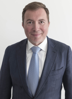
Roland Rettenmeier

Roland Rettenmeier
Senior Product Marketing Manager
Evatec

Biography
Roland Rettenmeier qualified as a Mechanical Engineer in 1997 and completed his MBA studies at Vienna, Austria in 2005. Roland extended his education through other international courses and programs since that time (e.g. Six Sigma Program with AT&S and Nokia; Innovation Technology Leader at Stanford University).Roland has worked in the field of Electronics and Semiconductor manufacturing since 2001, managing multiple international projects. After joining Evatec in 2016 as Senior Product Marketing Manager (PMM) within the Business Unit for Advanced Packaging, he focused on business development for Panel Level Packaging where Evatec has now become the recognised market leader for thin film technology solutions. Since 2020 he has also supported development of Evatec’s wafer level packaging solutions business.In addition to his market and customer responsibilities, Roland represents Evatec in the Panel Level Packaging consortium of Fraunhofer IZM Berlin, in the Packaging Research Center at Georgia Tech, USA and in the Panel Level Packaging Consortium at the NCAP in Wuxi, China.

09:25
Lights Outside Tunnel
  Douglas Yu, Vice President of TSMC R&D and TSMC Distinguished Fellow, TSMC
Lights Outside Tunnel
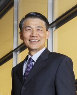
Douglas Yu

Douglas Yu
Vice President of TSMC R&D and TSMC Distinguished Fellow
TSMC

Douglas Yu

Abstract
High Performance Compute (HPC) and AI/ML have been realized by advanced nodes IC and advanced system integration technologies. Device /chip scaling and heterogeneous system integration, eg. TSMC 3DFabricTM, which consists of CoWoS®, InFO and SoIC®, become the twin engine to drive semiconductor technology. Recent new wave of generative AI with LLM showed that HPC and AI/ML have tremendous room for future growth. In the meantime, higher performance compute with higher energy efficiency become even more critical requirements than ever to support the demand. We will continue the scaling of both device/IC and advanced system in classical m-electronics based computing system. Furthermore, photonics-based system integration technology will be added which are complementary to the classical system integration to meet the ever-increasing energy efficient performance requirements for future HPC and AI/ML.

Biography
DDoug Yu is a Vice President of TSMC R&D and TSMC Distinguished Fellow, responsible for system integration technology pathfinding. Previously, Doug has pioneered and led TSMC Cu/Low-K technology development, industry first wafer-level system integration technology platform, TSMC 3DFabricTM, including CoWoS®, InFO and SoICTM, and TSMC COUPE, a photonics-based system integration technology.Prior to TSMC, Doug worked with AT&T Bell Labs. He received Ph.D. degree in Materials Science and Engineering from Georgia Institute of Technology, Atlanta, GA.Doug is a recipient of IEEE Rao Tummala Award, IEEE EPS Microelectronics Manufacturing Award, and President Science Prize, Taiwan. He is an IEEE Fellow, TSMC Distinguished Fellow, and a member of National Academy of Engineering. He has given numerous invited/keynote/plenary speeches in international conferences and published 150+ papers to elevate system integration technology profile. He has (co)-authored 1500+ US granted semiconductor technology patents.

09:45
Latest Solutions in the Energy Efficiency of Electronic Systems
  Hannes Voraberger, Corporate Vice President R&D, AT&S Austria Technologie & Systemtechnik Aktiengesellschaft
Latest Solutions in the Energy Efficiency of Electronic Systems
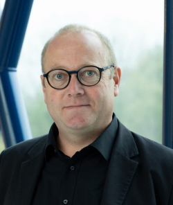
Hannes Voraberger

Hannes Voraberger
Corporate Vice President R&D
AT&S Austria Technologie & Systemtechnik Aktiengesellschaft

Hannes Voraberger

Abstract
Digitalization without further improvement in the energy efficiency of electronic systems will lead to a dramatic increase in energy requirements for data processing. The solution is based on processing systems with smaller nodes and a highly efficient power supply. Interconnect technology based on advanced IC substrate technologies offer great opportunities for improved signal processing and efficient power supply. Latest solutions will be presented in this talk.

Biography
Dr. Voraberger assumed his current position in 2010, as head of AT&S corporate research and development department. Previously Dr. Voraberger was responsible for AT&S corporate intellectual property and governmental funding.He also established the R&D center in AT&S Shanghai (China) and was project leader for AT&S research and development in AT&S Leoben (Austria).Dr. Voraberger studied industrial chemistry at Graz University of Technology, awarded multiple patents and has published several papers.

10:05 Coffee break
10:45 Reserved
11:05 Reserved
11:25 Key Takeways from Session Chair
  Roland Rettenmeier, Senior Product Marketing Manager, Evatec
Roland Rettenmeier

Roland Rettenmeier
Senior Product Marketing Manager
Evatec

Biography
Roland Rettenmeier qualified as a Mechanical Engineer in 1997 and completed his MBA studies at Vienna, Austria in 2005. Roland extended his education through other international courses and programs since that time (e.g. Six Sigma Program with AT&S and Nokia; Innovation Technology Leader at Stanford University).Roland has worked in the field of Electronics and Semiconductor manufacturing since 2001, managing multiple international projects. After joining Evatec in 2016 as Senior Product Marketing Manager (PMM) within the Business Unit for Advanced Packaging, he focused on business development for Panel Level Packaging where Evatec has now become the recognised market leader for thin film technology solutions. Since 2020 he has also supported development of Evatec’s wafer level packaging solutions business.In addition to his market and customer responsibilities, Roland represents Evatec in the Panel Level Packaging consortium of Fraunhofer IZM Berlin, in the Packaging Research Center at Georgia Tech, USA and in the Panel Level Packaging Consortium at the NCAP in Wuxi, China.


Session 2: Smarter Supply Chain Solutions for a Sustainable Ecosystem

11:30 Opening Remarks by Session Chair
  Ruby Yan, Globalfoundries

Ruby Yan

Globalfoundries

11:35
Environmental Footprint Chip Manufacturing
  Cedric Rolin, Program Manager Sustainable Electronics, imec
Environmental Footprint Chip Manufacturing
Cedric Rolin

Cedric Rolin
Program Manager Sustainable Electronics
imec

Cedric Rolin

Abstract
Coming Soon

Biography
Coming Soon

11:55
The Future of Advanced Packaging Inspection is X-Ray!
  Isabella Drolz, Vice President Product Marketing, Comet Yxlon GmbH
The Future of Advanced Packaging Inspection is X-Ray!
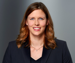
Isabella Drolz

Isabella Drolz
Vice President Product Marketing
Comet Yxlon GmbH

Isabella Drolz

Abstract
The global demand for high-end computing power driven by smartphones, IoT applications, High-performance computing, and new mobility applications is constantly rising while facing miniaturization demands. The semiconductor industry is all about identifying and solving these challenges and thereby, yield and process control is core for foundries and its importance increased even more through the introduction of advanced packaging.In today’s environment two things can be observed. One, prototyping and verification costs exponentially increase while node sizes decrease. Two, a change from typical inspection methods like optical or FIB-SEM to advanced non-destructive inspection techniques like X-ray inspection.Ultimately advanced packaging companies seek non-destructive automated inspection tools which are fast enough to provide value within their production processes, increase yield and reduce waste at an early stage. This presentation will give an overview on how X-Ray and CT inspection can provide value-added data and information for exactly that.

Biography
Isabella Drolz is the Vice President Product Marketing at Comet Yxlon, which is the industrial X-ray & CT inspection system division of Comet. Comet Yxlon provides X-ray & CT inspection solutions for R&D labs & production environments, especially for Semiconductor customers to enhance their productivity. In her role she is responsible for product management, business development, global application solution centers and marketing at Comet Yxlon. Isabella has next to her industrial engineering education, a Bachelor of Science in International Business Administration and a MBA degree from Southern Nazarene University in Oklahoma City, USA. She has held several management positions in the mechanical and plant engineering industry driving market-oriented product development.

12:15
Director Process Design Semiconductor Materials
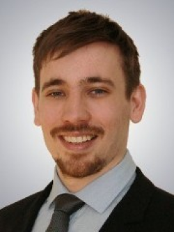
  Thorsten vom Stein, Merck Electronics KGaA
Director Process Design Semiconductor Materials
Thorsten vom Stein

Thorsten vom Stein

Merck Electronics KGaA

Thorsten vom Stein

Abstract
The drive to scale nodes towards physical limits, known as "More than Moore", and the adoption of 3D architecture in chip integration strategies for advanced logic and memory applications has led to an unprecedented demand for high-quality and dependable materials solutions. This presentation focuses on the digitalization of chemical process design for semiconductor materials manufacturing, employing molecular precision. It delves into the data-driven approaches used to streamline manufacturing processes from laboratory to HVM scale by leveraging connected asset infrastructures for cost optimization, quality, reliability, and sustainable excellence. Moreover, this talk emphasizes the importance of diversity and inclusion in fostering the "leap of faith" culture necessary for this digital revolution.

Biography
Professional ExperienceSince January 2022 Director, Head of Process Design Semiconductor MaterialsJune 2020 - January 2022 Director, Head of Process Development Semiconductor Materials EuropeJan. 2018 - May 2020 Associate Director Process Technology Japan, Chemical Lead of ProcessDevelopment Performance Materials Asia (Expatriate Assignment)Jul. 2015 – Dec. 2017Laboratory Head at Merck KGaA Process DevelopmentMarch 2014 - July 2015 Alexander-von-Humboldt Foundation research fellow (Feodor Lynen program) in the group of Professor D. W. Stephan at the University of TorontoEducationOctober 2010 – March 2014 PhD thesis (summa cum laude) “Catalytic Multistep Hydrogenation andHydrogenolysis Reactions for the Utilization of Renewable Carbon Resources”’ in the group of Professor W. Leitner as part of the cluster of excellence „Tailor Made Fuels from Biomass“ (TMFB) at the ITMC, RWTH Aachen UniversityAugust 2010 Graduation diploma (Dipl.-Chem.) in chemistry with distinction (summa cum laude)Diploma thesis “Organic acid catalyzed selective fractionation of lignocellulose” in the group of Professor W. Leitner as part of the cluster of excellence „Tailor MadeFuels from Biomass“ at the Institut für Technische und Makromolekulare Chemie(ITMC), RWTH Aachen University2005-2010 Undergraduate studies in chemistry at RWTH Aachen University 2005 High school diploma1996-2005 High school education at the Städtisches Gymnasium Wermelskirchen

12:35 Key Takeways from Session Chair
  Ruby Yan, Globalfoundries

Ruby Yan

Globalfoundries

12:40 Networking Lunch
 

Session 3: Testing, Reliability and Materials

13:40 Opening Remarks by Session Chair
13:45
It is all about Cost of Test? New Duties for Packaging and Test
  Ralf Montino, VP PLI, Elmos Semiconductor AG
It is all about Cost of Test? New Duties for Packaging and Test
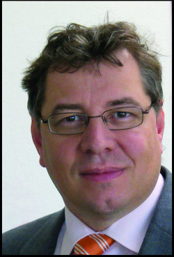
Ralf Montino

Ralf Montino
VP PLI
Elmos Semiconductor AG

Ralf Montino

Abstract
In the past, the processes “Wafer Sort”, “Assembly” and “Final Test” were considered as more or less independent processes with limited duties: Assembly should cover the silicon and the two test processes took care about the functionality of the product. Efficiency increase results from reducing test effort and increasing the parallelism of the test.Today, more and more of the products are customized during the test. This includes flashing customer specific software as well as adjustments at sometimes several temperatures. A more integrated view on these three different steps is necessary. Moreover, there are new demands to the machines. In addition to that, increasing of parallelism is very limited by the handling systems available on the market.

Biography
Study of physics in Dortmund and Aachen (high-energy physics).PHd in Engineering from the University of Siegen ( Knowledge Based Systems and Knowledge Management )With Elmos since 1990. - Started working for Elmos as a developer of test programs for the automatic electrical test of products.From the middle of the 90's development of the IT at Elmos. (There was actually nothing like that before - you can hardly imagine it today ...)Besides the office IT from the beginning, the integration of the manufacturing processes into the IT structures was a focus.After many years of responsibility for IT: Establishing a new organizational structure taking care about test program development, product engineering and assemblyThe core topics are:Broadening the supply chain, growth at the OSATSEngineering EfficiencyAnd, for shure, COT

14:05
Topic Coming Soon
  Andreas Grassmann, Vice President, Infineon Technologies AG
Topic Coming Soon

Andreas Grassmann

Andreas Grassmann
Vice President
Infineon Technologies AG

Andreas Grassmann

Abstract
Coming Soon

Biography
Coming Soon

14:25 Reserved
14:45 Reserved
15:05
How to Achieve Upcoming Bump Requirements by Optimized ECD Plating Processes
  Stefan Pieper, Global Application Manager for Semiconductor Processes, MKS/Atotech
How to Achieve Upcoming Bump Requirements by Optimized ECD Plating Processes

Stefan Pieper
Global Application Manager for Semiconductor Processes
MKS/Atotech

Stefan Pieper

Abstract
Next to Cu-to-Cu hybrid bonding technology for upcoming packaging requirements, the rapid advancements in advanced packaging technologies demand the development of cutting-edge microbump structures with smaller pitch sizes in the range of < 10 µm. Hence, optimized electrochemical deposition (ECD) plating processes will be required to fulfill the needs for this microbump structures. This presentation focuses on the deposition of Cu, Ni-alloys and SnAg, each of them crucial for device miniaturization and performance. We will first give insights into the optimization of the process parameters to allow shape control and the simultaneous deposition of Cu bumps of different sizes on one die (i.e., “hybrid bumps”). Additionally, due to ever decreasing form factors, next generation plating requires Ni-alloy-based barrier layers, which form minimal intermetallic compounds. We will present novel results of possible barrier materials with minimized intermetallic layer thickness. The final part of the presentation focuses on SnAg plating and the optimization of coplanarity and surface roughness, other crucial bump features for smallest, next generation packages.

Biography
Stefan Pieper has studied chemistry in Berlin, Germany where he also completed his PH.D. in analytical chemistry. In 2009 he joined Atotech as Application Scientist in the department of Semiconductor Advanced Packaging processes where he used the opportunity to gain deep insight in multiple electrochemical metallization processes and their characterization for semiconductor application. During his work as Application Scientist, he also spent over 3 years in the US where he optimized Cu dual damascene electrodeposition and Through Silicon Via plating. In 2020 he took over the position as Global Application Manager for semiconductor processes at MKS/Atotech. In his current position he is leading a team that provides wet-chemical solutions for semiconductor metallization with the focus on power semiconductor.

15:25 Reserved
15:45 Reserved
16:05 Key Takeways from Session Chair
16:10 Coffee break
 

Session 4: SiP requirements and Advanced Packaging solutions for future applications

16:50 Opening Remarks by Session Chair
  Tanja Braun, Fraunhofer IZM

Tanja Braun

Fraunhofer IZM

16:55 Reserved
17:15 Reserved
17:35 Key Takeways from Session Chair
  Tanja Braun, Fraunhofer IZM

Tanja Braun

Fraunhofer IZM


Session 5: Power Electronics Pack