Wednesday, November 15, 2023
 

Session 1: Fab Expansion Landscape: Opportunities and Challenges

08:30
Welcome Remarks
  Laith Altimime, President, SEMI Europe
Welcome Remarks
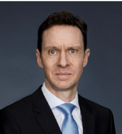
Laith Altimime

Laith Altimime
President
SEMI Europe

Laith Altimime

Abstract
Coming Soon

Biography
Laith Altimime, as President of SEMI Europe, leads SEMI’s activities in Europe and the Middle East and Africa (EMEA). Altimime has P&L responsibility as well as ownership of all Europe region programs and events, including SEMICON Europa. He is responsible for establishing industry standards, advocacy, community development, expositions, and programs. He provides support and services to SEMI members worldwide that have supply chain interests in Europe. He manages and nurtures relationships with SEMI members in the region and globally as well as with local associations and constituents in industry, government, and academia. Altimime has more than 30 years of international experience in the semiconductor industry. Prior to joining SEMI in 2015, He held senior leadership positions at NEC, KLA-Tencor, Infineon, Qimonda and imec. Altimime holds an MSc from Heriot-Watt University, Scotland.

08:40
The Great Wolfspeed Takeover
  Missy Stigall, SVP Global Fab Operations, Wolfspeed
The Great Wolfspeed Takeover
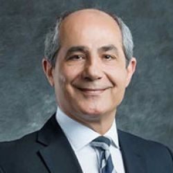
Missy Stigall

Missy Stigall
SVP Global Fab Operations
Wolfspeed

Missy Stigall

Abstract
Coming Soon

Biography
Missy is responsible for the strategy and direction of the Wolfspeed global device factories, developing innovative production solutions, building dynamic manufacturing and engineering teams, and delivering on-time quality execution that meets customer needs. In addition, she sponsors our Management of Change initiative, is responsible for several initiatives in the Global Ops organization, and has a passion for driving critical conversations that result in solutions that evolve inclusion and diversity.Missy has 25 years of experience in the semiconductor industry, encompassing a wide range of roles. She graduated from Southern Methodist University with a BS in Electrical Engineering and from Kettering University with a MS in Engineering Management.

09:00 Opening Remarks by Session Chair
  Joerg Recklies, Senior Vice President, Infineon Technologies AG
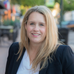
Joerg Recklies

Joerg Recklies
Senior Vice President
Infineon Technologies AG

Biography
Joerg Recklies has been in the semiconductor industry for 27 years with responsibilities ranging from Chip design to IDM. He is currently in charge of the General Manager at Infineon Technologies Regensburg. Prior to that, Joerg Recklies was in charge of the FAB Manager at Infineon Dresden and held several positions in automation and productions at Infineon. These positions contributed to his excellent experience in terms of equipment and automation. Earlier in his carrier he has made contributions in digital and analog Chip design.Joerg Recklies holds a graduate engineer for Semiconductor. Highlight during the time with Infineon …. - Establish high automation at IFD 1995- 1997 as project leader automation software integration- Project Leader world wide cost reduction program within Infineon Frontend Productions from 1999 –2003 (within Europe, US, Asia)- Section Manager Plasma Etch / Wafer Inspection 2003- 2007- Director Maintenance Engineering 2007 – 2014- Project Leader 300 mm Fab Startup / Transfer Power Technologies 2011-2013- FAB Manager Senior Director 200 / 300 mm Dresden 2014 – 2018- General Manager Site Regensburg Senior Vice President since 2018

09:05
Building the new Smart Power Fab in Dresden: A Strong Signal for the Future
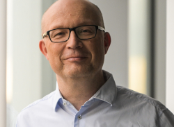
  Holger Hasse, Project Manager for the Plant Expansion, nfineon Site Dresden, Infineon Technologies Dresden GmbH
Building the new Smart Power Fab in Dresden: A Strong Signal for the Future
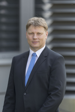
Holger Hasse

Holger Hasse
Project Manager for the Plant Expansion, nfineon Site Dresden
Infineon Technologies Dresden GmbH

Holger Hasse

Abstract
The Infineon Dresden production site already produces over 400 different products based on 200- and 300-millimeter wafers. The site was founded in 1994 – at that time still as part of Siemens.Today, Infineon operates one of the most modern and largest sites for manufacturing, technology, and product development in Dresden – with around 3,300 employees. This makes Infineon Dresden one of the largest industrial employers in the region.With the new Smart Power Fab, the site in Dresden will grow significantly in the coming years and become Infineon’s largest Frontend location. This investment is an essential contribution to achieving the European Commission’s declared objective of reaching a 20 percent share of global semiconductor production in the EU by 2030. Semiconductor solutions for industrial and automotive applications from the Dresden Fab will help secure value chains in key European industries even better in the future.The Smart Power Fab is the largest single investment in Infineon’s corporate history and will make a decisive contribution to driving climate protection and digitalization forward. With the level of digitalization and automation established here, Infineon in Dresden is also setting new standards in manufacturing excellence. Furthermore about 1,000 direct new jobs will be created.In February 2023, the Infineon Management Board and supervisory bodies gave the green light for the Dresden site. The German Federal Ministry for Economic Affairs and Climate Action (BMWK) has approved an early project launch, meaning that construction can already begin before completion of the inspection of legal subsidy aspects by the European Commission. Subject to the European Commission's state aid decision and the national grant procedure, the project is to be funded in accordance with the objectives of the European Chips Act.For a long time, no semiconductor plant of this size was built in Europe. Due to the increasing demand in the semiconductor market, Infineon has set a very ambitious timeline for this complex project. Diverse challenges arise, for example, the extensive approval process with the local authorities must be mastered. Price increases in construction and delays in delivery of long lead items must also be absorbed.

Biography
As Senior Project Director at Infineon Dresden, Holger Hasse is responsible for the construction and facilitation of the new Smart Power Fab with more than 20,000-square-meter clean room, where the 300-millimeter wafers for semiconductor production will be processed in the future.He learned the semiconductor business from scratch: At the beginning of the 1990s, he completed an apprenticeship as an electronics technician and started in the industry in 1995. At the same time, he studied business administration and mechanical engineering.After his studies, Holger Hasse first took care of maintenance as a team leader and later as a department manager. This was followed by management positions in various production areas at different semiconductor companies.Holger Hasse was born in Görlitz, Germany, in 1970.

09:25
Discover Saxony-Anhalt - Vibrant Industries Joined by Intel’s Gigafactories
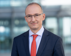
  Robert Franke, Managing Director, IMG – Investment and Marketing Corporation Saxony-Anhalt
Discover Saxony-Anhalt - Vibrant Industries Joined by Intel’s Gigafactories
Robert Franke

Robert Franke
Managing Director
IMG – Investment and Marketing Corporation Saxony-Anhalt

Robert Franke

Abstract
Saxony-Anhalt, operating on a global scale, is soon home to global players like Intel, Daimler, Avnet, and Sioux. Discover the possibilities of our region, which is on the path to becoming a leading European high-tech area and also offers a solid base of small and medium-sized companies.

Biography
Since January 2023, Robert Franke is Managing Director of IMG – Investment and Marketing Corporation Saxony-Anhalt.Before Robert Franke was Director Office of Economic Development and Director Office of Road and Infrastructure Department (temp.) in City of DresdenFrom 2013 to 2016, Robert Franke was Managing Director of Energy Saxony e.V.

09:35 Key Takeways from Session Chair
  Joerg Recklies, Senior Vice President, Infineon Technologies AG
Joerg Recklies

Joerg Recklies
Senior Vice President
Infineon Technologies AG

Biography
Joerg Recklies has been in the semiconductor industry for 27 years with responsibilities ranging from Chip design to IDM. He is currently in charge of the General Manager at Infineon Technologies Regensburg. Prior to that, Joerg Recklies was in charge of the FAB Manager at Infineon Dresden and held several positions in automation and productions at Infineon. These positions contributed to his excellent experience in terms of equipment and automation. Earlier in his carrier he has made contributions in digital and analog Chip design.Joerg Recklies holds a graduate engineer for Semiconductor. Highlight during the time with Infineon …. - Establish high automation at IFD 1995- 1997 as project leader automation software integration- Project Leader world wide cost reduction program within Infineon Frontend Productions from 1999 –2003 (within Europe, US, Asia)- Section Manager Plasma Etch / Wafer Inspection 2003- 2007- Director Maintenance Engineering 2007 – 2014- Project Leader 300 mm Fab Startup / Transfer Power Technologies 2011-2013- FAB Manager Senior Director 200 / 300 mm Dresden 2014 – 2018- General Manager Site Regensburg Senior Vice President since 2018


Session 2: Industrial Collaboration Models

09:50 Opening Remarks by Session Chair
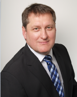
  Mario von Podewils, Director MEMS & Erfurt Operations, X-FAB Semiconductor Foundries GmbH
Mario von Podewils

Mario von Podewils
Director MEMS & Erfurt Operations
X-FAB Semiconductor Foundries GmbH

Biography
Mario von Podewils has more than 40 years of experience in microelectronics manufacturing. In 1982, he started his career as a maintenance technician for various types of semiconductor manufacturing equipment in the microelectronics industry in Erfurt, Germany. After obtaining his degree in electronics engineering, he spent several years as a team leader responsible for equipment maintenance in various process areas in wafer fabrication at Thesys GmbH, Erfurt. From 1992 to 2001, he was project manager of national and international joint projects in the semiconductor industry, mainly funded by the BMBF or the EU.In 2001, he obtained his diploma in industrial engineering, specialising in operations and production management. Since then, he has held various positions as department and module manager for equipment engineering and the lithography module at X-FAB Semiconductor Foundries AG, among others. In 2007, he took over the position of Fab Operations Manager at X-FAB Semiconductor Foundries GmbH in Erfurt.At the beginning of 2021, he was delegated to the MEMS site in Itzehoe of the XFAB Group as Site Manager. Since autumn 2022, as Director MEMS & Erfurt Operations, he is now responsible for both wafer fabs at the Erfurt and Itzehoe sites as well as X-FAB's global MEMS production.

09:55
Challenges of Capacity Doubling Under Brownfield and Full Load Conditions
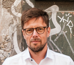
  Michael Woittennek, CEO X-FAB Dresden, X-FAB Dresden GmbH & Co. KG
Challenges of Capacity Doubling Under Brownfield and Full Load Conditions
Michael Woittennek

Michael Woittennek
CEO X-FAB Dresden
X-FAB Dresden GmbH & Co. KG

Michael Woittennek

Abstract
Coming Soon

Biography
Michael Woittennek is CEO - Managing Director, X-FAB Dresden GmbH & Co. KG with a strong focus on cooperation and growth of the teams during the last 15 years in X-FAB. Responsibility for Dresden location including and ~580 employees in operations, facility, quality, controlling, IT and R&D. Short- and long-term goal- and priority setting responsibility. Focus on economy of scale activities (ramp 11.000 wafer starts/month) and clear support of automation roadmap to improve profitability of the site.

10:15 Coffee break
10:55
The Advanced APC Application to Enable the Geometric Scaling by DTCO in sub-5nm SoC Manufacturing
  Leo Kim, Principal Engineer, Qualcomm Korea
The Advanced APC Application to Enable the Geometric Scaling by DTCO in sub-5nm SoC Manufacturing
Leo Kim

Leo Kim
Principal Engineer
Qualcomm Korea

Leo Kim

Abstract
Moore’s law gets slower down by the limitation of physical scaling down in sub-10nm technology and it is essential to design the new products associated with DTCO (Design-Technology Co-Optimization). The recent approaches with non-active area scale-down demonstrated the significant contribution to reduce std-cell track but it can cause the narrow process window which was not fully caught by DFM (Design for Manufacturing) and NPI verification. To effectively bring up DTCO in HPC (High Performance Computing) devices, the inline F/F (feedforward) APC was adopted to assure the product quality on the top of the conventional APC F/B (feedback) for R2R control. However, the upgraded APC was not sufficient to meet the requirements of products qualities across wafers and dies in case of UHD cell structure. The newly developed APC system could achieve Snapdragon 888 mobile platform HVM in time by introducing wafer-level as well as within-wafer zonal APC. At the next step, the real-time APC by VM of tool sensors, the extended e-beam application and ML (Machine Learning) will greatly reduce TTD (Time to Detect).

Biography
Leo Kim is a Principal Eng. in Foundry Engineering team at Qualcomm Korea. He is currently responsible for foundry management/process technology development to deliver Qualcomm mobile platform solutions into worldwide market across leading-edge FinFET technologies. He joined Qualcomm Inc., Korea in 2009, bringing over 20 years of semiconductor BiCMOS/CMOS R&D device & process integration experiences from Samsung Electronics Co., Chartered Semiconductor of Singapore, IBM alliance members in USA. His role has been extended to unit process, device design, process architecture development and product manufacturing technology delivery. He has a MS in electrical engineering from Yonsei University, Korea.

11:15 Reserved
11:35 Key Takeways by Session Chair
  Mario von Podewils, Director MEMS & Erfurt Operations, X-FAB Semiconductor Foundries GmbH
Mario von Podewils

Mario von Podewils
Director MEMS & Erfurt Operations
X-FAB Semiconductor Foundries GmbH

Biography
Mario von Podewils has more than 40 years of experience in microelectronics manufacturing. In 1982, he started his career as a maintenance technician for various types of semiconductor manufacturing equipment in the microelectronics industry in Erfurt, Germany. After obtaining his degree in electronics engineering, he spent several years as a team leader responsible for equipment maintenance in various process areas in wafer fabrication at Thesys GmbH, Erfurt. From 1992 to 2001, he was project manager of national and international joint projects in the semiconductor industry, mainly funded by the BMBF or the EU.In 2001, he obtained his diploma in industrial engineering, specialising in operations and production management. Since then, he has held various positions as department and module manager for equipment engineering and the lithography module at X-FAB Semiconductor Foundries AG, among others. In 2007, he took over the position of Fab Operations Manager at X-FAB Semiconductor Foundries GmbH in Erfurt.At the beginning of 2021, he was delegated to the MEMS site in Itzehoe of the XFAB Group as Site Manager. Since autumn 2022, as Director MEMS & Erfurt Operations, he is now responsible for both wafer fabs at the Erfurt and Itzehoe sites as well as X-FAB's global MEMS production.


Session 4: Cultivating the Workforce of Tomorrow

11:40 Opening Remarks by Session Chair
  Cassandra Melvin, Senior Director of Business Development & Operations, SEMI Europe
Cassandra Melvin

Cassandra Melvin
Senior Director of Business Development & Operations
SEMI Europe

Biography
Cassandra joined SEMI Europe in 2018 to lead its operations, business development and strategic initiatives related to diversity and inclusion. In this role she is responsible for leading a culturally diverse team, enhancing member value, and directing operations for optimized financial performance. Prior to joining SEMI, she held the position Global Product Manager at Atotech for its semiconductor division. She began her career at the SUNY Polytechnic Institute as a Business Manager focused on technical programs for chemistry and equipment manufacturers and held project management roles in clean room operations and IT. Cassandra's written work has been published in leading technical magazines and presented at conferences globally. She holds a BS in Business Management, and Minor in Neuropsychology from Rensselaer Polytechnic Institute.

11:45
Topic Coming Soon
  Bernard Capraro, EU Talent Development Programme Manager, Intel Research and Development Ireland Ltd
Topic Coming Soon
Bernard Capraro

Bernard Capraro
EU Talent Development Programme Manager
Intel Research and Development Ireland Ltd

Bernard Capraro

Abstract
Coming Soon

Biography
Bernie received a Masters Degree in Engineering from Newcastle upon Tyne Polytechnic (now Northumbria University Newcastle) and has been working at Intel for the past 26 years holding various Engineering and Management roles across the wafer fabrication facilities, semiconductor and nanotechnology research activities in Ireland and wider Europe, as well as University engagement and relationship building across Ireland. Bernie is currently responsible for Higher Education talent pipeline development across wider Europe, currently focusing on Intel’s manufacturing expansions in Germany and Poland. In February 2019, Bernie was announced as an Adjunct Professor within Ireland’s first Technological University, TU Dublin. Bernie’s semiconductor experience spans 36 years, with other Process and Equipment Engineering positions held at Telefunken GmbH (DE), Nortel/Bell Northern Research (UK/Canada), Applied Materials (UK) and Newport Wafer Fab (UK).

12:05 Panel discussion

Achieving EU Ambitions through Successful Recruitment and Retention

Moderation Cassandra Melvin, Senior Director of Business Development & Operations, SEMI Europe
Cassandra Melvin

Cassandra Melvin
Senior Director of Business Development & Operations
SEMI Europe

Cassandra Melvin

Biography
Cassandra joined SEMI Europe in 2018 to lead its operations, business development and strategic initiatives related to diversity and inclusion. In this role she is responsible for leading a culturally diverse team, enhancing member value, and directing operations for optimized financial performance. Prior to joining SEMI, she held the position Global Product Manager at Atotech for its semiconductor division. She began her career at the SUNY Polytechnic Institute as a Business Manager focused on technical programs for chemistry and equipment manufacturers and held project management roles in clean room operations and IT. Cassandra's written work has been published in leading technical magazines and presented at conferences globally. She holds a BS in Business Management, and Minor in Neuropsychology from Rensselaer Polytechnic Institute.

Panelists
  • Flemming Kehr, Global Practice Lead, Sustainability, Mercuri Urval
  • Flemming Kehr

    Flemming Kehr
    Global Practice Lead, Sustainability
    Mercuri Urval

    Flemming Kehr

    Biography
    More than 25 years of experience in advising leading international organisations and innovative start-ups. Deep understanding and knowledge of strategydevelopment and implementation, fit-for-future programmes, leadership development programmes, leadership framework development, performanceacceleration as well as on building purpose-and value-driven leadership teams and organisations. Strong focus, experience and interest in sustainabilityleadership, DEIB-leadership and on how to merge sustainability and circularity with strategy.

  • Bernard Capraro, EU Talent Development Programme Manager, Intel Research and Development Ireland Ltd
  • Bernard Capraro

    Bernard Capraro
    EU Talent Development Programme Manager
    Intel Research and Development Ireland Ltd

    Bernard Capraro

    Biography
    Bernie received a Masters Degree in Engineering from Newcastle upon Tyne Polytechnic (now Northumbria University Newcastle) and has been working at Intel for the past 26 years holding various Engineering and Management roles across the wafer fabrication facilities, semiconductor and nanotechnology research activities in Ireland and wider Europe, as well as University engagement and relationship building across Ireland. Bernie is currently responsible for Higher Education talent pipeline development across wider Europe, currently focusing on Intel’s manufacturing expansions in Germany and Poland. In February 2019, Bernie was announced as an Adjunct Professor within Ireland’s first Technological University, TU Dublin. Bernie’s semiconductor experience spans 36 years, with other Process and Equipment Engineering positions held at Telefunken GmbH (DE), Nortel/Bell Northern Research (UK/Canada), Applied Materials (UK) and Newport Wafer Fab (UK).

12:45 Networking Lunch
 

Session 5: Solutions Enabling the Path to Net-Zero

13:45 Opening Remarks by Session Chair
  Klaus Schimpf, Fab Manager, Texas Instruments
Klaus Schimpf

Klaus Schimpf
Fab Manager
Texas Instruments

Biography
Now 25 years with TI- 1997: Phd in Physics Research Centre Juelich- 1997: joining TI in Freising as Product engineer working on Development and yield improvement of Annalog technologies- 2007-2020: various mgmt roles in Engineering and Operations- 2021: Fab Manager , FFAB TI Freising

13:50
TI’s Energy Saving Activities
  Alexander Stur, Facilities Engineering Manager, Texas Instruments
TI’s Energy Saving Activities
Alexander Stur

Alexander Stur
Facilities Engineering Manager
Texas Instruments

Alexander Stur

Abstract
Coming Soon

Biography
Coming Soon

14:10
Why Digital Solutions are the Key to a Sustainable Fab Transformation
  Sharon Hua, Global Strategy Director Semiconductor Segment, Schneider Electric
Why Digital Solutions are the Key to a Sustainable Fab Transformation
Sharon Hua

Sharon Hua
Global Strategy Director Semiconductor Segment
Schneider Electric

Sharon Hua

Abstract
The climate crisis we face today is the result of how we, as businesses, organizations, governments, and individuals, make decisions. Semiconductor CAPEX grew by 21% to a record of $185.5billion in 2022. This growth lines up a potential challenge to the international climate goals. Both the EU and US aim to get halfway to net zero carbon emissions by 2030, and to net zero by 2050. And as the semiconductor industry grows, so too will its carbon footprint.To reduce carbon emissions, we must decide to consume less energy and use energy more efficiently in our semiconductor manufacturing. It sounds simple. But we all know that this involves often unpopular decisions: Making it happen is tough. Especially without the right data. The good news is that today’s digital technologies can help us make decisions smarter, faster, more precisely – all of which is ultimately better for the planet. We will discuss the 3 enablers we use to support semiconductor industry on climate, from strategy to execution.

Biography
Global Director of Strategy & BD for Semiconductor SegmentGlobal Director of Strategy & BD for Semiconductor SegmentJan 2021 - Present · 2 yrs 7 mosJan 2021 - Present · 2 yrs 7 mosStrategy & BD managerStrategy & BD managerJan 2018 - Dec 2020 · 3 yrsJan 2018 - Dec 2020 · 3 yrs中国 江苏省 无锡中国 江苏省 无锡Strategy & BD manager, in Power Product BUStrategy & BD manager, in Power Product BUDigital strategy deployment managerDigital strategy deployment managerMay 2014 - Jan 2018 · 3 yrs 9 mosMay 2014 - Jan 2018 · 3 yrs 9 mos中国 上海市中国 上海市Digital strategy deployment

14:30
Continuous Sustainability Improvements in Subfab Operation Using Advanced Communication Capabilities as a Cooperative Effort of Multiple Stakeholders
  Andreas Neuber, Semior Director, Applied Materials GmbhH
Continuous Sustainability Improvements in Subfab Operation Using Advanced Communication Capabilities as a Cooperative Effort of Multiple Stakeholders

Andreas Neuber
Semior Director
Applied Materials GmbhH

Abstract
Provision of signals from process to subfab components have shown for some time the potential for a more sustainable operation of subfab equipment such as local abatement, dry pumps and others. This accounts to about 20% of the overall equivalent energy consumption of the manufacturing.The drive to transition to carbon neutrality in fab operation asks for further improvements.The presentation will address which optimization potentials have been identified and what needs to be done to implement them.A lot of them will require cross-functional efforts over many disciplines. Smart manufacturing methods are playing a very important part in the implementation as well.

Biography
Andreas Neuber, Ph.D. has been a Senior Director at Applied Materials since 2008. He has published 80+ papers related to semiconductor fab and facility design, sustainable design and energy savings, water management and recycling, contamination control, and industrial engineering.Prior to joining Applied Materials, Andreas Neuber was Vice President for M+W Zander. During his 18 years at M+W Zander, was involved in semiconductor fab construction and operation/optimization in many locations.Andreas Neuber received a PhD degree in Chemical Engineering from University of Technology Dresden. He is co-chair of the SEMI ESEC task force as well as Co-Chair for the IRDS Yield Enhancement Gas working group and the IRDS ESH/S Energy working group.

14:50
Watlow’s Approach Towards Energy Efficiency and Achieving Net-Zero
  Blake Parkinson, Director of Gas Delivery Business Segment, Watlow Electric Manufacturing Company
Watlow’s Approach Towards Energy Efficiency and Achieving Net-Zero
Blake Parkinson

Blake Parkinson
Director of Gas Delivery Business Segment
Watlow Electric Manufacturing Company

Blake Parkinson

Abstract
Watlow’s Lean Journey began more than 15 years ago. As we began to implement changes, we quickly learned that this journey would not just improve our manufacturing efforts, but that it would also be the start of our own Green Journey. As a company, we have undertaken many initiatives to reduce our footprint including improvements in HVAC efficiency, lighting, and release of pollutants. Our main initiative is to join many companies in the world and achieve net-zero emissions in 2050 or before. As a supplier to many of the world's leading companies, Watlow is also committed to supporting our customers’ Green Journey. Using unique raw materials, computer-aided simulations, and advanced power control technology, we can ensure that the right amount of heat is applied to the right location and at the right time. Provides our customers with the ability to realize at least a 10% reduction in power output. Which, when scaled to fab-level consumption, provides meaningful support to our worldwide journey to net-zero emissions.

Biography
Blake Parkinson has gained a Master in Business (MBA) and Master in Chemical engineering. He has been with Watlow for 8 years, served in several roles in Operations, Project Management, Process Engineering, and Business Management. Blake has global experience in new product development, supplier development, and cross-functional team leadership. His current role is Director of Gas Delivery and Exhaust in the Semiconductor business unit.

15:10 Key Takeways from Session Chair
  Klaus Schimpf, Fab Manager, Texas Instruments
Klaus Schimpf

Klaus Schimpf
Fab Manager
Texas Instruments

Biography
Now 25 years with TI- 1997: Phd in Physics Research Centre Juelich- 1997: joining TI in Freising as Product engineer working on Development and yield improvement of Annalog technologies- 2007-2020: various mgmt roles in Engineering and Operations- 2021: Fab Manager , FFAB TI Freising

15:15 Coffee break
 

Session 6: Smarter Manufacturing for a Connected Ecosystem

16:10 Opening Remarks by Session Chair
  Simone Alba, AG300 Fab - CVD and Dry Etch Area Manager, STMicroelectronics
Simone Alba

Simone Alba
AG300 Fab - CVD and Dry Etch Area Manager
STMicroelectronics

Biography
Coming Soon

16:15
The Future of Advanced Packaging Inspection is X-Ray
  Dionys van de Ven, President of the Industrial X-Ray Systems (IXS) Division, Comet Yxlon
The Future of Advanced Packaging Inspection is X-Ray
Dionys van de Ven

Dionys van de Ven
President of the Industrial X-Ray Systems (IXS) Division
Comet Yxlon

Dionys van de Ven

Abstract
Key take aways:- Semiconductor industry is driven by miniaturization & efficiency- Next generation X-Ray as valuable inspection method for Advanced packaging- X-Ray as booster for faster time-to-market & increased yieldIn Summary:X-Ray technology is ready as a valuable inspection solution for Advanced Packaging to reduce time-to-market and increase yield.

Biography
Dionys van de VenPresident Industrial X-Ray Systems Born 1968, Dutch citizen; Master’s degree in mechanical engineering from the Eindhoven University of Technology, EindhovenBefore joining Comet in 2022, Dionys van de Ven has led Waygate Technologies’ x-ray business unit (part of Baker Hughes) as the unit’s Business Executive since 2020. In addition, he has been serving as Managing Director of Baker Hughes Digital Solutions GmbH and member of the board of management of GE Inspection Robotics.Dionys van de Ven began his career at Philips Assembléon in 1997. In 2005 he became Director of Customer Relationship Management at Philips Applied Technologies and, in 2007, Senior Director of Customer Programs, Service and R&D at Philips Healthcare. In 2017, he joined Waygate Technologies.

16:35
Wafer Intelligent Scanner Inspection Technology
  Marco Franchi, Sales Marketing Executive, Tokyo Electron Europe Limited
Wafer Intelligent Scanner Inspection Technology
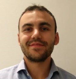
Marco Franchi

Marco Franchi
Sales Marketing Executive
Tokyo Electron Europe Limited

Marco Franchi

Abstract
Coming Soon

Biography
Marco has more than 5 years of experience in the Semiconductors industry. Upon his graduation in Chemical Engineering from Politecnico di Milano (Italy) in Milan, Marco joined GE (General Electric) in 2017 for the Water Business branch. In 2018 he has moved to Tokyo Electron, serving as Sales Marketing Executive for the Clean Track Business Unit in Europe.Marco works closely with the Customers and the Factory, implementing projects for new systems and improvements into Europe business.Marco has more than 5 years of experience in the Semiconductors industry. Upon his graduation in Chemical Engineering from Politecnico di Milano (Italy) in Milan, Marco joined GE (General Electric) in 2017 for the Water Business branch. In 2018 he has moved to Tokyo Electron, serving as Sales Marketing Executive for the Clean Track Business Unit in Europe.Marco works closely with the Customers and the Factory, implementing projects for new systems and improvements into Europe business.Marco has more than 5 years of experience in the Semiconductors industry. Upon his graduation in Chemical Engineering from Politecnico di Milano (Italy) in Milan, Marco joined GE (General Electric) in 2017 for the Water Business branch. In 2018 he has moved to Tokyo Electron, serving as Sales Marketing Executive for the Clean Track Business Unit in Europe.Marco works closely with the Customers and the Factory, implementing projects for new systems and improvements into Europe business.Marco has more than 5 years of experience in the Semiconductors industry. Upon his graduation in Chemical Engineering from Politecnico di Milano (Italy) in Milan, Marco joined GE (General Electric) in 2017 for the Water Business branch. In 2018 he has moved to Tokyo Electron, serving as Sales Marketing Executive for the Clean Track Business Unit in Europe.Marco works closely with the Customers and the Factory, implementing projects for new systems and improvements into Europe business.

16:55
Enabling Semi's Autonomous Fab
  John Behnke, General Manager FPS Product Line, INFICON
Enabling Semi's Autonomous Fab
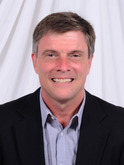
John Behnke

John Behnke
General Manager FPS Product Line
INFICON

John Behnke

Abstract
Coming Soon

Biography
Mr. Behnke has over 35 years of semiconductor industry experience including: logic and memory manufacturing, technology/product development and fab operational excellence. As the GM of Final Phase Systems an INFICON Product Line, John leads a team that develop and deploy SMART software solutions that enable fabs to improve their manufacturing efficiency. FPS’s suite of software solutions are built upon a common Datawarehouse which enables advanced Fab Scheduling and optimized WIP movement as well as other related capabilities. He is also a Co-Chair of the Semi North America Smart Manufacturing Special Interest Group. Prior to FPS John served as the CEO and President of Novati Technologies, the SVP and GM of the Semiconductor Group of Intermolecular, the CVP for Front End Manufacturing, Process R&D and Technology Transfers at Spansion and the Director of AMD’s Fab 25’s Engineering and Operations groups where he was a founding member of AMD’s Automated Precision Manufacturing (APM) initiative which led the Semiconductor industry’s development and use of APC and other advanced factory systems. He also led the successful conversion of Fab 25 from Logic to Flash memory which was enabled through the virtual automation of the fab.Mr. Behnke earned a B.S. degree in Mechanical Engineering with an Industrial Engineering Minor from Marquette University. Mr. Behnke holds five U.S. patents.

17:15
Squeezing More Wafers out of a Fab: Can this be Done without Driving Cycle Times Through the Roof?
  Peter Lendermann, Chief Business Development Officer, D-SIMLAB Technologies
Squeezing More Wafers out of a Fab: Can this be Done without Driving Cycle Times Through the Roof?
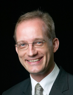
Peter Lendermann

Peter Lendermann
Chief Business Development Officer
D-SIMLAB Technologies

Peter Lendermann

Abstract
Despite the current dip in global IC demand in some areas, industry leaders are optimistic about mid- and long-term growth prospects in semiconductor manufacturing which is also illustrated by the large number of new wafer fabrication facilities that are already under construction or being planned across the globe.In this setting, optimisation of factory capacity – with the objective to squeeze even more wafers out of existing fabs – will continue to be a critical challenge. To achieve this, powerful techniques to determine fab load mixes that are able to maximise wafers out – or better revenue, or even much better margin – with existing capacity are essential. At the same time, because of the complex operating curve of a wafer fab it is important to precent cycle times from going through the roof to make sure that delivery performance to customers does not suffer. In an environment with fast-changing customer demand and product mixes, as well as frequent commissioning of new equipment this is not an easy task at all.How such load mix optimisation can be achieved through a combination of static and dynamic (simulation-enabled) capacity models and powerful yet intelligent optimisation techniques will be showcased in this presentation. Enhancement of the wafer out potential by a double-digit percentage without exceeding operationally feasible equipment utilisation limits and without compromising cycle time has been demonstrated with multiple semiconductor manufacturing companies.

Biography
Peter Lendermann is a Co-Founder and the Chief Business Development Officer of D-SIMLAB Technologies, a Singapore-headquartered company providing simulation-based decision support solutions to Semiconductor Manufacturing companies. Prior to this he worked at the Singapore Institute of Manufacturing Technology where he led related R&D activities until spinning them off into D-SIMLAB. Peter has been engaged in the field of production logistics, supply chain management and related decision support technologies and solutions since the early 1990’s. He holds a PhD in Physics from Humboldt University in Berlin (Germany) and an MBA in International Economics and Management from SDA Bocconi in Milan (Italy).

17:35
Topic to be confirmed soon
  Jamie Potter, Co-founder and CEO, Flexciton Ltd
Topic to be confirmed soon
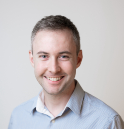
Jamie Potter

Jamie Potter
Co-founder and CEO
Flexciton Ltd

Jamie Potter

Abstract
Abstract to be delivered soon

Biography
Jamie Potter, CEO and Co-founder, FlexcitonJamie is passionate about solving the hardest industrial problems. For the past 10 years, he has been developing optimisation solutions for various sectors, with a focus on semiconductor manufacturing. As an entrepreneur at heart, after spending a few years working in an industrial consultancy, Jamie co-founded Flexciton in 2016. He was initially directly involved in developing and implementing the first release of Flexciton scheduling software at the Seagate Springtown wafer fab. Along with his role as the company CEO, Jamie leads the commercial and operations teams. Over the past 7 years, Jamie has worked on over a dozen operational improvement projects with various semiconductor manufacturers. Jamie is a smart manufacturing enthusiast with an ambition to bring new technology to the semiconductor industry to enable new levels of efficiency.Jamie has graduated with honours in MMath from Oxford University, UK. In 2018 he was featured in Forbes' “30 under 30 list”.

17:55
Combining Physical and Virtual Metrology for Adaptive Process Control
  Christian Hörr, Business Development Manager, ZEISS Digital Innovation
Combining Physical and Virtual Metrology for Adaptive Process Control
Christian Hörr

Christian Hörr
Business Development Manager
ZEISS Digital Innovation

Christian Hörr

Abstract
Virtual metrology, i.e. predicting workpiece characteristics by means of dense machine and process parameter time series, be it simulated or recorded real-world data, has become common practice in a wide range of applications in semiconductor manufacturing. However, these process twins tend to be quantitatively inaccurate and/or they decalibrate over time, especially when either process parameters such as environmental conditions are difficult to control or the influences themselves as well as their interplay are largely unknown. This often causes complex and error-prone correlation procedures and intralogistics. Even if process stability is finally mastered, expert knowledge is increasingly difficult to scale and therefore a permanent structural risk.In this talk, we present a generic closed-loop approach how to combine physical and virtual metrology to shift the limits of precision manufacturing in terms of accuracy. Following the ultimate goal of autonomous production, we are also able to massively reduce process ramp-up and cycle times, increase the degree of automation, and finally learn how to transfer process twins to other setups. Using brownfield examples from metal machining, we demonstrate the feasibility of the approach with a technology-agnostic, software-driven solution, including machine-integrated sensors and optical scanners, containerized edge computing modules, and cloud-based datalakes. It turns out that neither physical nor virtual metrology can solve the problem on its own, but each of them relaxes the technical and non-technical requirements on the other.

Biography
2011: PhD in Computer Science from Chemnitz University of Technology2011-2015: Software Engineer and Head of Software Development at Steinbichler Optotechnik2015-2021: Head of Software Development and Head of Automation (ad interim) at ZEISS Optotechniksince 2021: Business Development Manager and Program Manager at ZEISS Digital Innovation

18:15
Smarter Manufacturing for a Connected Ecosystem
  Peter Buseck, Director IT & Automation, Robert Bosch GmbH
Smarter Manufacturing for a Connected Ecosystem
Peter Buseck

Peter Buseck
Director IT & Automation
Robert Bosch GmbH

Peter Buseck

Abstract
Ecosystem of Bosch Semiconductor Plant Reutlingen is separated in several dimensions. Dealing with 150mm and 200mm on one side as well as an 800 recipe process flow distributed over four buildings and different building levels are just two aspects. Operating manufacturing processes for wafers and diced components, tracing products from waferstart to final test including external assembly partners are additional aspects. Smart solutions in Digitalisation and Automation can lead to a connected ecosystem for all of these dimensions.This session will show current activities in Digitalisation and Automation at Bosch Semiconductor Plant Reutlingen driven by strong expansion of manufacturing area. Main focus is how smart projects and innovative solutions lead to a virtual and physical connection of a distributed and separated ecosystem.

Biography
1997: Diploma Business Engineering, University Siegen1997: Robert Bosch GmbH, Semiconductor Plant Reutlingen2009: Robert Bosch Elektronika Kft., Manufacturing Plant Hatvan Hungary2012: Robert Bosch GmbH, Semiconductor Plant Reutlingensince 2014 responsible for IT & Automation

18:35 Key Takeways from Session Chair
  Simone Alba, AG300 Fab - CVD and Dry Etch Area Manager, STMicroelectronics
Simone Alba

Simone Alba
AG300 Fab - CVD and Dry Etch Area Manager
STMicroelectronics

Biography
Coming Soon

18:40 Networking Reception for Conference Participants