Wednesday, November 15, 2023
 

Session 1: Fab Expansion Landscape: Opportunities and Challenges

08:30
Welcome Remarks
  Laith Altimime, SEMI Europe
Welcome Remarks
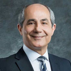
Laith Altimime

Laith Altimime

SEMI Europe

Laith Altimime

Abstract
Coming Soon

Biography
Laith Altimime, as President of SEMI Europe, leads SEMI’s activities in Europe and the Middle East and Africa (EMEA). Altimime has P&L responsibility as well as ownership of all Europe region programs and events, including SEMICON Europa. He is responsible for establishing industry standards, advocacy, community development, expositions, and programs. He provides support and services to SEMI members worldwide that have supply chain interests in Europe. He manages and nurtures relationships with SEMI members in the region and globally as well as with local associations and constituents in industry, government, and academia. Altimime has more than 30 years of international experience in the semiconductor industry. Prior to joining SEMI in 2015, He held senior leadership positions at NEC, KLA-Tencor, Infineon, Qimonda and imec. Altimime holds an MSc from Heriot-Watt University, Scotland.

08:50
Opening Remarks
  Joerg Recklies, Infineon Technologies AG
Opening Remarks
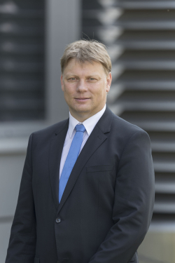
Joerg Recklies

Joerg Recklies

Infineon Technologies AG

Joerg Recklies

Abstract
Coming Soon

Biography
Joerg Recklies has been in the semiconductor industry for 27 years with responsibilities ranging from Chip design to IDM. He is currently in charge of the General Manager at Infineon Technologies Regensburg. Prior to that, Joerg Recklies was in charge of the FAB Manager at Infineon Dresden and held several positions in automation and productions at Infineon. These positions contributed to his excellent experience in terms of equipment and automation. Earlier in his carrier he has made contributions in digital and analog Chip design.Joerg Recklies holds a graduate engineer for Semiconductor. Highlight during the time with Infineon …. - Establish high automation at IFD 1995- 1997 as project leader automation software integration- Project Leader world wide cost reduction program within Infineon Frontend Productions from 1999 –2003 (within Europe, US, Asia)- Section Manager Plasma Etch / Wafer Inspection 2003- 2007- Director Maintenance Engineering 2007 – 2014- Project Leader 300 mm Fab Startup / Transfer Power Technologies 2011-2013- FAB Manager Senior Director 200 / 300 mm Dresden 2014 – 2018- General Manager Site Regensburg Senior Vice President since 2018

08:55
Topic Coming Soon
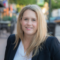
  Missy Stigall, SVP Global Fab Operations, Wolfspeed
Topic Coming Soon
Missy Stigall

Missy Stigall
SVP Global Fab Operations
Wolfspeed

Missy Stigall

Abstract
Coming Soon

Biography
Missy is responsible for the strategy and direction of the Wolfspeed global device factories, developing innovative production solutions, building dynamic manufacturing and engineering teams, and delivering on-time quality execution that meets customer needs. In addition, she sponsors our Management of Change initiative, is responsible for several initiatives in the Global Ops organization, and has a passion for driving critical conversations that result in solutions that evolve inclusion and diversity.Missy has 25 years of experience in the semiconductor industry, encompassing a wide range of roles. She graduated from Southern Methodist University with a BS in Electrical Engineering and from Kettering University with a MS in Engineering Management.

09:15
Building the new Smart Power Fab in Dresden: A Strong Signal for the Future
  Holger Hasse, Infineon Technologies Dresden GmbH
Building the new Smart Power Fab in Dresden: A Strong Signal for the Future
Holger Hasse

Holger Hasse

Infineon Technologies Dresden GmbH

Holger Hasse

Abstract
The Infineon Dresden production site already produces over 400 different products based on 200- and 300-millimeter wafers. The site was founded in 1994 – at that time still as part of Siemens.Today, Infineon operates one of the most modern and largest sites for manufacturing, technology, and product development in Dresden – with around 3,300 employees. This makes Infineon Dresden one of the largest industrial employers in the region.With the new Smart Power Fab, the site in Dresden will grow significantly in the coming years and become Infineon’s largest Frontend location. This investment is an essential contribution to achieving the European Commission’s declared objective of reaching a 20 percent share of global semiconductor production in the EU by 2030. Semiconductor solutions for industrial and automotive applications from the Dresden Fab will help secure value chains in key European industries even better in the future.The Smart Power Fab is the largest single investment in Infineon’s corporate history and will make a decisive contribution to driving climate protection and digitalization forward. With the level of digitalization and automation established here, Infineon in Dresden is also setting new standards in manufacturing excellence. Furthermore about 1,000 direct new jobs will be created.In February 2023, the Infineon Management Board and supervisory bodies gave the green light for the Dresden site. The German Federal Ministry for Economic Affairs and Climate Action (BMWK) has approved an early project launch, meaning that construction can already begin before completion of the inspection of legal subsidy aspects by the European Commission. Subject to the European Commission's state aid decision and the national grant procedure, the project is to be funded in accordance with the objectives of the European Chips Act.For a long time, no semiconductor plant of this size was built in Europe. Due to the increasing demand in the semiconductor market, Infineon has set a very ambitious timeline for this complex project. Diverse challenges arise, for example, the extensive approval process with the local authorities must be mastered. Price increases in construction and delays in delivery of long lead items must also be absorbed.

Biography
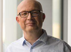
As Senior Project Director at Infineon Dresden, Holger Hasse is responsible for the construction and facilitation of the new Smart Power Fab with more than 20,000-square-meter clean room, where the 300-millimeter wafers for semiconductor production will be processed in the future.He learned the semiconductor business from scratch: At the beginning of the 1990s, he completed an apprenticeship as an electronics technician and started in the industry in 1995. At the same time, he studied business administration and mechanical engineering.After his studies, Holger Hasse first took care of maintenance as a team leader and later as a department manager. This was followed by management positions in various production areas at different semiconductor companies.Holger Hasse was born in Görlitz, Germany, in 1970.

09:35
Key Takeaways by Session Chair
  Joerg Recklies, Infineon Technologies AG
Key Takeaways by Session Chair
Joerg Recklies

Joerg Recklies

Infineon Technologies AG

Abstract
Coming Soon

Biography
Coming Soon


Session 2: Industrial Collaboration Models

09:40
Opening Remarks
  Mario von Podewils, X-FAB Semiconductor Foundries GmbH
Opening Remarks
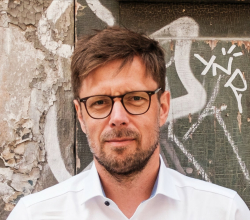
Mario von Podewils

Mario von Podewils

X-FAB Semiconductor Foundries GmbH

Mario von Podewils

Abstract
Coming Soon

Biography
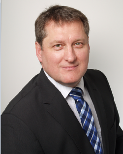
Mario von Podewils has more than 40 years of experience in microelectronics manufacturing. In 1982, he started his career as a maintenance technician for various types of semiconductor manufacturing equipment in the microelectronics industry in Erfurt, Germany. After obtaining his degree in electronics engineering, he spent several years as a team leader responsible for equipment maintenance in various process areas in wafer fabrication at Thesys GmbH, Erfurt. From 1992 to 2001, he was project manager of national and international joint projects in the semiconductor industry, mainly funded by the BMBF or the EU.In 2001, he obtained his diploma in industrial engineering, specialising in operations and production management. Since then, he has held various positions as department and module manager for equipment engineering and the lithography module at X-FAB Semiconductor Foundries AG, among others. In 2007, he took over the position of Fab Operations Manager at X-FAB Semiconductor Foundries GmbH in Erfurt.At the beginning of 2021, he was delegated to the MEMS site in Itzehoe of the XFAB Group as Site Manager. Since autumn 2022, as Director MEMS & Erfurt Operations, he is now responsible for both wafer fabs at the Erfurt and Itzehoe sites as well as X-FAB's global MEMS production.

09:45
Challenges of Capacity Doubling Under Brownfield and Full Load Conditions
  Michael Woittennek, X-FAB Dresden GmbH & Co. KG
Challenges of Capacity Doubling Under Brownfield and Full Load Conditions
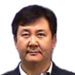
Michael Woittennek

Michael Woittennek

X-FAB Dresden GmbH & Co. KG

Michael Woittennek

Abstract
Coming Soon

Biography
Michael Woittennek is CEO - Managing Director, X-FAB Dresden GmbH & Co. KG with a strong focus on cooperation and growth of the teams during the last 15 years in X-FAB. Responsibility for Dresden location including and ~580 employees in operations, facility, quality, controlling, IT and R&D. Short- and long-term goal- and priority setting responsibility. Focus on economy of scale activities (ramp 11.000 wafer starts/month) and clear support of automation roadmap to improve profitability of the site.

10:05 Coffee break
10:45
The advanced APC application to enable the geometric scaling by DTCO in sub-5nm SoC manufacturing
  Leo Kim, Qualcomm Korea
The advanced APC application to enable the geometric scaling by DTCO in sub-5nm SoC manufacturing
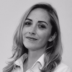
Leo Kim

Leo Kim

Qualcomm Korea

Leo Kim

Abstract
Moore’s law gets slower down by the limitation of physical scaling down in sub-10nm technology and it is essential to design the new products associated with DTCO (Design-Technology Co-Optimization). The recent approaches with non-active area scale-down demonstrated the significant contribution to reduce std-cell track but it can cause the narrow process window which was not fully caught by DFM (Design for Manufacturing) and NPI verification. To effectively bring up DTCO in HPC (High Performance Computing) devices, the inline F/F (feedforward) APC was adopted to assure the product quality on the top of the conventional APC F/B (feedback) for R2R control. However, the upgraded APC was not sufficient to meet the requirements of products qualities across wafers and dies in case of UHD cell structure. The newly developed APC system could achieve Snapdragon 888 mobile platform HVM in time by introducing wafer-level as well as within-wafer zonal APC. At the next step, the real-time APC by VM of tool sensors, the extended e-beam application and ML (Machine Learning) will greatly reduce TTD (Time to Detect).

Biography
Leo Kim is a Principal Eng. in Foundry Engineering team at Qualcomm Korea. He is currently responsible for foundry management/process technology development to deliver Qualcomm mobile platform solutions into worldwide market across leading-edge FinFET technologies. He joined Qualcomm Inc., Korea in 2009, bringing over 20 years of semiconductor BiCMOS/CMOS R&D device & process integration experiences from Samsung Electronics Co., Chartered Semiconductor of Singapore, IBM alliance members in USA. His role has been extended to unit process, device design, process architecture development and product manufacturing technology delivery. He has a MS in electrical engineering from Yonsei University, Korea.

11:05
Reserved Presentation
  Reserved Slot, _ _
Reserved Presentation

Reserved Slot

_ _

Abstract
Coming Soon

Biography
Coming Soon

11:25 Key Takeways from Session Chair, Mario von Podewils, X-Fab
 

Session 3: New Innovators – Poster Session

11:30 Poster Session – Industry meets Innovative Ideas
12:00 Networking Lunch
 

Session 4: Cultivating the Workforce of Tomorrow

13:00
Opening Remarks
  Cassandra Melvin, SEMI Europe
Opening Remarks
Cassandra Melvin

Cassandra Melvin

SEMI Europe

Cassandra Melvin

Abstract
Coming Soon

Biography
Cassandra joined SEMI Europe in 2018 to lead its operations, business development and strategic initiatives related to diversity and inclusion. In this role she is responsible for leading a culturally diverse team, enhancing member value, and directing operations for optimized financial performance. Prior to joining SEMI, she held the position Global Product Manager at Atotech for its semiconductor division. She began her career at the SUNY Polytechnic Institute as a Business Manager focused on technical programs for chemistry and equipment manufacturers and held project management roles in clean room operations and IT. Cassandra's written work has been published in leading technical magazines and presented at conferences globally. She holds a BS in Business Management, and Minor in Neuropsychology from Rensselaer Polytechnic Institute.

13:05
Reserved Presentation
  Reserved Slot, _ _
Reserved Presentation

Reserved Slot

_ _

Abstract
Coming Soon

Biography
Coming Soon

13:25 Panel discussion
13:55 Key Takeways from Session Chair, Cassandra Melvin, SEMI Europe
 

Session 5: Solutions Enabling the Path to Net-Zero

14:00
Opening Remarks
  Klaus Schimpf, Texas Instruments
Opening Remarks
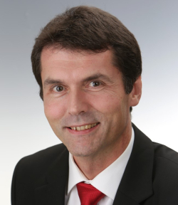
Klaus Schimpf

Klaus Schimpf

Texas Instruments

Klaus Schimpf

Abstract
Coming Soon

Biography
Now 25 years with TI- 1997: Phd in Physics Research Centre Juelich- 1997: joining TI in Freising as Product engineer working on Development and yield improvement of Annalog technologies- 2007-2020: various mgmt roles in Engineering and Operations- 2021: Fab Manager , FFAB TI Freising

14:05
TI’s Path to Net Zero Activities
  Alexander Stur, Texas Instruments
TI’s Path to Net Zero Activities
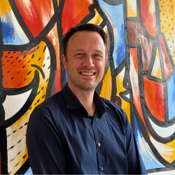
Alexander Stur

Alexander Stur

Texas Instruments

Alexander Stur

Abstract
Coming Soon

Biography
Coming Soon

14:25
Topic Coming Soon
  Andreas Neuber, Applied Materials
Topic Coming Soon

Andreas Neuber

Applied Materials

Abstract
Coming Soon

Biography
Coming Soon

14:45
Reserved Presentation
  Reserved Slot, _ _
Reserved Presentation

Reserved Slot

_ _

Abstract
Coming Soon

Biography
Coming Soon

15:05
Watlow’s approach towards energy efficiency and achieving net-zero
  Blake Parkinson, Watlow Electric Manufacturing Company
Watlow’s approach towards energy efficiency and achieving net-zero
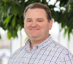
Blake Parkinson

Blake Parkinson

Watlow Electric Manufacturing Company

Blake Parkinson

Abstract
Watlow’s Lean Journey began more than 15 years ago. As we began to implement changes, we quickly learned that this journey would not just improve our manufacturing efforts, but that it would also be the start of our own Green Journey. As a company, we have undertaken many initiatives to reduce our footprint including improvements in HVAC efficiency, lighting, and release of pollutants. Our main initiative is to join many companies in the world and achieve net-zero emissions in 2050 or before. As a supplier to many of the world's leading companies, Watlow is also committed to supporting our customers’ Green Journey. Using unique raw materials, computer-aided simulations, and advanced power control technology, we can ensure that the right amount of heat is applied to the right location and at the right time. Provides our customers with the ability to realize at least a 10% reduction in power output. Which, when scaled to fab-level consumption, provides meaningful support to our worldwide journey to net-zero emissions.

Biography
Blake Parkinson has gained a Master in Business (MBA) and Master in Chemical engineering. He has been with Watlow for 8 years, served in several roles in Operations, Project Management, Process Engineering, and Business Management. Blake has global experience in new product development, supplier development, and cross-functional team leadership. His current role is Director of Gas Delivery and Exhaust in the Semiconductor business unit.

15:25 Key Takeways from Session Chair, Klaus Schimpf, Texas Instruments
15:30 Coffee break
 

Session 6: Smarter Manufacturing for a Connected Ecosystem

16:10
Opening Remarks
  Simone Alba, AG300 Fab - CVD and Dry Etch Area Manager, STMicroelectronics
Opening Remarks
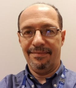
Simone Alba

Simone Alba
AG300 Fab - CVD and Dry Etch Area Manager
STMicroelectronics

Simone Alba

Abstract
Not available

Biography
Simone Alba has more than 25 years of experience in the semiconductor industry. He got his master’s degree in Physics with specialization in Plasma Physics at University of Milan. After few years spent in the field of plasmas for space applications, he joined STMicroelectronics at Agrate Brianza site (Italy). Holding various managerial roles, he had the opportunity to develop a wide technical experience in technology nodes (350-32nm), technology devices (Flash Memories, Phase Change Memories, Embedded Memories, BCD, …), manufacturing environments (from early R&D to high volume manufacturing). He also had the chance to deal with different company cultures and businesses thanks to strategic projects, technology transfers, benchmarks, etc. At present he is CVD/dry etch area manager in the new 300 mm fab in Agrate.

16:15
Topic Coming Soon
  Peter Buseck, Robert Bosch GmbH
Topic Coming Soon
Peter Buseck

Peter Buseck

Robert Bosch GmbH

Peter Buseck

Abstract
Coming Soon

Biography
Coming Soon

16:35
The Future of Advanced Packaging Inspection is X-Ray
  Dionys van de Ven, Comet
The Future of Advanced Packaging Inspection is X-Ray
Dionys van de Ven

Dionys van de Ven

Comet

Dionys van de Ven

Abstract
Key take aways:- Semiconductor industry is driven by miniaturization & efficiency- Next generation X-Ray as valuable inspection method for Advanced packaging- X-Ray as booster for faster time-to-market & increased yieldIn Summary:X-Ray technology is ready as a valuable inspection solution for Advanced Packaging to reduce time-to-market and increase yield.

Biography
Dionys van de VenPresident Industrial X-Ray Systems Born 1968, Dutch citizen; Master’s degree in mechanical engineering from the Eindhoven University of Technology, EindhovenBefore joining Comet in 2022, Dionys van de Ven has led Waygate Technologies’ x-ray business unit (part of Baker Hughes) as the unit’s Business Executive since 2020. In addition, he has been serving as Managing Director of Baker Hughes Digital Solutions GmbH and member of the board of management of GE Inspection Robotics.Dionys van de Ven began his career at Philips Assembléon in 1997. In 2005 he became Director of Customer Relationship Management at Philips Applied Technologies and, in 2007, Senior Director of Customer Programs, Service and R&D at Philips Healthcare. In 2017, he joined Waygate Technologies.

16:55
Squeezing more wafers out of a fab: Can this be done without driving cycle times through the roof?
  Peter Lendermann, D-SIMLAB Technologies
Squeezing more wafers out of a fab: Can this be done without driving cycle times through the roof?
Peter Lendermann

Peter Lendermann

D-SIMLAB Technologies

Peter Lendermann

Abstract
Despite the current dip in global IC demand in some areas, industry leaders are optimistic about mid- and long-term growth prospects in semiconductor manufacturing which is also illustrated by the large number of new wafer fabrication facilities that are already under construction or being planned across the globe.In this setting, optimisation of factory capacity – with the objective to squeeze even more wafers out of existing fabs – will continue to be a critical challenge. To achieve this, powerful techniques to determine fab load mixes that are able to maximise wafers out – or better revenue, or even much better margin – with existing capacity are essential. At the same time, because of the complex operating curve of a wafer fab it is important to precent cycle times from going through the roof to make sure that delivery performance to customers does not suffer. In an environment with fast-changing customer demand and product mixes, as well as frequent commissioning of new equipment this is not an easy task at all.How such load mix optimisation can be achieved through a combination of static and dynamic (simulation-enabled) capacity models and powerful yet intelligent optimisation techniques will be showcased in this presentation. Enhancement of the wafer out potential by a double-digit percentage without exceeding operationally feasible equipment utilisation limits and without compromising cycle time has been demonstrated with multiple semiconductor manufacturing companies.

Biography
Peter Lendermann is a Co-Founder and the Chief Business Development Officer of D-SIMLAB Technologies, a Singapore-headquartered company providing simulation-based decision support solutions to Semiconductor Manufacturing companies. Prior to this he worked at the Singapore Institute of Manufacturing Technology where he led related R&D activities until spinning them off into D-SIMLAB. Peter has been engaged in the field of production logistics, supply chain management and related decision support technologies and solutions since the early 1990’s. He holds a PhD in Physics from Humboldt University in Berlin (Germany) and an MBA in International Economics and Management from SDA Bocconi in Milan (Italy).

17:15
Topic Coming Soon
  John Behnke, INFICON
Topic Coming Soon
John Behnke

John Behnke

INFICON

John Behnke

Abstract
Coming Soon

Biography
Mr. Behnke has over 35 years of semiconductor industry experience including: logic and memory manufacturing, technology/product development and fab operational excellence. As the GM of Final Phase Systems an INFICON Product Line, John leads a team that develop and deploy SMART software solutions that enable fabs to improve their manufacturing efficiency. FPS’s suite of software solutions are built upon a common Datawarehouse which enables advanced Fab Scheduling and optimized WIP movement as well as other related capabilities. He is also a Co-Chair of the Semi North America Smart Manufacturing Special Interest Group. Prior to FPS John served as the CEO and President of Novati Technologies, the SVP and GM of the Semiconductor Group of Intermolecular, the CVP for Front End Manufacturing, Process R&D and Technology Transfers at Spansion and the Director of AMD’s Fab 25’s Engineering and Operations groups where he was a founding member of AMD’s Automated Precision Manufacturing (APM) initiative which led the Semiconductor industry’s development and use of APC and other advanced factory systems. He also led the successful conversion of Fab 25 from Logic to Flash memory which was enabled through the virtual automation of the fab.Mr. Behnke earned a B.S. degree in Mechanical Engineering with an Industrial Engineering Minor from Marquette University. Mr. Behnke holds five U.S. patents.

17:35
Reserved Presentation
  Reserved Slot, _ _
Reserved Presentation

Reserved Slot

_ _

Abstract
Coming Soon

Biography
Coming Soon

18:00
Key Takeaways by Session Chair
  Simone Alba, AG300 Fab - CVD and Dry Etch Area Manager, STMicroelectronics
Key Takeaways by Session Chair
Simone Alba

Simone Alba
AG300 Fab - CVD and Dry Etch Area Manager
STMicroelectronics

Abstract
Coming Soon

Biography
Coming Soon

18:05 End of Conference
Thursday, November 16, 2023
 

Coffee Break

14:30 tesrt