Thursday, November 17, 2022
 

Opening Keynotes

10:00
Welcome Note
  Laith Altimime, President, SEMI Europe
Welcome Note
Laith Altimime

Laith Altimime
President
SEMI Europe

Laith Altimime

Abstract
Welcome Note

Biography
As President of SEMI Europe, Laith Altimime leads SEMI’s activities in Europe and the Middle East and Africa (EMEA). Altimime has P&L responsibility as well as ownership of all Europe region programs and events, including SEMICON Europa. He is responsible for establishing industry Standards, advocacy, community development, expositions, and programs. He provides support and services to SEMI members worldwide that have supply chain interests in Europe. He manages and nurtures relationships with SEMI members in the region and globally as well as with local associations and constituents in industry, government, and academia. Altimime has more than 30 years of international experience in the semiconductor industry. Prior to joining SEMI in 2015, He held senior leadership positions at NEC, KLA-Tencor, Infineon, Qimonda and imec.Altimime holds an MSc from Heriot-Watt University, Scotland.

10:10

Keynote

 
Keynote Opening
  Alessandro Curioni, IBM Fellow, Vice President Europe and Africa and Director IBM Research - Zurich, IBM Zurich
Keynote Opening
Alessandro Curioni

Alessandro Curioni
IBM Fellow, Vice President Europe and Africa and Director IBM Research - Zurich
IBM Zurich

Alessandro Curioni

Abstract
Coming Soon

Biography
Dr. Alessandro Curioni is an IBM Fellow, Vice President of IBM Europe and Africa and Director of the IBM Research Lab in Zurich, Switzerland. On top of being responsible for IBM corporate research in Europe, he leads global research in Security and the Future of Computing.Dr. Curioni is an internationally recognized leader in the area of high-performance computing and computational science, where his innovative thinking and seminal contributions have helped solve some of the most complex scientific and technological problems in healthcare, aerospace, consumer goods and electronics. He was a member of the winning team recognized with the prestigious Gordon Bell Prize in 2013 and 2015. His reserch interests now include AI, Big Data and novel compute paradigms, such as neuromorphic and quantum computing.Dr. Curioni received his undergraduate degree in Theoretical Chemistry and his PhD from Scuola Normale Superiore, Pisa, Italy. He started at IBM Research – Zurich as a PhD student in 1993 before officially joining as a research staff member in 1998, where he had several research and manager roles, including being the founding manager of the Cognitive Computing and Computational Sciences department. He is a member of the Swiss Academy of Technical Sciences

10:30

Keynote

 
Net-Zero: A Call to Action for the Semiconductor Industry
  Anneclaire Mohr, Managing Attorney, Business, Regulatory and Sustainability Legal (Europe, Middle East and Africa), Intel Germany GmbH & Co. KG
Net-Zero: A Call to Action for the Semiconductor Industry
Anneclaire Mohr

Anneclaire Mohr
Managing Attorney, Business, Regulatory and Sustainability Legal (Europe, Middle East and Africa)
Intel Germany GmbH & Co. KG

Anneclaire Mohr

Abstract
Intel will share its commitment and progress toward net-zero greenhouse gases (GHGs) and outline the key challenges ahead for the semiconductor industry and opportunities to work together toward a net-zero future.

Biography
Anneclaire is a senior attorney providing legal support in the fields of product regulations, environmental laws and sustainability in EMEA. She joined Intel in 1997 and focused in the last ten years primarily on product regulatory and environmental legislation, as well as, more recently, emerging sustainability legislation closely related to ESG disclosure, reporting and responsible business conduct. Anneclaire studied law at the Robert Schuman Law University of Strasbourg, France, and graduated from the Institute of Political Studies of the Robert Schuman University, Strasbourg.


Journey to Net-Zero Emissions

10:50 Opening remarks
10:55 Holistic view of the industry, Mousumi Baht, SEMI
11:10 Reserved
11:25
Collaboration - The challenge to reduce emissions during a period of growth
  Chris Jones, Environmental Solutions Business Development Manager, Edwards Vacuum
Collaboration - The challenge to reduce emissions during a period of growth
Chris Jones

Chris Jones
Environmental Solutions Business Development Manager
Edwards Vacuum

Chris Jones

Abstract
A credible reduction in both direct and indirect, specifically energy-related, greenhouse gas emissions is needed to meet the global warming goals outlined by the Paris Agreement. This is one of the many environmental sustainability challenges the semiconductor industry must face. This reduction must be achieved during a period of substantial growth for our industry and must be met by innovation and unprecedented collaboration.We will describe the scale of the challenge, the specific issues that need to be overcome, and outline some approaches to halve our emissions on a decadal basis, whilst the industry expects to double in size by 2030.We all must understand the magnitude of the challenge.

Biography
Christopher Jones is a PhD-qualified chemist with more than 30 years of experience in the environmental protection arena. He has designed and implemented processes to manage wastes generated by the semiconductor, nuclear, military, and pharmaceutical industries and developed analytical methods for air and water quality monitoring. He is the Environmental Solutions Business Development Manager at Edwards. He aims to help owners of fabs better understand the local and broader environmental sustainability implications associated with the operation of their facilities.

11:45
The Road To A Zero-Emission Subfab
  Guy Davies, Director Business Development Global, DAS En­vi­ron­men­tal Ex­pert GmbH
The Road To A Zero-Emission Subfab
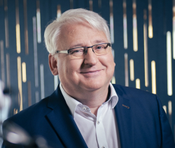
Guy Davies

Guy Davies
Director Business Development Global
DAS En­vi­ron­men­tal Ex­pert GmbH

Guy Davies

Abstract
The semiconductor industry has made a rather mixed response to the carbon neutral requirements as demanded by our current climate challenges. Semiconductor companies have relative conservatively committed to carbon neutrality by 2050 while others have been much more aggressive in their timelines. The subfab and its associated equipment has a considerable impact on the overall eCO2 emissions. This short presentation will discuss the opportunities, potentials and challenges to a carbon neutral footprint particularly focusing on the abatement requirements in the subfab and the interactions with the surrounding equipment.

Biography
Dr. Guy Davies Director Business Development GlobalDr. Guy Davies is Director Business Development Global and member of the management board of DAS Environmental Expert GmbH. He joined DAS in 2011 and since then is focussed on the company’s strategies for product development, innovation management and internationalisation.Prior to his employment with DAS he had 6 years experience working in Semiconductor Manufacturing at Qimonda. Between 1994 and 2003 he worked for ASML, a leading semiconductor equipment manufacturer in a variety of roles worldwide including Research and Development, Customer Support and Strategic Marketing. He completed his Doctorate in optical metrology in 1995 at the University of Edinburgh, a Masters degree at the University of Durham in 1990 and his undergraduate degree in Applied Physics and Electronics in 1989 at Lancaster University.

12:05 Lunch break
12:55 Welcome back
13:00
The environmental footprint of Si chip manufacturing
  Cedric Rolin, Program Manager, Imec
The environmental footprint of Si chip manufacturing
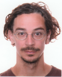
Cedric Rolin

Cedric Rolin
Program Manager
Imec

Cedric Rolin

Abstract
The climate crisis calls for urgent actions towards sustainability as an integral component of businesses and regulations. With its large and growing environmental footprint, the Information and Communication Technology sector is arguably a large part of the problem, but also a part of the solution. Fabrication of integrated circuits is an energy and resource intensive process and the drive towards higher performance and increased functionality increases the process complexity dramatically from node to node. Traditionally, the improvement between technology nodes is evaluated using Power, Performance, Area and Cost (PPAC) metrics in a Design Technology Co-Optimization (DTCO) completely neglecting sustainability. However, this established framework provides an opportunity to do early sustainability assessments of future technologies all the way from material sourcing and fabrication to end of life. To demonstrate this approach, we evaluate the environmental impact, more specifically the energy, ultra-pure water (UPW) and mineral consumption as well as the greenhouse gas (GHG) emissions from manufacturing logic, DRAM and NAND technologies from past to future nodes. Our analysis of logic scaling reveals how the environmental metrics normalized per transistor evolve along with improvements in performance and reduction in cell area.

Biography
Cédric Rolin is Manager for the Sustainable Semiconductor Technologies and Systems (SSTS) Program at imec. He received his M.S. degree and his PhD degree in materials science from the Université Catholique de Louvain in 2004 and 2009 respectively. During the first 13 years of his career (including 2 years postdoc at University of Michigan), Cedric grew his expertise in the thin film growth and manufacturing of devices based on organic semiconductors. Then, from 2018 to 2021, he led a R&D team developing solutions to move flexible thin film circuit and display technologies from the Lab to the Fab. Part of this effort focused on the upscaling of the nanoimprint lithography patterning technology to a 300mm Fab tool. Since November 2021, Cédric has joined the sustainability effort of imec as Program Manager, focusing on the assessment and improvement of the environmental footprint of the semiconductor manufacturing industry.

13:20
Green ICT
  Robert Wieland, Project Manager, Fraunhofer Research Institution for Modular Solid State Technologies EMFT
Green ICT
Robert Wieland

Robert Wieland
Project Manager
Fraunhofer Research Institution for Modular Solid State Technologies EMFT

Robert Wieland

Abstract
Coming Soon

Biography
Coming Soon

13:40 Reserved for business partner
14:00 Panel Discussion
14:30 Coffee break
 

Smart Solutions for Green Manufacturing

14:50 Opening remarks
15:00
Green AI
  John Kelleher, Professor, TU Dublin
Green AI
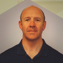
John Kelleher

John Kelleher
Professor
TU Dublin

John Kelleher

Abstract
Coming Soon

Biography
John’s core research expertise is in the areas machine/deep learning and natural language processing. He is the TU Dublin lead in the ADAPT centre and the scientific lead for the Digital Content Transformation Strand. Within the ADAPT centre he leads research projects on language modelling, lexical semantics, machine translation, novelty detection, image captioning, dialog systems, and making AI more environmentally sustainable. John has been the academic lead on numerous industry projects across a range of topics and domains, including: anomaly detection, transfer learning, customer segmentation and propensity modelling, dialog systems and chat bots, and information retrieval and natural language processing.

15:20
Green ICT
  Nils Nissen, Head of Department, Fraunhofer Institute for Reliability and Microintegration IZM
Green ICT

Nils Nissen
Head of Department
Fraunhofer Institute for Reliability and Microintegration IZM

Nils Nissen

Abstract
Coming Soon

Biography
Coming Soon

15:40 Reserved for Flexciton
16:00 Reserved for business partner
16:20
Sustainability Improvements in Semiconductor Manufacturing Using Smart Manufacturing Technologies
  Andreas Neuber, Director Environmental Services, Applied Materials
Sustainability Improvements in Semiconductor Manufacturing Using Smart Manufacturing Technologies
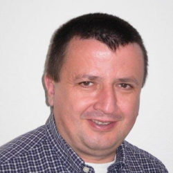
Andreas Neuber

Andreas Neuber
Director Environmental Services
Applied Materials

Andreas Neuber

Abstract
Coming Soon

Biography
Andreas Neuber, Ph.D. has been a Senior Director at Applied Materials since 2008. He has published 80+ papers related to semiconductor fab and facility design, sustainable design and energy savings, water management and recycling, contamination control, and industrial engineering.Prior to joining Applied Materials, Andreas Neuber was Vice President for M+W Zander. During his 18 years at M+W Zander, was involved in semiconductor fab construction and operation/optimization in many locations.Andreas Neuber received a PhD degree in Chemical Engineering from University of Technology Dresden. He is co-chair of the SEMI ESEC task force and the IRDS EHS/S Energy and water reduction roadmap.

16:40
Treading lightly: How a pandemic pivot to remote integrations helped reduce our carbon footprint
  Doug Suerich, Product Evangelist, PEER Group
Treading lightly: How a pandemic pivot to remote integrations helped reduce our carbon footprint
Doug Suerich

Doug Suerich
Product Evangelist
PEER Group

Doug Suerich

Abstract
When the pandemic hit its disruptive peak in 2020-21, the airline industry took a record-breaking tumble as countries restricted travel to limit the spread of COVID-19. For PEER Group, a company that supplies automation software to semiconductor OEMs and factories around the world and relies on onsite discovery, integration, and inspection to deliver and maintain its products, the limitation on international travel forced an immediate pivot to alternative ways of performing these critical functions.As the business world moved to remote work and virtual communication platforms to stay connected with colleagues and customers, so too did PEER Group’s integration and services team to ensure clients and partners continued to receive the same high level of service they were accustomed to pre-pandemic.In this presentation, we’ll share lessons learned from two years of performing remote discoveries, integrations, and inspections and how, in some instances, these lessons have become best practices for our customers going forward. We’ll show how pivoting specific functions to remote platforms has decreased our reliance on air travel, reducing PEER Group’s carbon footprint during the pandemic and, as we continue to improve and develop our remote capabilities, into the future.

Biography
Doug Suerich, Director of Marketing & Product Evangelist, PEER GroupDoug combines more than 20 years of experience creating manufacturing software with a deep desire to help customers find the best solutions to solve their biggest challenges. A passionate advocate for smart manufacturing, Doug is an active member of the SEMI SMART Manufacturing Technology Community, Americas Chapter, and co-chairs the Advanced Process Control Smart Manufacturing Conference.

17:00
Effect of Gas Abatement Selection and Destruction Efficiency on Carbon Neutrality Goals
  Adam Stover, Chief Technology Officer, centrotherm Clean Solutions
Effect of Gas Abatement Selection and Destruction Efficiency on Carbon Neutrality Goals
Adam Stover

Adam Stover
Chief Technology Officer
centrotherm Clean Solutions

Adam Stover

Abstract
Process gas abatement is the backbone of any fab's environmental stewardship program. Proper abatement minimizes not only toxic and hazardous gas release to the environment, but also particulate matter and waste water. Increasingly, gas abatement is measured against its carbon footprint for the input power source, be it electrical or fuel. There is currently a push to go for "carbon free" abatement, using either hydrogen as the fuel gas or electrical systems powered by renewable energy. This goal is indeed laudable, however any carbon footprint calculation should also include the input fuel gas destruction, as they can have extremely high global warming potentials, far above and beyond the input electricity or methane.To that end, this paper makes a full comparison of the carbon footprint for various abatement technologies, taking into account various process gas destruction efficiencies to determine if the power carbon footprint outweighs the non-abated process gases. Additional analyses for regional power generation carbon footprint are also performed.

Biography
Dr. Stover is currently the Chief Technology Officer for centrotherm Clean Solutions USA, based in Albany NY. After completing his bachelors degree in chemistry from Haverford College and PhD from The Johns Hopkins University, he has spent the last 8 years in the semiconductor industry, focused on abatement and achieving sustainability goals.