Friday, November 18, 2022
 

Innovation Showcase

10:00
Time to Collaborate. SubFAB Research and Development
  Ilya Zabelinsky, Co-Founder, ISRL
Time to Collaborate. SubFAB Research and Development
Ilya Zabelinsky

Ilya Zabelinsky
Co-Founder
ISRL

Ilya Zabelinsky

Abstract
The ChallengeThe Semiconductor Industry’s desire for sustainable manufacturing has many challenges to overcome before environmental targets set by most companies can be trustfully met with meaningful positive impact on Global climate changes.One of the key areas poised to become a showstopper for the industry’s ability to achieve sustainability goals is commonly called SubFAB. The SubFAB is a variety of equipment and technologies designed to handle process materials from tool chambers to the factory’s exhaust stacks.Existing infrastructure and siloed approach for SubFAB equipment and technologies R&D can’t support true game changing development of environmentally friendly and affordable solutions to match the manufacturing technologies advancement cadence.This sector is traditionally underserved by fundamental academic research and typically fails to compete for Fab equipment downtime, especially these days when chips shortage keeps factories fully loaded.Chipmakers are forced to spend more capital money on manufacturing capacity and face skyrocketing operational costs. Equipment manufacturers are struggling to meet customer requirements for equipment uptime and Hazadous Air Polutant (HAP) emissions. At the same time academic institutes aren’t involved in research of chemistry and physical nature of post-process material handling.The OpportunityInternational SubFAB Research Labs (ISRL) strategic initiative is being formed these days to pull in an industry-wide collaborative effort on a mission to Bring the Science to SubFAB” and supplement Semiconductor manufacturing technologies advancement with focused research of unwanted and harmful side effects caused by unreacted process materials downstream from process chambers.Member companies will gain access to dedicated facility with complete infrastructure required to operate a set of 300mm process tools with versatile setup of deposition and dry etching process chambers at HVM-like conditions to supplement research and development projects.ISRL will provide its partners a unique opportunity to participate in fundamental research and gain access to common IP or alternatively invest in development of company specific solutions with compartmentalized IP.ISRL will have highly skilled project teams to lead scientific research focusing on reliability issues, technology validation, pathfinding, materials handling and reclaim. Facilities setup will enhance practical skills acquisition for workforce development.

Biography
Ilya Zabelinsky is a globally recognized Technical Leader with over 25 years of experience in vacuum and gas abatement applications for Semiconductor manufacturing.Ilya joined Intel in 1996 to take part in startup and commissioning team of first 200mm fab in Israel, moving on to develop his career as operational and technical leader through several technology node transitions and manufacturing capacity expansion projects. In 2006 Ilya spearheaded an effort to install and commission a full set of vacuum and gas abatement systems for a greenfield construction of 300mm Fab in Kiryat Gat, extending his operational and technical leadership to entire SubFAB ecosystem supporting technology transitions and capacity expansion projects from 45 to 10nm.In April 2022 Ilya left Intel on a mission to “bring the Science to SubFAB” by supplementing Semiconductor manufacturing technologies advancement with focused research of unwanted and harmful side effects caused by unreacted process materials downstream from process chambers.In May 2022 Ilya co-founded International SubFAB Research Labs (ISRL).Ilya possesses broad knowledge and vast practical experience in wide range of semiconductor manufacturing processes, FAB equipment, central facilities systems and infrastructure, spanning from scope definition, programming and design through construction, commissioning and operations. Ilya holds a B.Sc in Chemical Engineering from SCE, Israel. Ilya is passionate practitioner of various education and mentoring programs aimed at new generations of professional and diverse workforce.

10:15
Keep It Simple & Save (KISS) in Burn-In Operations
  Joe Tan, Founder & Managing Director, MSV Systems & Services Pte Ltd
Keep It Simple & Save (KISS) in Burn-In Operations
Joe Tan

Joe Tan
Founder & Managing Director
MSV Systems & Services Pte Ltd

Joe Tan

Abstract
Typical semiconductor burn-in operations have multiple burn-in systems, auto-loaders & a huge quantity of burn-in boards on racks or trolleys.Limited integration between equipment had resulted in significant manual handling activities, which in turns had caused low OEE, high maintenance & high resource wastages.While many companies had attempted to automate the burn-in operations through the use of robotics & AMR, the cost of both implementation & maintenance is prohibitive. Moreover, there are little efficiency gain with these attempts & operational flexibility can be significantly compromised.This presentation showcase how a small change in the burn-in chamber design based on our patented MudaX solution, can help companies Keep It Simple, solves most, if not all the operational challenges in burn-in & Saves significant cost in burn-in operations.This presentation has very recently won the Most Inspirational Presentation award in TestConX USA conference in Arizona in May 2022.

Biography
Joe Tan is the Founder & Managing Director of MSV Systems & Services Pte Ltd established in Singapore in 2002.He graduated from the National University of Singapore with a Honours Degree in Electronics Engineering & a Master’s Degree in Industrial & System Engineering.After over 20 years of providing technical service on burn-in systems, auto-loaders & burn-in boards. MSV had invested in R&D & patented the MudaX solution to help companies Keep It Simple & Save (KISS) in burn-in operations.

10:30
Intelligent wafering: how to widen the bottleneck in semiconductor substrate manufacturing
  Ivan Orlov, CEO, Scientific Visual S.A.
Intelligent wafering: how to widen the bottleneck in semiconductor substrate manufacturing
Ivan Orlov

Ivan Orlov
CEO
Scientific Visual S.A.

Ivan Orlov

Abstract
Impacted by the COVID19 pandemic and the war in Ukraine, the semiconductor market experiences unprecedented shortages. The primary bottleneck is the wafer production, which is costly and resource-intensive. As an aggravating factor, its yield is not very high: the bulk crystalline material intended for wafering is usually inspected with the human eye so that internal defects present in the ingot often end up in the finished wafers and cause their rejection. In this study, we show how to increase the wafering yield by computer-aided optimization of the wafering positions, an “intelligent wafering” method.In a typical production, semiconductor cores are extracted from an ingot with an irregular 3D shape and later sliced into wafers with a regular grid of wires. Industrial applications require wafers of standard diameters, thicknesses, and orientation, that set characteristics of the core.When internal defects are present in the core, their positioning to the cutting planes matters. Knowing the precise defect coordinates and dimensions allows calculating a core position that fits more defects into sawing gaps and, therefore, out of future wafers.We developed an “intelligent wafering” routine that computes the most optimal core position in a wafering system. It is based on digital crystal twins obtained with a TotalScan™ scanner from raw crystals. The scanner automatically detects bubbles, structures, and clouds down to 10 μm in raw crystals ranging from 0.3 kg to 350 kg. The corresponding 3D defect patterns are then analyzed using the Yield Pro v4.4 software to derive the optimal offset of the wafering grid.The method consists of the following steps:1. Scan a crystal to obtain its 3D digital twin, including internal defect morphology and spatial coordinates.2. Add orientation of crystal axis to the digital twin.3. Optimize coring positions within the crystal volume with a defined angle to a crystal axis.4. For each core, based on its defect pattern, compute an offset of the slicing grid towards the core reference that positions most of the core defects into sawing gaps.5. Adjust the position of the slicing wires to the core according to the computed offset.We will show practical examples of how intelligent wafering gets up to 7% more non-defective wafers than “blind” wafering used today. It confirms that the digitalization of crystal quality control offers tangible opportunities for processing companies to extract more quality wafers and save resources.

Biography
Dr. Ivan Orlov earned a PhD in Crystallography in Switzerland. His career embraces 20 years of R&D experience on non-destructive quality control technologies applied to optical materials and industrial crystals. He was a member of the SEMI Task Force for sapphire standard in China and collaborated with the ISO committee to establish the sapphire quality certification. Since 2010, he is leading Scientific Visual, a Swiss corporation supplying solutions for quality control of synthetic crystals.

10:45
New Metrology Technique for Measuring Patterned Wafer Geometry on a full 300mm wafer
  Jan Gaudestad, VP Business Development, Wooptix
New Metrology Technique for Measuring Patterned Wafer Geometry on a full 300mm wafer
Jan Gaudestad

Jan Gaudestad
VP Business Development
Wooptix

Jan Gaudestad

Abstract
The flatness of the silicon wafers used to manufacture integrated circuits (IC) is controlled to tight tolerances to help ensure that the full wafer is sufficiently flat for lithographic processing. Chemical-Mechanical Planarization (CMP) is one of many processes outside the lithographic sector that will influence wafer flatness across each image lithographic exposure section field and across the wafer. Advanced lithographic patterning processes require a detailed map of the wafer shape to avoid overlay errors caused by depth-of-focus issues. In recent years, a metrology tool named PWG5TM (Patterned Wafer Geometry, 5th generation), based on using double Fizeau interferometry to generate phase changes from the interferometric pattern applied to the reflective surface, has been used to generate a wafer geometry map to correct for process induced focus issues as well as overlay problems. In this paper we present Wave Front Phase Imaging (WFPI); a new patterned wafer geometry technique that measures the wave front phase utilizing two intensity images of the light reflected off the patterned wafer. We show that the 300mm machine acquires 7.65 million data points in 5 seconds on the full 300mm patterned wafer with a lateral resolution of 96µm. For the semiconductor industry to uphold Moore’s Law, among the key challenges are the ever-tightening overlay requirements. In the latest immersion scanners that perform at the sub-2 nm overlay level, the overlay budget becomes more and more determined by process-induced overlay errors from fab steps such as etching, thin film deposition, Chemical-Mechanical Planarization (CMP) and thermal anneal. All these processing steps can introduce stress, or stress changes, in the thin films on top of the silicon wafers that again can result in significant wafer distortions. Since the data acquisition time of Wave Front Phase Imaging (WPFI) is mainly controlled by the shutter speed of the camera when used in a dual camera set up, which is generally set to less than a second, in addition to very high data count, it makes WPFI a strong alternative technique for measuring and correcting for process induced stress quickly. Adding that WFPI is highly resistant to vibrations in addition to having large tolerances to wafer placements in the optical measurement cavity, makes WFPI a viable solution in a high-volume device manufacturing fab setting.

Biography
Jan Gaudestad is San Francisco based VP of Business Development for Wooptix, a small VC funded Intel Capital portfolio company, that is developing metrology equipment for the semiconductor fab market. He also serves on the board of directors for Elevate Semiconductors, a fables semiconductor company based in San Diego California. He has more than 20 years of experience in the semiconductor industry. He worked on strategic accounts at InvenSense/TDK for consumer level MEMS motion sensors. He spent 14 years at Neocera, an Intel Capital funded backend semiconductor equipment company managing product development, global sales, applications, and new business development. He also spent time working on emerging technologies for virtual and augmented reality applications. He received his MBA from Santa Clara University in 2009. He earned a master’s degree in Physics in 2001 from University of Maryland, College Park, and a master’s degree in Physics in 2000 from the Norwegian University of Science and Technology in Trondheim, Norway.

11:00
Minimizing Execution Risk in Test Solution Development Projects with a Technical Project Lead
  David Ducrocq, Application Test Technical Leader, TERADYNE
Minimizing Execution Risk in Test Solution Development Projects with a Technical Project Lead
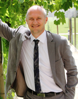
David Ducrocq

David Ducrocq
Application Test Technical Leader
TERADYNE

David Ducrocq

Abstract
Test development projects are a mix of engineering disciplines spanning PCB design and layout, software engineering, measurement technology, test system configuration and test cell setup, a complex and interdependent ecosystem. A project manager, who is primarily focused on schedule, is unable to oversee the many disciplines and adequately assess technical risks in each area and across the entire project. This inability to assess risks and their impact on the entire project is often the root cause of catastrophic project failures and missed delivery schedules. By including a technical project lead in the project, there is a single point of responsibility for assessing technical risk across the project, developing mitigation plans and driving countermeasures to completion.This paper will address:1. The role the technical project lead plays with each stakeholder in the project and to the project as a whole, including:1.1 solution architecture1.2 resource identification and allocation1.3 technical execution of the project1.4 issue mitigation and resolution1.5 communications with both internal and external stakeholders2. Qualifications of a technical project lead3. An overview of the risk assessment and mitigation process4. Expected benefits to the project, team and working environment

Biography
David Ducrocq is an Application Project Leader at Teradyne, where he focuses on PMIC and Image Sensor Test program development and is a specialist on Teradyne’s FLEX, MicroFLEX and UltraFLEX test systems. David has played a leading role in defining and implementing Teradyne’s technical project lead program across the organization. David joined Teradyne in 1999 as an Applications Engineer for the Test Assistance Group in Grenoble/France, where he worked on Catalyst on RF Devices.David studied Electrical Engineering and Computer Science at the Institute de Recherche et d'Enseignement Superieur aux Techniques de l'Electronique* (IRESTE), Université´ de Nantes, France.After graduation, David worked in the field of Image Processing for 2 years. He then worked as a subcontractor for Teradyne for 4 years on the A3xx, A5xx and Catalyst test systems.In 1999, David joined the Test Assistance Group at Teradyne in Grenoble/France as an Applications Engineer. David worked on Catalyst on RF Devices and is now a specialist on FLEX/MicroFlex/UltraFlex test systems.From 2012, David took the responsibility of several key customers as an Application Project Leader mainly focusing on PMIC and Image Sensor Test program development. During this period, David played a leading role in definition and implementation of the technical project lead and was in charge of its roll-out throughout the corporation.*Institute of Research and Higher Education for the Techniques of Electronics

11:15
Wafer contamination detection: an unsupervised learning approach
  Reza Hajiahmadi, Data scientist, ASML
Wafer contamination detection: an unsupervised learning approach

Reza Hajiahmadi

Reza Hajiahmadi
Data scientist
ASML

Reza Hajiahmadi

Abstract
The wafer particle contamination (backside and frontside) inside semiconductors factories is often very late detected in the production process and the impact of that is significant, as it can introduce yield loss and large down time on the litho tools.Unfortunately, there is no easy-to-use monitoring tool to detect, quantify and classify all forms of particle contamination on the wafer. We have developed a solution based on the open-source data science KNIME Analytics platform, in which we have used signal processing and machine learning techniques to detect, quantify and classify the contaminated areas using wafer height data. To be more specific, our solution is able to fully detect backside particles clamped between the wafer and the wafer table burls. And as for the frontside particle, our tool is able to detect the ones that are larger than 10nm in height and 3.3 um in area.The prototype we developed contains a dashboard deployed in a web browser on the lithography tools and can easily be used real-time by customers in their fabs. The users can easily monitor wafer contamination and the health of the wafer table instantly and through time without the need to store large amount of data and/or installing tools on local computers.The proposed solution is able to automatically detect any number of clusters of bad spots in a wafer map. The solution consists of wafer’s height data units, spot detection, spot classification and KPI reporting and visualization. In more detail:Slope detection mechanism of bad spots instead of plain wafer observation and a new fully automated algorithm (DBSCAN, a density based algorithm that does not need prior training nor the number of groups/clusters that they data contains) to classify the detected spots. The classified spots/shapes help the operator find the root causes of the contamination.Reporting (in the form of an inline monitoring dashboard deployed on the litho tool) the statistics and the characteristics (shape, hint on root cause, etc.) of the identified clusters of contamination particles to the users and notifying the operator if the level of contamination exceeds a defined threshold.Identification of persistent spots (wafer heatmap) on multiple wafers that could provide insight on whether the contamination is caused by wafer table damage, backside features and/or other process related issues in the fab.­­

Biography
Reza Hajiahmadi obtained his PhD, cum laude, in Applied Mathematics from Delft University of Technology in 2015. He has been working at ASML as a data scientist and senior lithography engineer for 6 years and has published several patents and publications as part of his research in metrology, lithography and field data mining techniques.

11:30
Spectral Interferometry (SI) And Vertical Traveling Scatterometry (VTS) Technology For Advanced Metrology Of Back-End-Of-Line (BEOL) Manufacturing Process Steps
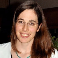
  Dana Szafranek, Algorithm scientist, Nova Ltd
Spectral Interferometry (SI) And Vertical Traveling Scatterometry (VTS) Technology For Advanced Metrology Of Back-End-Of-Line (BEOL) Manufacturing Process Steps
Dana Szafranek

Dana Szafranek
Algorithm scientist
Nova Ltd

Dana Szafranek

Abstract
We present advances in optical critical dimension (OCD) metrology for back-end-of-line (BEOL) manufacturing process steps. Semiconductor device fabrication has advanced rapidly in recent decades, in part due to OCD metrology. Standard techniques for OCD are either spectral reflectometry and/or ellipsometry (SR/SE). We present here a new technology – Spectral Interferometry (SI)- implemented on the Nova PRISM OCD platform as a unique capability in Nova’s high-end Stand-Alone metrology solution portfolio. SI extracts unique spectral information from the sample, inaccessible by current technologies. To complement Nova PRISM, the SI data is processed with a novel algorithmic suite called Vertical Travelling Scatterometry (VTS). VTS enables selective OCD analyses of the top part of a sample separately from the bottom part of a sample within a single metrology step. Thus, it is possible to focus selectively on the topmost layers of interest to simplify the complexity of traditional OCD modeling. Multiple benefits include enhanced robustness by controlling metrology consistency under incoming variations, reduced time-to-solution due to the simplified geometry, and feasibility of modeling complex in-die applications. Recent developments in the fabrication of logic circuits and memory elements require advanced dimensional metrology steps very late in the semiconductor production process, e.g., in the back-end-of-line (BEOL) process steps where it was previously not required. Moreover, the varied topology of the samples renders metrology of the fully integrated device, i.e., metrology “in-die”, preferable, rather than using a dedicated metrology target in the scribe line. However, an “in-die” sample with many layers and buried three-dimensional architectures introduces many degrees of freedom to traditional OCD that represent the cumulative possible process variations. As a result, traditional OCD approaches based on scatterometry may not be capable of the required precision for tight process control of the BEOL process steps. It is especially beneficial to apply SI and VTS for such BEOL applications, since the separation of “relevant” and “irrelevant” information correlates to the depth of the optical signal, and thus simplifying the resulting geometric die model.

Biography
Dr. Szafranek is an algorithm developer within the semiconductor industry. Earlier in her career, she focused on computational methods for electromagnetics. In recent years, Szafranek took part in projects involving machine learning, data augmentation, feature extraction, etc., while always keeping herself minded towards the underlying fundamental physics and full physical modeling.

12:00
Technology that makes Technology Sustainable
  Claire HyunJung Seo, Corporate Vice President DS Corporate Sustainability Management Office, Samsung Electronics
Technology that makes Technology Sustainable
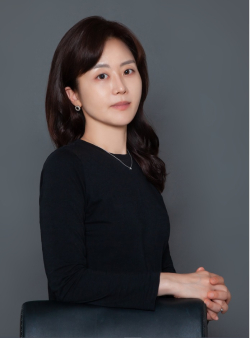
Claire HyunJung Seo

Claire HyunJung Seo
Corporate Vice President DS Corporate Sustainability Management Office
Samsung Electronics

Claire HyunJung Seo

Abstract
Semiconductor continues to develop innovative core technologies and responsibly address the challenges we face in our environment today. It is through technology, we strive to minimize our impact on nature. As industry’s global leader, we communicate with our stakeholders across the supply chain to build an eco-friendly value chain. From sustainable productions to providing low power technologies, Samsung Semiconductor actively participates and creates standards for our industry to act under one purpose. At Smart and Green Manufacturing Summit we share our eco-conscious efforts thus far as well as our environmental goals toward a sustainable future.

Biography
Claire HyunJung Seo, is Corporate Vice President at Samsung Electronics DS Division, Corporate Sustainability Management Office and leads corporate sustainability and ESG integration for the Division.Claire’s expertise is in responsible investment and sustainability consulting and brings more than 20 years of experience from the field, mainly based in Asia and US.