Thursday, November 17, 2022
 

SCREEN: Innovation Inspired By Sustainability

09:45 Welcome Note, Dr. Martin Hollfelder, Director of Technology and Service, Europe
09:50

Keynote

 
Sustainability Driven Innovation: transistor scaling and defectivity targets for sustainable manufacturing
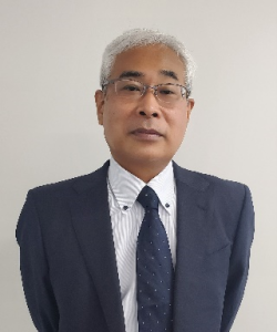
  Okuno Yasutoshi, Vice President & Corporate Officer of Technology Strategy, SCREEN Semiconductor Solutions Co.
Sustainability Driven Innovation: transistor scaling and defectivity targets for sustainable manufacturing
Okuno Yasutoshi

Okuno Yasutoshi
Vice President & Corporate Officer of Technology Strategy
SCREEN Semiconductor Solutions Co.

Okuno Yasutoshi

Abstract
A key requirement for sustainable innovation is achieving the highest number of good known die (KGD) per wafer. Historically, this has been achieved in parallel with the introduction of larger wafers (greater area), minimizing die size with transistor two-dimensional (2-D) scaling, and improving die quality with defect reduction and yield enhancement efforts.As wafer size has reached a plateau at 300mm - transistor scaling has transitioned from 2-D to 3-D technologies. 3-D scaling, supported by disruptive technologies such as FinFet, Nanosheet, and Forksheet, will reach an end by 2030. The ultimate frontier of transistor scaling relies now on the complementary FET (CFET) approach, which will unlock the Z-dimension scaling.Z-dimension scaling will face significant challenges to achieve both high yield and reduce the ecological footprint of the manufacturing process and supply chain. To achieve the targets, sophisticated techniques for early defect detection, quantification, and removal will need to adopt.Reaching carbon neutrality is a collective effort, and the operational perspective, including new materials introduction, fab management, and manufacturing equipment design - including the whole supply chain – is an important part of the equation.In this presentation, we explore the scaling roadmap for logic devices, requirements for layer-based tolerable defects with growing device complexity and show examples of technology solutions to achieve high yield with a lower ecological footprint reduction.

Biography
Dr. Yasutoshi Okuno received a Ph.D. degree in engineering from Osaka University, Osaka, Japan, in 1993. He is currently serving as Vice President & Corporate Officer of the technology strategy at SCREEN Semiconductor Solutions Co., Ltd. since 2021 and has been responsible for the technology strategy since 2010. Before that, he managed a module process team for advanced CMOS pathfinding at TSMC for 9 years. His carrier in the field started at R&D Group, Texas Instruments, Inc., Tsukuba, Japan, and moved to Memory R&D Group, Kilby Center, Texas Instruments, Inc. as a FEOL Process Engineer. In late 1998, he is with the ULSI Process Development Group, Panasonic Corporation, where he led the FEOL module integration for the advanced CMOS process.

10:10
Exotic applications of nanosecond laser annealing
  Sébastien Kerdilès, Head of Thermal Treatments Engineering, CEA – LETI
Exotic applications of nanosecond laser annealing
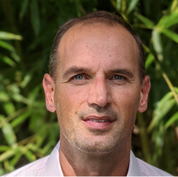
Sébastien Kerdilès

Sébastien Kerdilès
Head of Thermal Treatments Engineering
CEA – LETI

Sébastien Kerdilès

Abstract
The need for lower and lower thermal budget in microelectronics has driven annealing technologies from furnaces to millisecond processes. The era of nanosecond laser annealing (NLA) is coming. On one hand, such technique enables treatments at very high temperatures in the melt and sub-melt regimes, with unprecedented cooling rates, that give access to very high active dopant concentrations. One the other hand, thanks to its short pulse duration, NLA also enables surface heating with an excellent in-depth selectivity, which is particularly suited for various 3D architectures. In this presentation, several More-than-Moore applications of NLA currently developed at CEA-LETI will be shared. The use of NLA will be illustrated for 3D sequential integration, for ferroelectric memories integrated in the BEOL and for exotic applications leveraging superconducting silicon.

Biography
Dr. Sébastien Kerdilès received a Ph.D. degree in materials science from the University of Caen, France, in 2000. Then, he worked for 2 years for a start-up in the Paris area. From 2002 to 2013, he worked for SOITEC as a research staff member first, then as a technology development manager, and finally as an SOI designer. During this period, he contributed to the industrialization of 200 & 300mm SOI substrates manufacturing, including RF-SOI and Fully depleted SOI. In 2013, he joined CEA-LETI, where he is in charge of thermal treatments. His research interests include the investigation of pulsed laser annealing for various applications such as 3D integration, memories, and MEMS. He authored or co-authored more than 50 journal articles and conference papers and holds over 20 patents.

10:30
Sustainable SiC: the Advantages of Engineering Substrates
  Nicolas Daval, Expertise Labs Senior Manager, Soitec
Sustainable SiC: the Advantages of Engineering Substrates
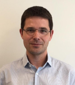
Nicolas Daval

Nicolas Daval
Expertise Labs Senior Manager
Soitec

Nicolas Daval

Abstract
Engineering substrates are an effective way to bring additional functionalities and more performance to electronic applications. The substrate is seen as a stack where each layer is optimized for its function. Smart Cut greatly expands the possibilities since it enables a perfect crystalline layer to be put on top of any material, regardless of its crystal structure.Applying this concept to SiC power device, the SiC engineering substrate should have a top layer to be a template for SiC drift epitaxy growth, the bulk of the substrate should provide very low resistance to the vertical current flow, the wafer geometry should remain compliant with device processing requirements throughout the device processing. Finally, there is an opportunity to provide a substrate with an overall carbon emission largely reduced compared to the reference SiC bulk material.This talk will describe SmartSiC, the SiC-engineered substrate, which includes all the elements listed above.

Biography
Dr. Nicolas Daval received his Master of Science from Ecole supérieure de Chimie Physique Electronique and his PhD from Institute National des Sciences Appliquées in Lyon. He started as a Ph.D. student already at SOITEC and he was holding various positions as R&D Engineer, and Project Manager. Today he is Expertise Labs Sr Manager at SOITEC in the innovation department, leading process evolution based on physics understanding and modelization.

10:50
Towards Sustainable Wet Processing for Advanced Integration Technologies
  Dr. Efrain Altamirano-Sanchez, R&D Manager of SIP group, imec
Towards Sustainable Wet Processing for Advanced Integration Technologies
Dr. Efrain Altamirano-Sanchez

Dr. Efrain Altamirano-Sanchez
R&D Manager of SIP group
imec

Dr. Efrain Altamirano-Sanchez

Abstract
The new challenges for wet processing are associated with the new materials and the scaling roadmap for Logic, Memory, and 3D system integration (STCO) i.e CFET, 3D Memory, D2W, W2W, and FOWLP. The specifications for defects, pattern-collapse, selectivity, and uniformity will be tighter and tighter, demanding more advanced hardware and formulated chemicals. One challenge for the cleaning community will be how to contribute to maximizing the wet processing performance and the cost-benefit. In the Semiconductor industry, wet processes are more and more critical but also resources intensive in energy, water, and chemicals. Hence, another big challenge ahead for the cleaning community is how to minimize GHG emissions and abide by the announced targets for net-zero carbon emissions by 2050. In this paper, examples of the above-mentioned technologies and the related wet processes will be discussed.

Biography
Dr. Efraín Altamirano-Sánchez holds a Ph.D. in Chemical Engineering. He joined imec in 2006 where he developed strong expertise in advanced patterning for technologies nodes ranging from 65 nm to 5 nm. In 2018, he joined the wet processing team as a group manager. He is now focused on the innovation of wet process solutions for CFET, 3D DRAM, 3D integration & sustainability.

11:10
How can Track Hardware Boost Lithographic Performance?
  Andreia Santos, R&D Manager, SCREEN Semiconductor Solutions Co.
How can Track Hardware Boost Lithographic Performance?
Andreia Santos

Andreia Santos
R&D Manager
SCREEN Semiconductor Solutions Co.

Andreia Santos

Abstract
To keep up with the technology roadmap evolution, lithography track performance capabilities have also rapidly expanded through the years and new modules are being specially designed to support resist suppliers achieve the stringent patterning requirements currently in place.In this work, we showcase the capability of novel hardware solutions currently available on SCREEN’s DT-3000 coat-develop track system to improve EUV process stability and defect performance. Based on a holistic approach, we demonstrate how hardware development is still a key not only to improving process stability and driving down defectivity to unprecedented low levels, but also to boosting other metrics such as line width roughness (LWR), defect-free process window, and pattern shape.

Biography
Andreia Santos received 2008 her master’s degree in chemical engineering from Aveiro University in Portugal, where she focused on polymer chemistry and material characterization. Her first experience in the semiconductors world was in 2011 when she joined Nanium - a wafer-level packaging company - as a photolithography process engineer. Two years later, she moved to Belgium to start working at JSR Micro – a leading materials supplier - where she had the opportunity to get a deeper understanding of photoresist chemistry. After working for a chip maker and a resist supplier, in 2020 Andreia decided to join Screen’s team at Imec, where she currently works as an R&D Manager.

11:20
Reducing Bulk Chemicals by SPM Reuse in Single-Wafer Process Applications
  Jim Snow, Senior Technologist, SCREEN SPE USA
Reducing Bulk Chemicals by SPM Reuse in Single-Wafer Process Applications
Jim Snow

Jim Snow
Senior Technologist
SCREEN SPE USA

Jim Snow

Abstract
High-purity sulfuric acid (H2SO4) is used as a mixture with hydrogen peroxide (H2O2), i.e., SPM, sulfuric peroxide mixture, or “piranha etch”, in the semiconductor industry for the oxidative decomposition and removal of organic materials, e.g. photoresist, and residues, e.g. from post plasma strip, from silicon wafers. Sulfuric acid is one of the most widely used chemicals in the microelectronics industry and the continuing increase in the number of processing steps and demand for electronic devices worldwide is expected to increase the annual consumption of sulfuric acid. The global electronic-grade sulfuric acid market size was assessed to be $305M in 2021 and is projected to reach $415M by 2026. (1) The quantity of SPM and required rinsing chemicals on the environment, safety, and health (ESH) represents a serious drawback. To help reduce the environmental impact of sulfuric acid and actively contribute to our customers’ environmental preservation efforts, SCREEN Semiconductor Solutions has developed an SPM reclaim function on their single-wafer SU-3300 platform. (2) The dispense volume of H2SO4 can be reduced significantly with equivalent process performance. In addition, the potential replacement of SPM with another chemistry will be presented.

Biography
Dr. Jim Snow is a Senior Technologist at SCREEN SPE USA, where he currently manages JDP activities and sustainability efforts. Prior to joining SCREEN, he was a Group Leader in the Ultra Clean Processing group at IMEC and began his career in the semiconductor industry at Millipore Corp (now Entegris). He received his Ph.D. in chemistry from MIT. Dr. Snow has numerous publications in journals, book chapters, patents, and conference presentations.

11:35
High-Volume Automatic Visual Inspection and Trench Thickness Measurement on Si, SiC, and GaN wafers
  Alessandro Rossi, Product Manager and Application Engineer, SCREEN SPE Europe
High-Volume Automatic Visual Inspection and Trench Thickness Measurement on Si, SiC, and GaN wafers
Alessandro Rossi

Alessandro Rossi
Product Manager and Application Engineer
SCREEN SPE Europe

Alessandro Rossi

Abstract
SCREEN offers very competitive and low CoO technical solutions to support 6-inch/8-inch wafers for automotive, power devices, and IoT applications as defects inspection (AVI) and thickness measurement tools.On defectivity inspection tools SCREEN enhanced the current platforms, ZI-2000 and ZI-3500 with the availability of a new high throughput, the upcoming new inspection tool which is capable to double the number of inspected wafers and it has sub-micron defects detection capability, responding on strong market demand, providing a faster return of the investment and flexibility. It can also handle up to 12-inch wafers.On the thickness measurement tools portfolio, which is based on a spectroscopic reflectometer or ellipsometer, we investigate new trench depth measurements with mask film thickness separation application.

Biography
Alessandro has an Electrical engineering degree in Electronics and Electrics Industries. He has been working with Screen for 25 years, covering European customer service, litho application development, and metrology and inspection platform management. He has been involved in Joint Development Projects for immersion lithography and negative tone development.

11:50
Screen UV Laser Anneal Technology
  Louis Thuries, Product Manager, SCREEN LASSE
Screen UV Laser Anneal Technology
Louis Thuries

Louis Thuries
Product Manager
SCREEN LASSE

Louis Thuries

Abstract
Ultimate control of the thermal budget, both in time and in-depth, is made possible by combining surface-selective anneal enabled by UV laser and control of heat diffusion enabled by tuning the irradiation duration in the µs timescale.Such technology opens a new space in between sub-melting standard techniques, such as furnace anneal or flash lamps anneal, and nanosecond melting UV laser anneal.For Si IGBT, UV µs LA allows activation of p/n junction in a diffusion-less single-step process. Thanks to the ultimate control of heat penetration depth, UV µs LA is suitable for all kinds of profiles up to 5 µm while staying compatible with thin wafers.SiC power devices have emerged as a breakthrough technology for a wide range of applications, from inverters for automotive to fast charging stations. Fabricating low-resistance ohmic contact with good reliability and mechanical performances is still challenging, and UV µs LA is shown to lead to uniform and continuous formation of NixSiy films. Finally, crystal curing and dopant activation after ion implantation by laser anneal, in a cost-effective and protective capping-less integration, is a major step forward and opens new routes for SiC power MOSFETs.

Biography
Louis THURIES is the product manager at SCREEN LASSE. Before that, he was based in Taiwan as an application, process, and product development engineer. He extensively worked with R&D centers (LETI/imec/IBM) for application development, focusing on advanced logic, CIS, power, and memory devices. Before LASSE, he was working on GaN HEMT development in Grenoble.