Wednesday, November 16, 2022
 

Materials Innovation

09:50 Opening remarks
  Hessel Sprey, Manager External R&D and Cooperative Programs, ASM Belgium
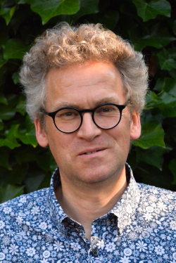
Hessel Sprey

Hessel Sprey
Manager External R&D and Cooperative Programs
ASM Belgium

Biography
Hessel Sprey received his M.Sc. in experimental physics from the University of Leiden (The Netherlands) in 1989, and joined ASM International in 1990.He has been active in equipment and process R&D at various ASM and customer locations for several of ASM’s product lines, since 1996 in project and team leader positions.He has been project and workpackage leader for several European projects, is (co-)author of more than 60 scientific papers and conference contributions on deposition processes, equipment and applications, and holds 22 patents and patent applications.He is currently based in Leuven, Belgium, with as main activity the coordination of ASM's External R&D activities and cooperative programs.

10:00
Semiconductor Market Expansion Driving Materials Innovation – Materials Market Outlook and Challenge
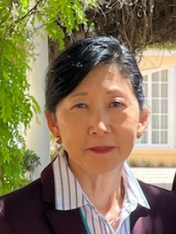
  Lita Shon-Roy, President/CEO and Founder, TECHCET
Semiconductor Market Expansion Driving Materials Innovation – Materials Market Outlook and Challenge
Lita Shon-Roy

Lita Shon-Roy
President/CEO and Founder
TECHCET

Lita Shon-Roy

Abstract
Coming Soon

Biography
Lita Shon-Roy - President/CEO and Founder of TECHCET— has worked throughout the semiconductor supply chain at various levels leading strategy, business development, marketing and sales for chip designers, equipment OEMs, and electronics material suppliers for over 30 years. Her experience spans from process development of SRAMs to business development of gases & precursors. She developed new business opportunities for companies such as RASIRC/Matheson Gases, Air Products & Chemicals, and IPEC/Speedfam, and managed marketing and sales in companies such as Air Products/Schumacher, Brooktree/Rockwell, and Hughes Aircraft. Ms. Shon-Roy is considered one of the leading experts in electronic materials market research analysis and business development. She has authored and co-authored 100’s of articles, reports and texts on semiconductor process materials markets, trends, and worldwide supply chain issues. She holds an M.B.A. from California State University, Dominguez Hills, a M.S.E.E. focused on Solid State Physics from the University of Southern California, and a B.S. in Chemical Engineering from UC San Diego.

10:20
Current Trends in Digital Chemistry to Drive Semiconductor Innovation
  Simon Elliott, Director - Atomic level process simulation, Schrödinger
Current Trends in Digital Chemistry to Drive Semiconductor Innovation

Simon Elliott

Simon Elliott
Director - Atomic level process simulation
Schrödinger

Simon Elliott

Abstract
The semiconductor industry is of course the enabler of digitization, but some commentators have pointed out the irony that it lags behind other industries in its own adoption of digital practices of "Industry 4.0". Looking in particular at R&D, the cost of achieving each successive technology node continues to climb steeply. With the 5 nm node estimated to cost a company $0.5bn in R&D, immense savings could be made through increased digitization of R&D activities. Such changes will be natural for today's workforce of digital natives, who access data on the cloud, share information in social networks and dial in to meetings online regardless of geography.Another aspect of the digital revolution is the transformative effect of easy access to vast computing power, and here too the semiconductor industry can benefit from its own technology. In the ideal situation, hypotheses will be tested first in simulation, as this should be both cheaper and more systematic than lab-based experiments. Looking at materials and process R&D, we discuss whether simulation software has achieved the accuracy, ease-of-use and robustness to allow this. We also focus on how to bridge gaps in expertise. Finally, we consider examples of machine learning in materials R&D and how improvements in data curation are needed right across the R&D landscape.

Biography
Co-author Dr Mathew D. Halls is Senior Vice President, Materials Science, Schrödinger.Presenting author Dr Simon Elliott is Director of atomic level process simulation at scientific software company Schrödinger, where he develops and applies techniques based on quantum mechanics and/or machine learning to the surface chemistry of deposition and etch. Prior to this, he studied chemistry at Trinity College Dublin and Karlsruhe Institute of Technology, and until 2018 led research on modelling atomic layer deposition at Ireland's Tyndall National Institute. He was co-chair of the 16th International Conference on Atomic Layer Deposition and chair of the 175-member European network on the same topic. He can sometimes be found introducing theatre improvisation games to scientists as a route to better communication skills.

10:40
EUV Lithography Patterning: Status and Challenges Towards High NA
  Danilo De Simone, Staff Member, Imec
EUV Lithography Patterning: Status and Challenges Towards High NA
Danilo De Simone

Danilo De Simone
Staff Member
Imec

Danilo De Simone

Abstract
Nowadays, the device scaling driven by the Moore’s law is continuing by the deployment of the 0.33NA extreme ultraviolet lithography (EUVL) in high volume manufacturing for single print and multi-patterning schemes further driven by the need to improve cycle time and cost. To further simplify and improve EUV patterning reducing cost and enable 2nm technology and below, high NA EUV lithography is under development and in 2023 imec and ASML will open a high NA EUV Lab, where the first high 0.55NA scanner will be installed.At the same time, as the nanoscale is pushed further down, the stochastic nature of the patterning process becomes one of the major patterning roadblocks. To enable the high NA technology new knobs and faster learning cycles on patterning process development are needed to improve the process window and minimize the stochastic patterning defectivity issues. Lithography solutions can’t afford alone the stochastic challenges; thus, the etching and thin film processes become essential to holistically offer, together with the lithographic process, novel clean pattering solutions. This presentation will show the latest development on EUV patterning materials and their challenges and provide an insight status of overcoming these obstacles towards high NA.

Biography
Danilo De Simone holds a MS degree in chemistry from the university of Palermo (Italy) and has 22 years of experience in semiconductor R&D field. He led the development of lithographic materials for 90nm and 65nm NOR Flash devices for STMicroelectronics (STM) in Italy and covered the role of assignee at STM Alliance in France and STM in Singapore. In 2008, he joint Numonyx to lead the R&D development for lithographic materials and first 32nm double patterning for PCM devices. In 2011, he moved to Micron Technology to introduce 45nm phase-change-memory devices in HVM, and to develop patterning solutions for novel devices. In 2013, he joined the international nanoelectronics research center imec leading the research on patterning materials for EUV lithography. He is editorial board member of the Journal of Micro/Nanopatterning, Materials, and Metrology (JM3), member of SPIE committee for the Patterning Materials and Processes program and member of the International Advisory Board of the Photopolymer Science and Technology Conference (ICPST).

11:00
Nanoscale Metals are Comprised of Grain Boundaries that are Significantly Different from those found in Bulk Materials

  John Boland, Professor of Chemistry, Trinity College Dublin
Nanoscale Metals are Comprised of Grain Boundaries that are Significantly Different from those found in Bulk Materials
John Boland

John Boland
Professor of Chemistry
Trinity College Dublin

Abstract
Metals are the simplest of solids and copper is probably the best known and most studied of all. The properties of copper metal of macroscopic dimension are well understood. However, the same cannot said when copper is reduced to nanoscale dimensions. Like most metals, copper is a granular solid comprised of grains with boundaries between them. Here in this talk we focus on what we have learned about nanoscale copper by using scanning tunneling microscopy and molecular static simulations. In particular we visualize for the first time the 3D structure of grain boundaries (GBs) that emerge at the surface of nearly coplanar copper nanocrystalline (111) films. Remarkably, we find that GBs at surfaces are different from those in the bulk. We show that GBs in metals actually prefer to lie along close packed planes which in turn necessitates the tilting and restructuring of the boundary as it approaches the (111) surface. The restructuring depth can be a few to several tens of nanometers. This behavior is due to a previously unrecognized phenomenon that involves the rotation of the dislocation lines that comprise the GB, which minimize the energy and has significant implications for materials properties [1, 2]. Since transport in copper occurs predominantly along close packed planes these restructure boundaries, which also lie along close packed planes, are expected to have unusual scattering properties. Whether fully relaxed restructured boundaries are possible under device fabrication conditions remains to be established.References:[1] Xiaopu Zhang, Jian Han, Adrian P. Sutton, David J. Srolovitz, John J. Boland. Science 357, 397-400 (2017)[2] Xiaopu Zhang, Hailong Wang, Moneesch Upmanyu, John J. Boland (under review)

Biography
Prof John Boland received a BSc degree in chemistry from University College Dublin and a PhD in chemical physics from the California Institute of Technology, where he was an IBM graduate fellow and recipient of the Newby-McKoy graduate research award. From 1984 to 1994 Prof Boland was a member of the research staff at the IBM T.J. Watson Research Center (New York). In 1994 he joined the chemistry faculty at the University of North Carolina at Chapel Hill where he was appointed the J.J. Hermans Chair Professor of Chemistry and Applied and Materials Science. In 2002 Prof Boland moved to the School of Chemistry at Trinity College Dublin as a Science Foundation Ireland Principal Investigator and Professor of Chemistry. In June 2005 he was appointed Director of the Centre for Research on Adaptive Nanostructures and Nanodevices (CRANN) until July 2013. He also served as TCD Vice President and Dean of Research (2015-2017).Prof. Boland became an elected Fellow of Trinity College Dublin in 2008, a fellow of the American Vacuum Society (AVS) in 2009 and a fellow of the American Association for the Advancement of Science (AAAS) in 2010. He was the 2011 laureate of the ACSIN prize for nanoscience. He is the recipient of an Outstanding Researcher Awards from IBM (1992) and Intel (2017). He is the recipient of a prestigious European Research Council Advanced Grant. Prof. Boland’s research interests are focussed on the novel properties of nanoscale materials and their potential in device and sensor applications.

11:20
How Did and Will Atomic Scale Processing Change the Logic and Memory Industries
  Michael Givens, Senior Director & Executive Technologist, ASM International
How Did and Will Atomic Scale Processing Change the Logic and Memory Industries

Michael Givens
Senior Director & Executive Technologist
ASM International

Abstract
Coming soon

Biography
Coming soon

11:40
The European 2D-Experimental Pilot Line as a Platform for Novel Sensor Concepts
  Gordon Rinke, Vice Head of Graphene Electronics Group, AMO GmbH
The European 2D-Experimental Pilot Line as a Platform for Novel Sensor Concepts

Gordon Rinke

Gordon Rinke
Vice Head of Graphene Electronics Group
AMO GmbH

Gordon Rinke

Abstract
Devices based on 2D materials like graphene have attracted a lot of attention due to its extraordinary electronic, optical, and sensing properties and consequently its effect on the device performance. However, the fabrication on large scale and thus the availability as well as the introduction into the market remains challenging. With the mission to efficiently close the gap between university research and industrial application, the European project 2D Experimental Pilot Line (2D-EPL) tries to establish a route for 2D material integration on large scale by developing critical tools and materials and make 2D materials compatible to the standards in industry. In this framework AMO provides as one of the partners multi project wafer (MPW) runs, with the aim to integrate 2D materials on large scale and to give access to this technology for interested customer. In this talk, I will give an insight to the facilities at AMO, the 2D-EPL project and some application examples of our research on sensors and detectors based on 2D materials.

Biography
Dr. Gordon Rinke obtained his PhD in Materials Science from the EPFL Lausanne, Switzerland in 2013. After spending over 6 years in industry for a semiconductor tool manufacturer as lead process engineer, he joined AMO GmbH in Aachen, Germany in 2021 as Project Manager for the European 2D Experimental Pilot Line Project and became deputy of the graphene electronics group. His background covers the nanostructure growth and fabrication of organic and inorganic materials as well as process development and optimization.

12:00 Reserved for Business Partner
 

Panel Discussion

12:00 Panel Discussion: Chip Expansion Driving Materials Market Challenges and Opportunities