Tuesday, November 15, 2022
 

Integrated Photonics

14:00 Opening remarks
  Gabriel Kittler, CEO Site Erfurt, X-FAB Semiconductor Foundries GmbH
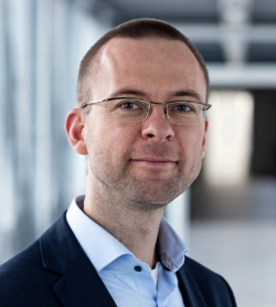
Gabriel Kittler

Gabriel Kittler
CEO Site Erfurt
X-FAB Semiconductor Foundries GmbH

Biography
Gabriel Kittler ist Site CEO of X-FAB in Erfurt (Germany). From 2012 to 2020 he coordinated as Innovation Manager all activities concerning emerging technologies and collaboration with universities, research centers, and industrial partners. In 2007 he started in the Process Development at X-FAB with focus on TCAD simulations for HV devices at different technology nodes. He studied Electrical Engineering with focus on Microelectronics at the Technical University of Ilmenau and holds a Ph.D. in Electrical Engineering and Information Technologies.

14:10
Advanced Photonic Integrated Circuits Solutions with Integrated Lasers for Ultimate Optical Connectivity in Datacenters, HPC and 5G
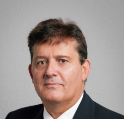
  Pascal Langlois, Chairman of the board, Scintil Photonics
Advanced Photonic Integrated Circuits Solutions with Integrated Lasers for Ultimate Optical Connectivity in Datacenters, HPC and 5G
Pascal Langlois

Pascal Langlois
Chairman of the board
Scintil Photonics

Pascal Langlois

Abstract
Scintil Photonics develops and markets Photonic Integrated Circuits (PICs): integrated laser arrays, multiples of 800 Gbit/sec transmitters and receivers, tunable transmitters, and receivers, as well as optical I/O for near chip and chip-chip communication). Its circuits are fabricated on a proprietary III/V-Augmented Silicon Photonics technology manufactured in a multi-customer silicon foundry. For accelerated adoption, the company also delivers the control electronics and reference package implementations. Based in Grenoble, France, and Toronto, Canada, Scintil is currently taking its innovative product to industrial level as it gears up for mass production. www.scintil-photonics.comUnique value proposition Scintil Photonics is focusing its efforts on ultra-high speed optical communication circuits for Datacenter interconnect and High-Performance Computing cloud systems. We deliver sustainable data rate, high volume production capability, while offering 40 percent power reduction.Value chain As a supplier of optical components, our circuits integrate all the optical components required to make an optical communication (lasers, modulators) We sell our circuits to equipment manufacturers in networking or high-performance computing equipment or we can sell them customers which integrate our circuits into modules. Our customers directly sell their equipment or modules to datacenters and telecom operatorsUnique technology We develop Disruptive Photonic Integrated Circuits for ultra-high-speed optical communications, exploiting a technology developed at Cea Leti. We have demonstrated high performance prototypes fabricate from our commercial foundry over the last 3 years. Some successful reliability tests were performed on our prototypes have proven reliability of the technology. SCINTIL circuit technology combines the best of III-V material and silicon photonics by molecular bonding III-V material at the backside of an already processed silicon photonic wafer. This makes us uniquely capable of integrating multiple lasers on advanced silicon photonic circuits and because one laser can carry 100 Gbit/sec and more, we can deliver ultra-high speed performances and our circuit technology leverages silicon photonic processes available in several commercial foundries. Therefore, our circuits can be supplied in volume.

Biography
Pascal LANGLOIS cofounded Scintil Photonics on November 2018 with Sylvie Menezo president and CEO. He is serving as chairman of the board. Most recently, Langlois was President and CEO of Tronics Microsystems, a Mems company he introduces in 2015 on Euronext Stock market, and which was acquired by TDK Group end of 2016. Prior to that he was Chief Sales and Marketing Officer at ST-Ericsson and from 2006, Founder of NXP and part of the executive management team responsible for global sales. He was previously with Philips Semiconductors BV, where he served in various capacities, including Senior VP of Sales and Marketing for multimarket products and VP of the automotive global market segment. He also worked with VLSI Technology, where his last position was VP for Europe, Asia Pacific and Japan operations. Pascal graduated with a Bachelor in technology from the University of Paris, and attended strategy and organization executive program from Stanford University. Langlois is also Chairman of supervisory board of Teem Photonics, an industrial laser company and Director of Yole Development, a market research firm.

14:30 Reserved for iPronics, Programmable Photonics
14:50
Heterogeneously Integrated InP-laser on Silicon Photonics realized by Micro-Transfer Printing
  Samir Ghosh, Researcher, Tyndall National Institute
Heterogeneously Integrated InP-laser on Silicon Photonics realized by Micro-Transfer Printing
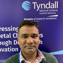

Samir Ghosh

Samir Ghosh
Researcher
Tyndall National Institute

Samir Ghosh

Abstract
Silicon photonics have gained immense commercial interest in data-center market and soon it will enter other domains as well including biomedical, space applications and so on. Silicon being an indirect bandgap semiconductor efficient lasing cannot be achieved. Therefore, hybrid or heterogeneous integration techniques are normally used to incorporate laser with silicon photonics (SiP) platform. These techniques of integrating lasers on SiP platform are far from ideal in-terms of volume, cost and yield. Micro-transfer printing is an emerging technology which enables massively parallel integration with high yield and hence bring the cost down. In this talk transfer printing of InP-based laser on SiP chip will be presented.

Biography
Samir Ghosh obtained his Ph.D. degree in Photonics Engineering from Ghent University, Gent, Belgium in 2013. Afterwards he worked at various academic institutes as a postdoctoral researcher including McGill University – Canada, University of California - Davis, The University of Tokyo - Japan, and Nanyang Technological University - Singapore. Since October, 2020 he is working as a researcher at Tyndall National Institute, Cork, Ireland where his primary interest lies on heterogeneous integration of InP, LN-based devices on Si-Photonics platform utilizing micro-transfer printing technology. His has (co-) authored of 30 publications in referred journals and in international conference proceedings. His broad research interests include large-scale photonic integrated circuit for communication, sensing and imaging applications.

15:10
Next Generation Microchips, Powered by Light
  René Penning de Vries, Chairman of the Supervisory Board, PhotonDelta
Next Generation Microchips, Powered by Light
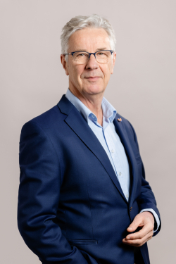
René Penning de Vries

René Penning de Vries
Chairman of the Supervisory Board
PhotonDelta

René Penning de Vries

Abstract
Coming soon

Biography
René Penning de Vries, PhD, has been employed by Royal Philips NV and subsequently NXP Semiconductors as Chief Technology Officer and as CEO of NXP Netherlands.Since 2012 René has taken up various public sector roles with the aim of fostering of innovation. René has acted a Chairman of various initiatives such as Dutch Digital Delta, Health Valley and the BOM (Regional Develpoment Agency for the province of Brabant).Currently René is chair of the SVB of the St Maartenskliniek, a specialized clinic for posture and movement. Next to this, René is involved with the Novio Tech Campus in Nijmegen and advises the Knowledge and Innovation Committee (KIC) in NWO (Netherlands Organisation for Scientific Research).Since early 2018, René is the Chairman of the Supervisory Board of PhotonDelta, which oversees the national initiative on Integrated Photonics.

15:30
Silicon Nitride based low loss Photonics Integrated Circuits
  Thomas Hessler, CEO, Ligentec SA
Silicon Nitride based low loss Photonics Integrated Circuits

Thomas Hessler
CEO
Ligentec SA

Abstract
SiN has been in discussion for a long time as the perfect material for integrated photonics due to its low propagation losses, but SiN layers were limited in thickness. LIGENTEC has developed a unique way to manufacture thick SiN layers and offers a set of SiN layer stacks for different applications. This enables the manufacturing of PICs at much lower losses, better performance, and lower cost than other common approaches. In addition, LIGENTEC’s processes for the thick SiN have been developed to be fully compatible with standard CMOS equipment, thus allowing it to leverage existing infrastructure from the semiconductor industry.We will present the LIGENTEC offering for low loss silicon nitride PICs for applications such as quantum computing, LiDAR sensors for autonomous driving and biomedical sensing applications. Options of active integration are discussed. The offering includes fast R&D cycles in low volume PIC fabrication though multi-project wafer runs to high volume PIC fabrication in an automotive qualified CMOS line.

Biography
Thomas Hessler CEO of LIGENTEC SA, a Swiss rooted company providing low loss Photonic Integrated Circuits. Prior to LIGENTEC, he was a general manager of Axetris AG. He grew this high-tech corporate start-up as employee No 1 and developed it to a market segment leader in wafer level micro-optics and optical gas sensing for communication, medical, industrial, and automotive applications. He studied physics at Constance University and got his PhD in Applied Optics with the Institute of Microtechnology, University of Neuchâtel and the Paul Scherrer Institute. Thomas has a broad experience in various fields of photonics and sensors, including free space, refractive and diffractive micro-optics, optical gas sensing, laser spectroscopy, microfluidics, cell analytics, and integrated photonics. He is also a Member of the Board of Swissphotonics Association and MIRO Analytical AG, a environmental gas monitor company.

15:50
Label-Free Biomarker Sensing Leveraging CMOS Technology and Photonic Integration
  Leo Grünstein, CEO, Spiden AG
Label-Free Biomarker Sensing Leveraging CMOS Technology and Photonic Integration
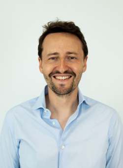
Leo Grünstein

Leo Grünstein
CEO
Spiden AG

Leo Grünstein

Abstract
Today, biomarkers such as urea, lactate, glucose and others are commonly sensed invasively and non-continuously. Spiden's vision is to extend human longevity through its proprietary sensing platform. It allows to measure various biomarkers without the need for fluorescent markers or surface functionalization. This enables real-time and continuous measurements of analytes within patients matching one of the most prevalent medical needs.In this talk, we will describe our recent advances in the field of label-free biomarker sensing.Here, we will discuss our preliminary measurement data of our integrated CMOS spectroscopy detector in comparison to state-of-the-art spectroscopy measurement equipment.An outlook is given about future products using photonic integration and potential routes for the implementation of transcutaneous wearable devices. We will also discuss the current photonic eco system relevant for our applications. In this context we highlight the missing technology platforms, which still hamper the wider spread use of point-of-care and wearable biomedical sensing applications.

Biography
Leo Grünstein is a serial entrepreneur. With his Swiss-based venture builder LG Capital he co-founded 20 ventures from the ground up, raised >600m CHF for them, sold more than half of them successfully (e.g. MoneyPark that was acquired to 70% by Helvetia Insurance for a valuation of CHF 153m in 2017), with the rest either having failed or still being up-and-running. He is the founder and CEO of Spiden, in which Leo found his passion focusing on longevity and health. Spiden is working on the difficult problem of transcutaneous non-invasive sensing of multiple biomarkers. The company built and uses its super-spectral engine + AI to analyse biomarkers and drugs for the first time optically, in-flowing biological fluids (e.g. blood) with the goal to create a unique next-generation wearable device to provide access to unseen biomarker data and help to extend human longevity.Jens Hofrichter, PhD, has 15 years of experience in integrated photonics R&D. He drove the development of the passive components, wafer-level test infrastructure and monolithic laser integration of silicon photonics at IBM contribution to the 100Gbit/s LR4 transceiver. In 2015 he moved to ams, where he was setting up the fully automated optical product validation and optical wafer-level testing capabilities for medical and specialty products. He was in charge of the radiation hard monolithic photodiode development, which led to the development of monolithic computed tomography chips used in 16 and 32 slice CT scanners. He was leading the hybrid bonding development for non-Cu hybrid bonded imaging sensors. After that he was leading the cross-divisional camera team for the development of miniature AR cameras. As co-inventor of the optical microphone, he was appointed program manager of the related industrialization program in the ams-Osram group. In 2022 he moved to Spiden, where he is currently leading the optical and photonic integration activities for next-gen medical sensors. He is the (co)author of more than 30 patent families mainly in the field of photonic integration and imaging sensors.

16:10
Packaging for Integrated Photonics
  Bradford Factor, Director, Packaging Technology, ASE Europe
Packaging for Integrated Photonics


Bradford Factor

Bradford Factor
Director, Packaging Technology
ASE Europe

Bradford Factor

Abstract
Coming Soon

Biography
Bradford Factor received his Ph.D. from Stanford University in Applied Physics in 1991 and worked in research in France and Greece, and at the Polymers Division of NIST in Maryland, USA. Bradford began his career in the semiconductor packaging the mid 1990’s, first at Intel and then at Lucent Microelectronics in BGA and flip chip materials and assembly. He subsequently worked on packaging of planar waveguide circuits and optoelectronic devices at Corning in France. Since joining ASE Europe in 2002, he supports the European customer base focusing on advanced technologies, including flip chip, wafer level and fan-out packaging, system-in-package as well as power packaging. He is a currently a board member of the IEEE EPS chapter in France, and has received several patents and published several journal articles.