Wednesday, November 16, 2022
 

Session 1: Updates from the Semiconductor Back-End Assembly Market in Europe

08:30
Welcome Note
  Cassandra Melvin, Senior Director of Business Development & Operations, Semi Europe
Welcome Note

Cassandra Melvin

Cassandra Melvin
Senior Director of Business Development & Operations
Semi Europe

Cassandra Melvin

Abstract
Coming Soon

Biography
Coming Soon

08:35
Opening Remarks
  Steffen Kröhnert, President & Founder, ESPAT-Consulting
Opening Remarks
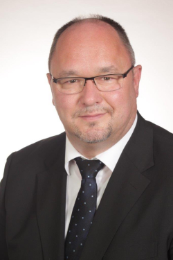

Steffen Kröhnert

Steffen Kröhnert
President & Founder
ESPAT-Consulting

Steffen Kröhnert

Abstract
N/A - Session 1 - Opening Remarks

Biography
Steffen Kroehnert is President & Founder of ESPAT-Consulting based in Dresden, Germany. He is providing a wide range of consulting services around Semiconductor Packaging, Assembly, and Test. Until June 2019, he worked for more than 20 years in different R&D, engineering, and management positions at large IDMs and OSATs in Germany and Portugal, namely Siemens Semiconductors, Infineon Technologies, Qimonda, NANIUM, and Amkor Technology, where he served as Senior Director Technology Development. Since 2012 Steffen is chairing or co-chairing the "Advanced Packaging Conference" (APC) at SEMICON Europa. Since 2016 Steffen is chairing or co-chairing the "European SEMI integrated Packaging, Assembly, and Test - Technology Community" (ESiPAT-TC). Steffen has authored or co-authored 23 patent filings and many technical papers in the field of Packaging Technology. He co-edited two books about Embedded and Fan-Out Wafer and Panel Level Packaging Technologies. He is an active member of several technical and conference committees of IEEE EPS, where is was elected to the Board of Governors (2021-2023) for Region 8 (EMEA), IMAPS, SEMI Europe, and SMTA. Steffen holds an M.Sc. in Electrical Engineering and Microsystems Technologies from the Technical University of Chemnitz, Germany.

08:40

Keynote

 
Building Europe’s Digital Future - A Pan European Investment
  Frans Scheper, Corporate Vice President in the Sales and Marketing Group General Manager and President EMEA, Intel Corporation
Building Europe’s Digital Future - A Pan European Investment
Frans Scheper

Frans Scheper
Corporate Vice President in the Sales and Marketing Group General Manager and President EMEA
Intel Corporation

Frans Scheper

Abstract
Building Europe’s Digital Future - A Pan European Investment

Biography
Frans Scheper is Corporate Vice President in the Sales and Marketing Group General Manager and President, for Europe, Middle East and Africa (EMEA) for Intel Corporation.Frans is responsible for Intel’s overall business in EMEA which includes driving revenue growth, engaging with the local ecosystem to create new opportunities, and strengthening Intel’s existing regional customer and partner relationships.As President, Frans oversees Intel’s recently announced plans for the “once-in-a-generation” investment in Europe as part of its IDM 2.0 strategy, with research, design, leading-edge semiconductor manufacturing and industry partnerships that will help build Europe’s digital future.Frans recently joined Intel (2022) from ams OSRAM, where he was Chairman and Executive Vice President of Opto Semiconductors. He brings extensive European and international market experience, having also held executive board positions at WeEn Semiconductors, NXP Semiconductors and the CEO position at Nexperia.Based in the Netherlands, Frans holds a bachelor’s degree in business and commerce from HES Den Haag, and an MBA from the International Institute for Management Development (IMD).

09:05

Keynote

 
Semiconductors for Software Defined Vehicles
  Leopold Beer, VP Product Management ASIC's & SOC's, Robert Bosch GmbH
Semiconductors for Software Defined Vehicles
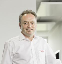
Leopold Beer

Leopold Beer
VP Product Management ASIC's & SOC's
Robert Bosch GmbH

Abstract
The importance of SW in Automotive is constantly increasing and currently we are reaching a point where its justified to talk about software defined vehicles.In his talk, Leopold will elaborate why semiconductors became a special focus topic for automotive OEM's and what this means for the traditional automotive semiconductor and system suppliers. At this stage of evolution, traditional, hirarchical supply chains restructure into to supply networks - opening up opportunities for new players.Based on technology requirements, Leopold will show how this new structures could look like and which are the new Key Succes Factors for the involved players.Leopold will use real life examples to explain the way Bosch Automotive Electronics addresses this topic.

Biography
Mr. Leopold BeerVP Product Management ASIC’s and SOC’s within the Bosch Automotive Electronics Division.Leopold Beer graduated the University of Stuttgart with a diploma in Physics. He specialized in semiconductor physics.Leopold started his career as engineer in the DRAM plant of Siemens Semiconductors (Today Infineon Technologies) in Regensburg and since then held various functions in the automotive and semiconductor industry.Leopold joined Bosch Sensortec in 2006 as Director of Sales and was later on promoted to Head of Global Marketing and Product Management. From 2013 to 2018 Leopold held the position of Regional President for Asia Pacific and was based in Shanghai/China. Since August 2018, Leopold oversees the ASIC & SOC product portfolio of Bosch Automotive Electronics.

09:30

Keynote

 
Amkor Activities in Portugal and Overall Trends in Europe
  José Silva, Vice President of Operations & R&D, Amkor Technology Europe Portugal (ATEP)
Amkor Activities in Portugal and Overall Trends in Europe
José Silva

José Silva
Vice President of Operations & R&D
Amkor Technology Europe Portugal (ATEP)

José Silva

Abstract
Coming soon

Biography
José joined Amkor in July 2017 as part of the Nanium acquisition and is currently Vice President of Operations & R&D at ATEP. He started his career in the semiconductor industry at Siemens and later held management positions as Quality Director and Operations Director at Infineon, Qimonda and Nanium. José holds a degree in Electrical Engineering from Universidade do Porto and an MBA from Porto Business School.

09:55

Coffee break


Session 2: 3D Packaging Trends, Design and Assembly

10:25
Opening Remarks
  Roland Rettenmeier, Senior Product Marketing Manager, Evatec AG
Opening Remarks
Roland Rettenmeier

Roland Rettenmeier
Senior Product Marketing Manager
Evatec AG

Roland Rettenmeier

Abstract
not applicable

Biography
Roland Rettenmeier qualified as a Mechanical Engineer in 1997 and completed his MBA studies at Vienna and Danube Universities in Austria in 2005. Roland extended his education through many further formal international courses and programs since that time (e.g. Six Sigma Program with AT&S and Nokia; Innovation Technology Leader at Stanford University).Roland has worked in the field of Electronics and Semiconductor manufacturing since 2001, managing multiple international projects. After joining Evatec in 2016 as Senior Product Marketing Manager (PMM) within the Business Unit for Advanced Packaging, he focused on business development for Panel Level Packaging where Evatec has now become the recognised market leader for thin film technology solutions. Since 2020 he has also supported development of Evatec’s wafer level packaging solutions business.In addition to his market and customer responsibilities, Roland represents Evatec in the Panel Level Packaging consortium of Fraunhofer IZM Berlin, in the Packaging Research Center at Georgia Tech, USA and in the Panel Level Packaging Consortium at the NCAP in Wuxi, China.

10:35

Keynote

 
Advanced Packaging: Enabling a New Generation of Silicon Systems
  Yin Chang, Sr. Vice President, Sales & Marketing, ASE, Inc.
Advanced Packaging: Enabling a New Generation of Silicon Systems
Yin Chang

Yin Chang
Sr. Vice President, Sales & Marketing
ASE, Inc.

Yin Chang

Abstract
Demand for new efficiencies in the semiconductor design and manufacturing process is propelling the crucial role of packaging to deliver on requirements related to miniaturization, power, and performance. During his keynote presentation, Yin Chang will explore heterogeneous integration and chiplet innovation, and describe how advanced packaging technologies are enabling highly complex system integration. With applications such as automotive and power management demanding significant attention, he will highlight solutions that are helping create a smarter and more sustainable world for generations to come.

Biography
Ingu Yin Chang is Senior Vice President, Sales & Marketing, at ASE, based in Sunnyvale, California. In his current role, he is responsible for developing and executing sales strategy, while driving marketing activities for ASE’s expanding packaging, systems, and integration solutions portfolio.Prior to joining ASE in 2013, Yin was CEO of Vertical Circuits Inc. (VCI), a company focused on the development of next generation vertical interconnect for next generation silicon integration. Previously, Yin performed a variety of management roles covering sales and operations at Amkor with responsibility for the Greater China region. He has over twenty years of leadership experience in executive management, sales, business development, IP management and strategic alliance.Yin received his material science engineering degree from University of California, Berkeley.

11:00
Complete LVS verification methodology and process for complex System-In-Package assemblies
  Raphael Theveniau, CAD Support Senior Staff Engineer, ST Microelectronics
Complete LVS verification methodology and process for complex System-In-Package assemblies
Raphael Theveniau

Raphael Theveniau
CAD Support Senior Staff Engineer
ST Microelectronics

Raphael Theveniau

Abstract
Systems in Package (SiP) have been around for some years and were typically the integration of multiple bare unpackaged chips along with discrete devices interconnected with just a few signals. However, as silicon scaling (aka Moore’s Law) slows and silicon densities reach their physical limits, there is growing shift to disaggregation of once monolithic functions into smaller, node optimized high yield chiplets, heterogeneously integrated on a high-performance substrate as an advanced System-In-Package (SiP), or module. These designs utilize multiple high performance and high bandwidth interfaces between the chiplets enabling higher densities, greater device functionality, and improved overall silicon yield. All the devices used in a SiP are often designed concurrently, by different teams, in different time zones. Thus, the risk to make mistakes in data exchange is very high. To mitigate this risk a comprehensive system description along with a controlled data exchange flow is key. Furthermore, although each device is tested independently, there is a need for a formal signoff check or verification that covers the whole system.In STMicroelectronics we have developed an automated layout versus schematic (LVS) methodology that electrically verifies the module and system-level designs logical connectivity. Using a combined 3D assembly level DRC/LVS methodology our divisions can prevent System in Package failures due to swapped balls, shorted power nets or any uncontrolled change in the design layouts.This paper will describe the essential steps and process of a fully integrated workflow that can verify and validate a complete multi-chiplet SiP design assembly using an LVS approach including the technologies used to enable such a solution.

Biography
After 5 years spent in Cadence UK and 5 years in Texas Instruments France, Raphael Theveniau joined STMicroelectronics in 2009 as System in Package expert. He is now part of Technology R&D group in ST, in Digital Design Flows and Methodology team. He has more than 20 years of experience in Digital Design, covering most aspects of place and route and signoff flows and package design. His role as SiP expert consists in developing, promoting and supporting flows through ST kits for internal divisions as as well as external customers. Now his role is more focused on Die-Package Co-design flows, and more specifically System in Package LVS.

11:25
Ultra-fine pitch Die bonding approaches with Cu interconnects for high-performance 3D IC packages
  Ali Roshanghias, staff scientist, Silicon Austria Labs GmbH
Ultra-fine pitch Die bonding approaches with Cu interconnects for high-performance 3D IC packages
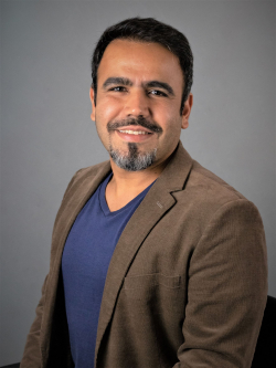
Ali Roshanghias

Ali Roshanghias
staff scientist
Silicon Austria Labs GmbH

Ali Roshanghias

Abstract
Cu to Cu direct bonding is currently the most attractive approach for 3D integration due to its compatibility with the wafer back-end-of-the-line (BEOL) fabrication process. Direct or hybrid Cu bonding is an established wafer-to-wafer (w2w) bonding process at foundries. However, considering the increasing demand for heterogeneous chip stacking and high production yield with known good die (KGD), chip-to-chip (C2C), and chip-to wafer (C2W) Cu bonding processes still encounter technological challenges. In this study, we will explore different die-level bonding strategies for both protruded and recessed Cu interconnects. Here, Cu bumps with a diameter of 4 µm, and a pitch size of 18 µm surrounded by SiO2 layer were fabricated with different topographies (dishing heights) and were bonded at the different bonding temperatures. The results of the electrical examinations, bonding strength, texture, and interface analysis will be further discussed here.

Biography
Dr. Ali Roshanghias is currently a staff scientist in the department of heterogeneous integration technologies at Silicon Austria Labs (SAL). He received his Ph.D. in materials science and technology from Sharif University of Technology (Iran) in 2012. He pursued his career as a post-doc researcher at Nagaoka University of Technology (Japan) and Vienna University (Austria) in the fields of electronic materials and advanced microelectronics packaging. In 2015 he joined Silicon Austria Labs (formerly known as CTR Carinthian Tech Research AG) as a senior scientist and project manager. His research interests include heterogeneous integration technologies, hybrid electronics, and 3D integration.

11:50
Optimization of the Cu Microstructure to Improve Cu-to-Cu Direct Bonding for 3D Integration
  Ralf Schmidt, R&D Manager Semiconductor, Atotech
Optimization of the Cu Microstructure to Improve Cu-to-Cu Direct Bonding for 3D Integration

Ralf Schmidt
R&D Manager Semiconductor
Atotech

Ralf Schmidt

Abstract
Advanced packaging solutions and heterogeneous integration are key technologies to enable devices with improved operating characteristics, including higher performance, increasing power efficiency, and decreasing form factor. Packages with high I/O densities are required to efficiently combine, e.g., processing and memory units but impose restrictions to the pitch of the interconnects. Conventional technologies, including wire bonds and flip chip bonds are limited to larger pitches and, therefore, not suitable to meet the requirements of upcoming packaging technologies with respect to I/O densities. Direct copper-to-copper interconnects are supposed to allow such small pitches of 10 µm or even below. However, formation of such bonds usually requires high temperatures and pressures. Temperature-sensitive devices like DRAM components restrict the maximum temperature that can be applied to the package. Thus, copper material is required, which allows bond formation at relatively low temperatures. In this context, hybrid bonding processes were discussed that involve initial bond formation via the usually oxide-based dielectric at room temperature followed by copper-to-copper bonding at elevated temperatures. The copper material is usually prepared by electrolytic deposition and the properties of the respective deposits may be modified by properly designed organic additives as well as process parameters. Strong bond formation of the copper should be obtained upon grain growth over the interface of the two deposits, which are brought into contact during the bonding step. In order to facilitate such growth at relatively low temperatures, suitable microstructures need to be prepared. Ideally, morphologies should be chosen in a way that they can be maintained throughout all process steps after the electrolytic deposition but, at the same time, allow grain growth over the interface during copper-to-copper bonding. Various strategies to enable improved seamless grain growth and maintain suitable microstructures throughout the preceding process steps will be compared in terms of the resulting copper microstructures after bonding. In this context, different electrolytic copper deposition processes, the resulting morphologies, as well as their respective advantages and challenges with regards to copper-to-copper bond formation will be discussed.

Biography
Experience with process development for semiconductor applications since 2016Author of numerous scientific publications and patents in the area of metallization for semiconductor applications.Lecturer at the Humboldt University of Berlin since 2013Experience with metallization processes for electronics industry for > 10 years

12:10

Lunch break

12:10

Posters at break out area

 
Ultra low-temperature silver sintering materials for substrate-based power applications
  Rui-Xuan Dong, Project Leader, Niching Industrial Corp.
Ultra low-temperature silver sintering materials for substrate-based power applications

Rui-Xuan Dong
Project Leader
Niching Industrial Corp.

Rui-Xuan Dong

Abstract
The demand of high powder semi-conductor devices is increasing continuously. Especially for wide band gap (WBG) semiconductors, the die-attach (DA) materials need to be bonded at a lower temperature,200 oC ideally, and operated at a high temperature (~300oC). Low-temperature sintering silver provides excellent properties to meet the requirement of DA materials on WBG applications. The common sintering temperature of commercial products is > 200dC. High sintering temperature generates a higher level of thermal stress in the DA materials, which would cause negative effects for larger dies, including void generation, delamination, crack, metallization peeling, and so on. Lower sintering temperature could reduce thermal stress during packaging processes. In addition to 200-oC sintering Ag paste (DN-1206Q), we have developed DA Ag paste with 175-oC sintering temperature (DN-1301A) for the requirement of low stress. This article is investigating the effect of sintering temperature on the performance and properties of DA materials.The storage modulus of 175oC (DN-1301A) and 200oC (DN-1206Q) sintering Ag paste are 14 and 18 GPa respectively. This is more than 20% reduction which could be a great help in terms of thermal stress. As for die shear strength (DSS), DN-1301A showed comparable results while curing at 175 oC comparing with DN-1206Q curing at 200 oC. Thermal conductivity (TC) of both 175 and 200-oC sintering Ag paste is more than 120 W/mk. In summary, lower sintering temperature can reduce the thermal stress of DA materials which is a positive contribution to the resistance of temperature variations. The performance of DN-1301A curing at 175 oC is similar to 200oC sintering Ag paste (DN-1206Q). Based on this study, it is very promising that a lower sintering temperature at 175 oC for silver sintering paste can deliver similar performance as curing at 200 oC. This could be a breakthrough for those requiring lower curing temperature such as laminate substrate-based packages.

Biography
2006-2010 Ph.D, Institute of Polymer Science and Engineering, National Taiwan University.2014-2016 Researcher, Industrial Technology Research Institute2016-2019 R&D Manager, New Micropore, Inc.2019-Now R&D Project Leader, Niching Industrial Co.

13:10

Gaming with ASE – Your chance to win AirPods Pro!

  Thanks to our sponsor, ASE, we will be giving away three AirPods Pro sets in the APC at 13:40!
13:15

Panel Discussion: Future of semiconductor manufacturing in Europe: Back –end Packaging and Test


Session 3: Advanced Packaging Materials and Reliability

13:40
Opening Remarks
  Pascal Oberndorff, Research Director, NXP
Opening Remarks
Pascal Oberndorff

Pascal Oberndorff
Research Director
NXP

Pascal Oberndorff

Abstract
Not applicable

Biography
Coming Soon

13:50

Keynote

 
Semiconductor Packaging Materials Enabling Advanced Flip-Chip and Heterogeneous Integration
  Ramachandran Trichur, Global Head of Semiconductor Packaging, Henkel Corporation
Semiconductor Packaging Materials Enabling Advanced Flip-Chip and Heterogeneous Integration

Ramachandran Trichur

Ramachandran Trichur
Global Head of Semiconductor Packaging
Henkel Corporation

Ramachandran Trichur

Abstract
In recent years, semiconductor chip package architectures have become more complex to deliver various applications’ power, performance, size, and cost requirements. Chipsets used in consumer electronics devices such as mobile phones and handheld electronics predominantly require miniaturization, high functionality, low cost, and low power. Therefore, the packages specified for this market segment may include package-on-package (PoP) formats to save space or wafer-level packages (WLP) to deliver lower cost and, in many cases, higher functionality. In comparison, processors used in high-performance computing (HPC) and artificial intelligence (AI) applications place a premium on performance while balancing cost, power, and footprint. Because of these factors, packaging architects have developed several custom package formats like chiplets, large-die flip-chip, and multi-chip packages in 3D and 2.5D, among others. Both end markets require unique innovations in semiconductor packaging materials to enable efficient package production and in-application performance. While package designs have come a long way, challenges to meeting new, demanding requirements persist. Advanced packaging material solutions are central to addressing these issues.Liquid compression molding materials are predominantly used in fan-out or chip-on-wafer packaging for wafer-level encapsulation processes. As the interconnect density or stacking height increases, fine-filler, low-warpage materials are necessary to deliver the package's reliability and the wafer's processability. In AI and HPC applications, the package body size increases with subsequent generations. These large body packages are susceptible to thermal stresses resulting in warpage and reliability concerns. Component level adhesives like lid and stiffener attach materials must be able to manage/prevent warpage while maintaining good adhesion and reliability performance. Lastly, underfills also play a crucial role in packaging logic and memory devices. Pre-applied and post-applied underfill in liquid and film formats are needed to address challenges in flow time, interconnect density, voiding, crack formation, and various other issues. This Keynote will present the latest innovations in encapsulation materials used for fan-out wafer-level molding processes, alongside developments in advanced liquid underfills and lid/stiffener attach materials.

Biography
Coming soon

14:15
GlobalFoundries 22FDX® Auto grade 1 Chip Package Interaction Reliability Assessment
  Simone Capecchi, MTS Reliability, GlobalFoundries
GlobalFoundries 22FDX® Auto grade 1 Chip Package Interaction Reliability Assessment
Simone Capecchi

Simone Capecchi
MTS Reliability
GlobalFoundries

Simone Capecchi

Abstract
Semiconductor devices are becoming every year more pervasive in the automotive industry. Moreover, the growth of the Electrical Vehicle (EV) market in addition to new features such as Advanced Driver Assistance Systems (ADAS), Lidar and auto connectivity is accelerating this trend. The value of the market for automotive semiconductors applications is set to grow from about $35B in 2020 to about $80B in 2026 (~15% CAGR) and it is expected to reach about $300B by 2035*. Therefore, this tremendous growth has generated an increased interest for semiconductors IDMs and foundries to enter or strengthen their presence in the automotive supply chain.In this work we present a chip package interaction (CPI) Automotive Grade1 reliability assessment performed onto to a GlobalFoundries 22FDX® technology test vehicle. The presentation will focus mainly on the temperature humidity bias life test (THB), which is one of the AEC-Q100 requirements. The aim of the CPI assessment is to prove that the GlobalFoundries 22FDX® back-end of line metallization (BEoL) the passivation and the Far BEoL interconnects are robust enough in an Auto G1 standard package and can withstand the AEC-Q100 grade 1 reliability environmental stresses.For this purpose, a test vehicle has been designed and fabricated by GlobalFoundries Fab1 including the Cu pillar interconnects. The subsequent packaging has been carried out by an external Auto G1 qualified OSAT using their Auto G1 HVM bill of material (BOM) and assembly process. The environmental stresses and electrical readout have been carried out in GlobalFoundries Fab1.The test vehicle is a 22FDX® 8x8 mm2 silicon die assembled in a 14x14 mm2 Flip Chip Chip Scale Package (FCCSP) with an Embedded Trace Substrate (ETS) coreless substrate. This test vehicle contains various kinds of CPI sensors distributed in sensitive die locations.Compared to the component level reliability stress, which is also carried out as part of the CPI assessment, the THB assessment requires a dedicated board level stress and a dedicated test infrastructure. The THB adapter card assembly process, the electrical test pre and post stress and the THB reliability environmental stress have been set up and carried in GlobalFoundries Fab1.The focus of this presentation is on the technical challenges, such as the CPI structure design, the THB board and adapter card design, the electrical readout, and the adapter card assembly.*Source: Yole Développement

Biography
I am currently a member of the quality and reliability group in GlobalFoundries Fab1 in Dresden, Germany. The main focus of my activity is Chip Package Interaction (CPI) reliability. I have previously worked in process engineering in Globalfoundries, ST-Microelectronics and in Intel.I hold a Master's Degree in Physics

14:40
Reliability Characterization of Silver Sintering for Die Attach Applications
  Edsger Smits, Program Manager, CITC
Reliability Characterization of Silver Sintering for Die Attach Applications
Edsger Smits

Edsger Smits
Program Manager
CITC

Edsger Smits

Abstract
With advances in miniaturization of electronic components, there is a trend towards ever increasing power density in semiconductor devices. In part, Wide-Band Gap (WBG) materials such gallium nitride (GaN) and silicon carbide (SiC) have enabled more efficient devices but also allowed for much higher operating temperatures. Consequently power dissipation and mechanical stresses in electronic packages have increased dramatically. From environmental perspectives, there is a strong drive to phase out lead-based solder.Discrete components are commonly assembled in packages based copper lead frames. The key challenge for such packages are the mismatches in coefficient of thermal expansion (CTE) between Cu lead frame and WBG power dies. During operation, the packages repeatedly undergo temperature swings, causing repeated thermomechanical stresses and fatigue. When not mitigated, these stresses lead to premature failure of the electronic components.Silver Sinter pastes (pressure based and pressureless) are a promising replacement of lead rich solder combining superior thermal and electrical performances. It is the scope of major research activity but a reliable solution for attaching WBG semiconductors to copper bases while retaining superior thermal and electrical performances has proven to be challenging. Unlocking the full potential of WBG semiconductor power electronics will hinge on solving these technological challenges at the package level.In this presentation, the author presents an overview of CITC research activities on advanced packaging with a focus on packaging for power electronics and silver sintering solutions. An overview of the current state of silver sinter materials is provided. The performance and limitations of the materials are addressed. Beyond materials, methods used to investigate the performances and degradation will be covered as well as the thermomechanical simulations for predicting package reliability.

Biography
Edsger Smits received his Ph.D. with honors from the University of Groningen in the field of organic electronics. In 2009, he joined TNO/Holst Centre focusing oxide based thin film transistors for displays, flexible and stretchable sensors and electronics for bio-medical applications. In 2021 he become responsible for the “Power Packaging “ at CITC. Topics of interests include mini and micro led, laser transfer, flexible and stretchable electronics and power packaging.

15:05
HFBP as a New and Better Approach to DFN
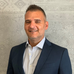
  Mark Azzopardi, Business Development Engineering, JCET
HFBP as a New and Better Approach to DFN
Mark Azzopardi

Mark Azzopardi
Business Development Engineering
JCET

Mark Azzopardi

Abstract
Coming Soon

Biography
Mark Azzopardi has been building semiconductor packaging experience for just over 20 years, after getting his Engineering degree in Mechanical engineering from the University of Malta in 2002. He started his career as a process engineer and moved to R&D for SiP and MEMS packaging. Mark then joined Statchippac, now JCET, in 2011 as technical program manager and moved to Business Development supporting the European local sales team early 2022.

15:30

Coffee break


Session 4: System-in-Package Trends, Assembly and Test

15:55 Opening remarks
  Roberto Antonicelli, Automotive BU, JCET
Roberto Antonicelli

Roberto Antonicelli
Automotive BU
JCET

Biography
Roberto Antonicelli is a professional with over 20 years of experience in the semiconductor industry. At JCET Group, formerly STATS ChipPAC, he is in charge of the Automotive BU for US and Europe. He is based in Morges (Switzerland), on the shores of the Leman Lake. Prior to joining STATS ChipPAC in 2010, he has held diverse R&D positions at Infineon Technologies, Alcatel Microelectronics and ST Microelectronics. Roberto obtained his MSEE and PhD from Polytechnic University of Bari, Italy, respectively in 1997 and 2002.

16:00

Keynote

 
Innovative Sensor Packaging in Europe
  Bernhard Knott, Head of the Infineon Technologies Backend Innovation Group, Infineon
Innovative Sensor Packaging in Europe
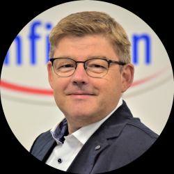

Bernhard Knott

Bernhard Knott
Head of the Infineon Technologies Backend Innovation Group
Infineon

Bernhard Knott

Abstract
The presentation will include topics like: eWLB radar (fan-out WLP at Infineon Regensburg); Pressure sensors e.g. for automotive; Magnetic sensors and Gas sensors.

Biography
Bernhard Knott is the Head of the Infineon Technologies Backend Innovation group. He is responsible for new Package Concepts, Prototyping, new Materials, Simulation and Virtual Prototyping. Until 2016 he was leading the Package Development for Sensors and Waferlevel Package Development in Regensburg, Germany. Prior joining the Backend Organization, he held several Management Position in Frontend Technology dealing with BiCMOS Technologies, Sensors and Innovation projects. After receiving his Diploma in Physics from the University of Regensburg, he started his career in Semiconductor Industry in 1997 in developing an embedded NVM Technology. Bernhard holds several patents and patent applications in the area of FE Technology, Sensors and Packaging.

16:25
Impulse Printing™: Enabling 3D Printed Interconnects for Volume Production
  Rob Hendriks, Program Lead, Holst Centre / TNO
Impulse Printing™: Enabling 3D Printed Interconnects for Volume Production
Rob Hendriks

Rob Hendriks
Program Lead
Holst Centre / TNO

Abstract
Impulse Printing™ is a brand new technology developed by Holst Centre that will bring unique 3D interconnect solutions to the back-end semiconductor and display market. High resolution structures can be printed over steps, gaps, and even wrapped around substrates at incredible speeds. For example, wrap-around printing of electrodes to create a back-to-front interconnect for µLED displays, or printing directly on silicon dies as an alternative to wire bonding. Off the shelf materials such solder paste, conductive adhesive, silver micron flake ink, copper nanoparticle ink and dielectric ink have already been printed successfully, showing compatibility with a wide range of viscosities and particles sizes. The unique capability of printing almost any materials onto any type of topology makes Impulse Printing™ suitable for quick adoption into existing production lines.

Biography
Program Lead experienced in developing novel printing technologies in the field of hybrid printed electronics. Responsible for defining the overall strategy and leading the execution of innovative technologies, including ultra-high resolution printing, laser-assisted transfer, 3D printed electronics and photonic soldering. Driven by innovation and determined to take concepts to full industrial implementation. Over 10 years of experience working in research and start-up environment across the U.S. and Europe.

16:50
The Challenges in Testing Small and Highly Integrated Devices in a Massive Parallel Test System
  Markus Wagner, Engineering Manager - Interface Solutions Group, Cohu
The Challenges in Testing Small and Highly Integrated Devices in a Massive Parallel Test System

Markus Wagner
Engineering Manager - Interface Solutions Group
Cohu

Markus Wagner

Abstract
The triumph of electronic components started in the 1950s with the introduction of semiconductor transistors. Since this time the content of electronics has risen significantly. Innovations in the semiconductor industry are supporting the megatrends like mobility car electrification including ADAS-systems, sensors, connectivity, and advanced security.This trend drives demand for enhanced packaging concepts like system-in-package (SiP), SoC and heterogeneous integration, as well as optimized existing and new materials that support package miniaturization including pad size reduction, smaller pad to pad distance and thermal performance.Time to market and cost are the main challenges for new electronic technologies that will be deployed in mass production.This Presentation describes the development of a contactor for singulated, small WLCSP devices in massive parallelism test, supporting more than 200 contact sites. It considers different aspects which address the challenges of reliable and cost-efficient device testing. The active retracting technology in the contactor increases the reliability of processing the devices after test as well as supporting force-controlled device handling and methods of accurately aligning contactor probes to fine-pitch device pads or balls. It further addresses the cost-effectiveness by supporting highly parallel testing and performance monitoring over the entire lifetime to optimize maintenance intervals.by an integrated track and trace featureThe presentation will also review the thermal aspects of testing devices in a high parallelism environment.This approach requires close cooperation with the Handler supplier in order to optimize the overall performance of the entire system

Biography
Markus Wagner is Engineering Manager of the Interface Solutions Group at Cohu and is based out of Kolbermoor, Germany. Markus graduated from the University of Rosenheim with a Diploma in Mechanical Engineering. He has been in the semiconductor final test environment more than 20 years with Cohu, a provider of semiconductor equipment and services for the back-end semiconductor manufacturing. Markus has held a number of management positions in engineering and product marketing and holds several patents for innovative contacting solutions. Over the years he has gained experience in integrating contactors solutions into MEMS and final test systems.

17:15
Applying 3D Moiré interferometry measurement to semiconductor packaging applications
  Axel Lindloff, Senior Process Specialist Pre-Sales, Koh Young Europe GmbH
Applying 3D Moiré interferometry measurement to semiconductor packaging applications

Axel Lindloff

Axel Lindloff
Senior Process Specialist Pre-Sales
Koh Young Europe GmbH

Axel Lindloff

Abstract
The presentation will highlight the benefits using 3D Moiré Interferometry in Packaging applications. From wafer-bumping to advanced wafer-level packaging the Moiré Interferometry provides high accuracy and a common solution for a 100% 3D measurement of the substrates. What are the differences to common 3D measurement systems in SMT and backend? And what are the applications where this technology can be used? Due to the component shortage in electronic industry and the dependency on Asian suppliers, the European Community decided to double Europ’s global market share in Semi-Conductor industry to 20% in 2030. This requires huge investments in new production and research capacities. To achieve this goal, the EU launched at the 8th of February 2022 “The European Chips Act”, which will mobilise €43 billion Euros of public and private investments. At the same time, we see a trend to a multi-chip packaging process. Moore’s Law is not valid anymore. The effort to develop smaller structures is too high, but the opportunities and benefits in combining different chips and components in one package are promising. Complex functions of whole devices can be integrated into a small BGA or IC package. This trend affects all packaging processes from 2D via 3D down to wafer-level packaging. The packaging process is getting more complex and challenging, but new interconnection methods like hybrid-bonding and interposer materials allowing a higher density and integration level. Smaller components, higher density and new materials are challenging the existing inspection and measurement systems. Tailored measurement devices are required to support the new packaging trends. Especially, when the boundaries between front-end and back-end applications or back-end and SMT are blurring. 3D Moiré Interferometry measurement is the recent standard in SMT. Due to the proofed robustness and reliability of this measurement these machines are used in semi-conductor packing since several years. The pesentation will show the adaptation of the well-known Moiré Interferometry principal in SemiCon and packaging applications.

Biography
Axel Lindloff studied general electrical engineering at the Bielefeld University of Applied Sciences and has been active in the SMT world since 1999. He initially gained 3 years of experience in sales of stencils and consumables before moving to the application department of a well-known printing machine manufacturer in 2003. Here he worked until 2012 with the optimization of existing processes, audits and the development of new printing applications. Since September 2012 Mr. Lindloff has been working for Koh Young Europe GmbH as a process specialist for SMT manufacturing. Here he mainly deals with questions relating to solder paste printing, semi-conductor, conformal coating and process optimization with the 3D data obtained.

17:35
The Future of Advanced Packaging Inspection is X-ray!
  Isabella Drolz, VP Product Marketing, Comet Yxlon
The Future of Advanced Packaging Inspection is X-ray!
Isabella Drolz

Isabella Drolz
VP Product Marketing
Comet Yxlon

Isabella Drolz

Abstract
The global demand for high-end computing power driven by smartphones, IoT applications, High-performance computing, and new mobility applications is constantly rising while facing miniaturization demands. The semiconductor industry is all about identifying and solving these challenges and thereby, yield and process control is core for foundries and its importance increased even more through the introduction of advanced packaging.In today’s environment two things can be observed. One, prototyping and verification costs exponentially increase while node sizes decrease. Two, a change from typical inspection methods like optical or FIB-SEM to advanced non-destructive inspection techniques like X-ray inspection.Ultimately advanced packaging companies seek non-destructive automated inspection tools which are fast enough to provide value within their production processes, increase yield and reduce waste at an early stage. This presentation will give an overview on how X-Ray and CT inspection can provide value-added data and information for exactly that.

Biography
Isabella Drolz is the Vice President Product Marketing at Comet Yxlon, which is the industrial X-ray & CT inspection system division of Comet. Comet Yxlon provides X-ray & CT inspection solutions for R&D labs & production environments, especially for Semiconductor customers to enhance their productivity. In her role she is responsible for product management, business development, global application solution centers and marketing at Comet Yxlon. Isabella has next to her industrial engineering education, a Bachelor of Science in International Business Administration and a MBA degree from Southern Nazarene University in Oklahoma City, USA. She has held several management positions in the mechanical and plant engineering industry driving market-oriented product development.

17:45 Key Takeways from Session Chair
  Roberto Antonicelli, Automotive BU, JCET
Roberto Antonicelli

Roberto Antonicelli
Automotive BU
JCET

Biography
Roberto Antonicelli is a professional with over 20 years of experience in the semiconductor industry. At JCET Group, formerly STATS ChipPAC, he is in charge of the Automotive BU for US and Europe. He is based in Morges (Switzerland), on the shores of the Leman Lake. Prior to joining STATS ChipPAC in 2010, he has held diverse R&D positions at Infineon Technologies, Alcatel Microelectronics and ST Microelectronics. Roberto obtained his MSEE and PhD from Polytechnic University of Bari, Italy, respectively in 1997 and 2002.

17:50

Lucky Draw Sponsored by Comet – Your chance to win an iPad Pro!

18:00

Networking Reception for Conference Participants