Wednesday, November 17, 2021
 

The MADEin4 Project: Driving Smart Manufacturing Excellence in the Semiconductor Industry

10:00 Opening remarks, Marek Kysela, SEMI Europe
10:05
Recent Innovations in Integrated Metrology

  Ovadia Ilgayev, Product Manager, Nova
Recent Innovations in Integrated Metrology
Ovadia Ilgayev

Ovadia Ilgayev
Product Manager
Nova

Ovadia Ilgayev

Abstract
Integrated metrology (IM) is the workhorse metrology in manufacturing and a key enabler to process control. Integrated tools typically reside on the same platform as the process tool and allow easy, dedicated feed-forward and feedback for much tighter process control. In-die-based W2W (Wafer to Wafer) control is essential for yield performance in advanced technology nodes. Increased complexity of design rules and more process steps add new requirements for integrated metrology. Strong demand to measure directly on the device for better process control, new requirements for measurement of thin residues directly on structure, more parameters to be extracted from each measurement, and tightening the process window require continuous innovations in integrated metrology solutions. All these requirements need to meet sampling and cost of ownership targets for High Volume Manufacturing (HVM) control. Recent developments in artificial intelligence (AI) and Machine Learning (ML) can be implemented with IM solutions to comply with such requirements.ML and AI have exhibited an increased demand in semiconductor fabs, and their presence is rapidly growing. There are multiple reasons to adopt ML solutions in HVM fabs, such as fast time to solution, reduction of measurement error, and high productivity. ML solutions leveraging high accuracy reference metrology data or/and electrical test data have also been proven to optimize measurement sensitivity to actual process excursions that correlate to the electrical data.As a market leader, Nova continues to drive both AI and HW innovations into the IM world. Such innovations include new process control capabilities enabled by AI and advanced Machine Learning algorithms as well as Multi-Channel Integrated metrology. In this work, we will discuss and demonstrate these and other new directions to enhance IM.

Biography
Mr. Ovadia Ilgayev is a semiconductor metrology professional with over 9 years of experience in the field. Mr. Ilgayev has been holding various positions in Nova LTD, such as Application Scientist and Application Team Leader, where he was responsible for application development for R&D activities from initial feasibility experiments and theoretical work to a beta tool at various customer sites. In his current role in Product Management department, he is working on Integrated Metrology solutions, addressing requirements for metrology challenges, adjusting products roadmap, and proliferating solutions in customer sites.Mr. Ilgayev holds a B.Sc degree in Physics and Mathematics, and an M.Sc degree in Biomedical Engineering from Technion, Israel Institute of Technology.

10:30
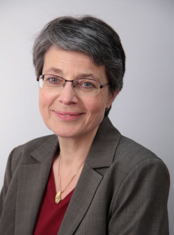
Sustaining Innovation in Europe: The new Eureka Cluster Xecs operated by Aeneas
  Nadja Rohrbach, Xecs Programme Director, AENEAS
Sustaining Innovation in Europe: The new Eureka Cluster Xecs operated by Aeneas
Nadja Rohrbach

Nadja Rohrbach
Xecs Programme Director
AENEAS

Nadja Rohrbach

Abstract
The industry lead Cluster Xecs supports RD&I projects in the field of Electronic Components and Systems (ECS) along the whole value chain and follows the ECS Strategic Research and Innovation Agenda. It is a Eureka Cluster managed by the industry association Aeneas. The bottom-up approach enables project participants to build their consortium the way it is needed for the project, its scope and size.Xecs projects are funded at national level: currently 19 countries provide budget for projects. And articipants from any other countries can join the project if they secure the financing.The Xecs Cluster offers a supportive mentoring and coaching from preparation of the project till completion. Due to the detailed feedback given by industrial experts and public authorities project proposals can be improved and the chances for a successful completion are much higher. Participating in a Xecs Cluster project will bring added value to all type of project partners i.e. SMEs, Large Enterprises and Research and Technology Organisations and universities. It gives access to a pool of expertise, to leading-edge technology, and also to new markets.The main deadlines for the first call will be 25th February 2022 to submit the project outline and 27th May 2022 for the full project proposal.The Xecs office is here to help and guide applicants through the application process.Aeneas, operating Xecs, is an industry association promoting RD&I in Electronic Components & Systems to strengthen European competitiveness. It has currently more than 440 members and is open to new membership applications.More on Xecs: https://eureka-xecs.com/More on AENEAS: https://aeneas-office.org/

Biography
With an academic background in biology and immunology, I spent several years as a scientific officer for a member of the German Federal Parliament. Subsequently I joined the DLR Project Management Agency, initially focusing on Eureka and network projects, before becoming head of the Eurostars group. Three years ago, I was seconded by the German Federal Ministry of Education and Research to the Eureka secretariat in Brussels, where I was appointed central coordinator for the new Eureka Clusters Programme and worked with various bodies to draft the first Eureka Clusters Multi-Annual and Annual Operational Plans. I started recently at AENEAS as Xecs Programme Director being in charge of the Clusters Penta and Euripides as well.