Thursday, November 18, 2021
 

Advancements in Wireless Technologies

14:30 Opening Remarks from Session Chair, Markus Pfeffer, Group Manager Contamination and Manufacturing Control, Fraunhofer IISB
14:40
The New 6G Initiative
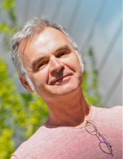
  Eric Mercier, Deputy Head of Wireless & Telecom Unit, CEA-Leti
The New 6G Initiative
Eric Mercier

Eric Mercier
Deputy Head of Wireless & Telecom Unit
CEA-Leti

Eric Mercier

Abstract
The New 6G Initiative

Biography
Eric Mercier is the deputy head of the Wireless & Telecom Unit at CEA-Leti. After having held positions in test equipment for physical fiber-optical link tests and semiconductor companies as R&D application and marketing engineer, he was promoted to managing head of the RFIC Design Laboratory. He is now in charge of promoting and disseminating scientific developments in the wireless domain, including mmW, RFID, IoT, LiFi, Radar, antenna & propagation modelling, integrated circuits, demonstration platforms and full demonstrators. He has also been involved in several European projects and has co-authored conference papers and book chapters. He is a graduate of ENSEEIH Toulouse, France.

15:00
Engineered Substrates and Materials for 5G
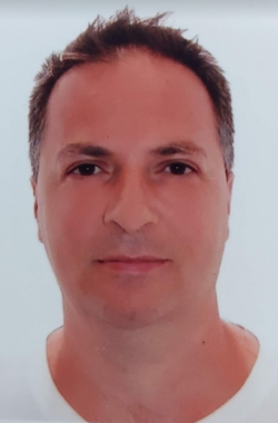
  Cesar Roda Neve, R&D Program Manager, SOITEC
Engineered Substrates and Materials for 5G
Cesar Roda Neve

Cesar Roda Neve
R&D Program Manager
SOITEC

Cesar Roda Neve

Abstract
information coming soon

Biography
Cesar Roda Neve was born in Madrid, Spain, in 1975. He received the Msc. Engineer degree from the ICAI Universidad Pontificia de Comillas, Madrid, Spain, in 2000. In 2012, he received the Ph.D. degree in engineering sciences from the Université catholique de Louvain (UCL), Belgium. From 2004 to 2006, he was with the Electronics Department of the University Carlos III of Madrid, Spain, where he worked on ROF links and optoelectronic devices. From 2006 to 2012, he joined the Microwave Laboratory at the Université catholique de Louvain (UCL), Belgium, where he worked on the characterization and application of Si-based substrates for RF integration, in particular the use of HR-Si, HRSOI, and trap-rich HR-SOI substrates, non-linearities and parasitic effects. From 2013 to 2016, he was with the 3D and Optical Technology group at IMEC, where he worked on signal integrity, power delivery networks and RF modeling with special attention to 3D stacking and packaging. From 2016 to 2020, he worked at M3Systems Belgium as project manager for GPS, interferences and satellite related projects. In 2021 he joined SOITEC Belgium as R&D Program Manager. His research interest are new applications for SOI substrates for RF, with focus in 5G and 6G communications.

15:20 5G Application and use cases, Dr.-Ing. Dr.-Ing. habil. Ivan Ndip, Fraunhofer IZM
15:40
Opportunities and challenges of high-throughput 3D metrology equipment for semiconductor process control
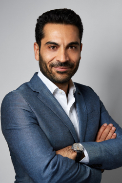
  Hamed Sadeghian, CEO, Nearfield Instruments
Opportunities and challenges of high-throughput 3D metrology equipment for semiconductor process control
Hamed Sadeghian

Hamed Sadeghian
CEO
Nearfield Instruments

Hamed Sadeghian

Abstract
In the semiconductor industry, Moore's law comes with increasing and complex demands and the need for advanced process control metrology. Traditional metrologies like OCD or CD-SEM lose sensitivity due to diminishing interaction volume. A metrology technique that thrives in this regime is Atomic Force Microscopy (AFM).AFM is a technique currently used in process and integration development because it can provide reference-level local imaging and metrology. Unique strength over competing metrology techniques includes the potential for undistorted, local high-resolution information. Two factors are currently limiting deployment of AFM tools for inline process control: 1) ability to fully resolve deep, narrow structures and 2) throughput compatible with other metrologies currently deployed in High Volume Manufacturing (HVM). Here, we discuss the advantages of a multi-head AFM system with miniaturized high-speed AFMs working in parallel. In addition, we extend traditional AFM techniques to selective imaging and metrology of subsurface 3D structures and show a path to enabling Overlay metrology through opaque hard mask layers.

Biography
Dr. Hamed SadeghianCo-Founder, President and CEO of Nearfield InstrumentsHamed Sadeghian received his PhD (Cum Laude) in 2010 from Delft University of Technology. Four years later he received an MBA degree from the Vlerick Business School in Belgium. He is the founder (2001) of Jahesh Poulad Co., a manufacturer of mechanical equipment.Hamed worked as a system architect and leaded a team of thirty researchers in nano-optomechatronics instrumentation at TNO in Delft from 2011 to 2018. In 2016 he co-founded Nearfield Instruments and is currently president & chief technology officer at this scale-up that recently sold its first metrology instrument to a high-end chip manufacturer.Hamed Sadeghian is a part time associate Professor at the Technical University of Eindhoven. He holds more than 70 patents, and published over 100 peer-reviewed technical papers. He is currently also a principal scientist and Kruyt member of TNO.

16:00
Driving Down Cost of Ownership – New High Throughput “Cluster” Evaporation Production Tools for Wireless Applications
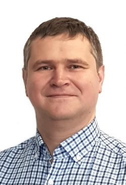
  Fiodar Kurdzesau, Process Engineer, Semiconductor Business Unit, Evatec
Driving Down Cost of Ownership – New High Throughput “Cluster” Evaporation Production Tools for Wireless Applications
Fiodar Kurdzesau

Fiodar Kurdzesau
Process Engineer, Semiconductor Business Unit
Evatec

Fiodar Kurdzesau

Abstract
Evaporation remains a powerful, flexible production technology for metallization and “lift off” process in wireless communication applications. However, manual wafer loading and the long conditioning, pumping/venting time characteristic of classical evaporation tools can make it difficult to achieve the increasingly demanding throughput and cost of ownership targets for emerging high-volume production businesses. Evatec’s innovative cluster design raises the performance bar allowing manufacturers to overcome that challenge. It combines automatic atmosphere loading with fast pumping/venting in loadlock, where a single robot for substrate handling serving up to four process chambers each equipped with its own loadlock module. The presentation will demonstrate the operation of a first BAK cluster evaporation production tool, discuss its performance, throughput and relative cost of ownership.

Biography
Fiodar Kurdzesau is Dipl. Engineer-Physicist (Gomel State University, 1999) with a PhD in Physics (EPFL Lausanne, 2009) and Technical Science (Belarussian National Academy of Sciences, 2004). Since completing his studies he has worked as a scientist within various academic Institutions (ETH Zurich, EPFL Lausanne, PSI Villigen) and within industry including Oerlikon Solar 2009-2012. He joining Evatec in 2019. His fields of interests include physics, electronics and material science with special focus on thin film deposition technology for microelectronics.