| Thursday, November 18, 2021 | |
Advancements in Wireless Technologies |
|
| 14:30 | Welcome note |
| 14:40 | Frugal Artificial Intelligence For Edge Devices |
Thomas Signamarcheix, Vice President Strategic Development, CEA-Leti Frugal Artificial Intelligence For Edge Devices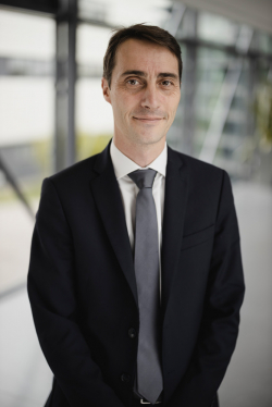
Abstract Biography |
|
| 15:00 | Engineered Substrates and Materials for 5G |
Cesar Roda Neve, R&D Program Manager, SOITEC Engineered Substrates and Materials for 5G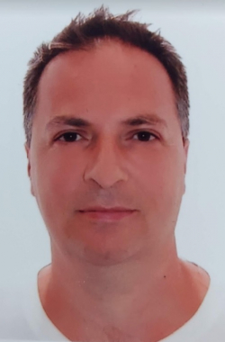
Abstract Biography |
|
| 15:20 | 5G Application and use cases, Dr.-Ing. Dr.-Ing. habil. Ivan Ndip, Fraunhofer IZM |
| 15:40 | Opportunities and challenges of high-throughput 3D metrology equipment for semiconductor process control |
Hamed Sadeghian, CEO, Nearfield Instruments Opportunities and challenges of high-throughput 3D metrology equipment for semiconductor process control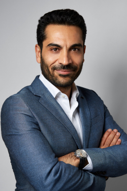
Abstract Biography |
|
| 16:00 | Sponsored presentation coming soon |