Wednesday, November 17, 2021
 

OPENING KEYNOTE

10:00 Opening remarks by Laith Altimime, President, SEMI Europe
10:10
Next Decade of Semiconductor Innovation in Europe
  Ann B. Kelleher, Senior Vice President and General Manager of Technology Development, Intel Corp.
Next Decade of Semiconductor Innovation in Europe
Ann B. Kelleher

Ann B. Kelleher
Senior Vice President and General Manager of Technology Development
Intel Corp.

Ann B. Kelleher

Abstract
coming soon

Biography
Dr. Ann B. Kelleher is senior vice president and general manager of Technology Development at Intel Corporation. She is responsible for the research, development and deployment of next-generation silicon logic, packaging and test technologies that power the future of Intel’s innovation.Previously, Kelleher was general manager of Manufacturing and Operations, where she oversaw Intel’s worldwide manufacturing operations including Fab Sort Manufacturing, Assembly Test Manufacturing and strategic planning, as well as corporate quality assurance and corporate services. Before that, she served as co-general manager of the Technology and Manufacturing Group.Kelleher joined Intel in 1996 as a process engineer, going on to manage technology transfers and factory ramp-ups in a variety of positions spanning 200mm and 300mm technologies. She started her manufacturing leadership journey as the factory manager of Fab 24 in Leixlip, Ireland. She has also been the site manager of Intel’s Fab 11X fabrication facility in Rio Rancho, New Mexico, and plant manager of Intel’s Fab 12 facility in Chandler, Arizona. She then became general manager of the Fab Sort Manufacturing organization where she was responsible for all aspects of Intel’s high-volume silicon manufacturing.Kelleher holds a bachelor’s degree, a master’s degree and a Ph.D. in electrical engineering, all from University College Cork in Ireland.


SESSION 1: IMAGINING THE NEW NORMAL

10:30 Opening remarks by session chair, Mario von Podewils, Site Manager Itzehoe, X-FAB
10:35
Market Updates
  Lita Shon-Roy, President/CEO and Founder, TECHCET
Market Updates
Lita Shon-Roy

Lita Shon-Roy
President/CEO and Founder
TECHCET

Lita Shon-Roy

Abstract
Coming Soon

Biography
Lita Shon-Roy – President/CEO and Founder of TECHCET—has worked throughout the semiconductor supply chain, leading strategy, business development, marketing and sales for chip designers, equipment OEMs, and material suppliers for over 30 years. Her experience spans from process development of SRAMs to business development of gases & precursors. She developed new business opportunities for companies such as RASIRC/Matheson Gases, Air Products & Chemicals, and IPEC/Speedfam, and managed marketing and sales in companies such as Air Products/Schumacher, Brooktree/Rockwell, and Hughes Aircraft. Ms. Shon-Roy is considered one of the leading experts in electronic materials market analysis and business development. She has authored and co-authored 100’s of articles, reports and texts on semiconductor process materials markets, trends, and worldwide supply chain issues. She holds an M.B.A. from California State University, Dominguez Hills, a M.S.E.E. focused on Solid State Physics from the University of Southern California, and a B.S. in Chemical Engineering from UC San Diego.

10:55
A Changing Market for Semiconductors
  Ondrej Burkacky, Senior Partner, McKinsey & Company, Inc.
A Changing Market for Semiconductors
Ondrej Burkacky

Ondrej Burkacky
Senior Partner
McKinsey & Company, Inc.

Ondrej Burkacky

Abstract
The semiconductor shortage is a omnipresent topic across almost all industrial verticals. We will explore several root causes for the shortage and discuss how and when they could be removed. We will look into initiatives players take to deal with the shortage.

Biography
Ondrej Burkacky is a Senior Partner in McKinsey’s Munich office. He leads globally McKinsey’s semiconductor sector and serves players across the semiconductor value chain. His functional focus is on strategy, operations and R&D.

11:15
Coronavirus, Chip Boom, and Supply Shortage: The New Normal for Global Semiconductor Manufacturing
  Stephen Rothrock, Founder, President & CEO, ATREG, Inc.
Coronavirus, Chip Boom, and Supply Shortage: The New Normal for Global Semiconductor Manufacturing
Stephen Rothrock

Stephen Rothrock
Founder, President & CEO
ATREG, Inc.

Stephen Rothrock

Abstract
Over the past 50 years, the semiconductor industry has faced its fair share of difficult challenges. The COVID-19 pandemic the world is currently experiencing has caused the worst downturn since the financial crisis of 2008, devastating global economies. And yet, the semiconductor industry has repeatedly shown incredible resilience in the face of adversity. Despite the pandemic, the market has not experienced such a dramatic upturn since 2003 and as a result, the new market upturn breaks open the fundamental flaws and risks of manufacturing concentration and outsourcing.At a time when the world is precariously dependent on Taiwan for semiconductors, how can the global supply chain forecast, manage, and plan for such sudden shifts in the future? Now more than ever before, advanced technology companies need to keep the finger on the pulse of supply and demand to successfully inform their strategic manufacturing decisions and remain agile to ensure continuity of supply. As chip demand booms in the midst of a supply shortage over the coming months and supply is no longer a given, what does the future hold for manufacturing fabs? Will greenfield become the rule rather than the exception in this new normal (TSMC in Arizona, Cree in New York, etc.)? How will the market upturn impact global fab location choices?Reflecting on some 20 years of experience completing international semiconductor manufacturing asset transactions in North America, Europe, and Asia, ATREG Founder, President, and CEO Stephen M. Rothrock will provide insights into the current global manufacturing asset market and how it is likely to evolve as part of the current market upturn.

Biography
Stephen founded ATREG in 2000 to help global advanced technology companies divest and acquire infrastructure-rich manufacturing assets, including wafer fabs (front- and back-end) as well as MEMS, solar, display, and R&D facilities. Over the last 22 years, his firm has completed 40% of all global operational wafer fab sales in the semiconductor industry, a total of 100 transactions representing a value of over $6 billion.Recent global acquisitions and dispositions have involved Allegro MicroSystems, Texas Instruments, VIS, Micron, NXP, onsemi, Fujitsu, GlobalFoundries, Renesas, IBM, Infineon, Maxim, Sony, and Qualcomm to name just a few. Prior to founding ATREG, Stephen established Colliers International’s Global Corporate Services initiative and headed the company’s U.S. division based in Seattle, Wash.Before that, he worked as Director for Savills International commercial real estate brokerage in London, UK, also serving on the UK-listed property company’s international board. He also spent four years near Paris, France working for an international NGO. Stephen holds an MA degree in Political Theology from the University of Hull, UK and a BA degree in Business Commerce from the University of Washington in Seattle, USA.

11:35
Success Stories of Digital Transformation: The ASML Case
  Steven Steen, Director, Product Management - 3D Memory Solutions, ASML
Success Stories of Digital Transformation: The ASML Case
Steven Steen

Steven Steen
Director, Product Management - 3D Memory Solutions
ASML

Steven Steen

Abstract
Coming soon

Biography
Steven Steen is director of Product Management at ASML. In this role he is responsible for the applications to drive overlay performance of ASML’s scanners. After his education at the Hogeschool Enschede he already started his career at IBM’s T.J. Watson Research Center during the final stages of his education.Leading edge innovation is the consistent thread during his 24 years’ experience in semiconductor R&D (of which 20 in lithography). Steven joined IBM Research in 1997 to develop and commercialize full chip timing diagnostics through Picosecond Imaging Circuit Analysis. In 2001, Steven moved to the chip processing side by joining the Microelectronics Research Line at IBM Research and started his lithography career there. During a wide variety of roles he worked to realize numerous device technologies and business opportunities. He moved to the Netherlands and joined ASML in 2012 to lead the definition and development of innovations and unique product offerings to ASML’s customers.Holder of over 22 US Patents and 35 published research papers, Steven continues to think of new applications and the challenges of the future. Outside of work he is often found near the water for sailing, swimming or other forms of water sports.

11:55 Panel discussion

Panel Discussion

Moderation Ondrej Burkacky, McKinsey & Company, Inc.

Ondrej Burkacky

McKinsey & Company, Inc.

Panelists
  • Lita Shon-Roy, President/CEO and Founder, TECHCET
  • Lita Shon-Roy

    Lita Shon-Roy
    President/CEO and Founder
    TECHCET

    Lita Shon-Roy

    Biography
    Lita Shon-Roy – President/CEO and Founder of TECHCET—has worked throughout the semiconductor supply chain, leading strategy, business development, marketing and sales for chip designers, equipment OEMs, and material suppliers for over 30 years. Her experience spans from process development of SRAMs to business development of gases & precursors. She developed new business opportunities for companies such as RASIRC/Matheson Gases, Air Products & Chemicals, and IPEC/Speedfam, and managed marketing and sales in companies such as Air Products/Schumacher, Brooktree/Rockwell, and Hughes Aircraft. Ms. Shon-Roy is considered one of the leading experts in electronic materials market analysis and business development. She has authored and co-authored 100’s of articles, reports and texts on semiconductor process materials markets, trends, and worldwide supply chain issues. She holds an M.B.A. from California State University, Dominguez Hills, a M.S.E.E. focused on Solid State Physics from the University of Southern California, and a B.S. in Chemical Engineering from UC San Diego.

  • Stephen Rothrock, Founder, President & CEO, ATREG, Inc.
  • Stephen Rothrock

    Stephen Rothrock
    Founder, President & CEO
    ATREG, Inc.

    Stephen Rothrock

    Biography
    Stephen founded ATREG in 2000 to help global advanced technology companies divest and acquire infrastructure-rich manufacturing assets, including wafer fabs (front- and back-end) as well as MEMS, solar, display, and R&D facilities. Over the last 22 years, his firm has completed 40% of all global operational wafer fab sales in the semiconductor industry, a total of 100 transactions representing a value of over $6 billion.Recent global acquisitions and dispositions have involved Allegro MicroSystems, Texas Instruments, VIS, Micron, NXP, onsemi, Fujitsu, GlobalFoundries, Renesas, IBM, Infineon, Maxim, Sony, and Qualcomm to name just a few. Prior to founding ATREG, Stephen established Colliers International’s Global Corporate Services initiative and headed the company’s U.S. division based in Seattle, Wash.Before that, he worked as Director for Savills International commercial real estate brokerage in London, UK, also serving on the UK-listed property company’s international board. He also spent four years near Paris, France working for an international NGO. Stephen holds an MA degree in Political Theology from the University of Hull, UK and a BA degree in Business Commerce from the University of Washington in Seattle, USA.

  • Steven Steen, Director, Product Management - 3D Memory Solutions, ASML
  • Steven Steen

    Steven Steen
    Director, Product Management - 3D Memory Solutions
    ASML

    Steven Steen

    Biography
    Steven Steen is director of Product Management at ASML. In this role he is responsible for the applications to drive overlay performance of ASML’s scanners. After his education at the Hogeschool Enschede he already started his career at IBM’s T.J. Watson Research Center during the final stages of his education.Leading edge innovation is the consistent thread during his 24 years’ experience in semiconductor R&D (of which 20 in lithography). Steven joined IBM Research in 1997 to develop and commercialize full chip timing diagnostics through Picosecond Imaging Circuit Analysis. In 2001, Steven moved to the chip processing side by joining the Microelectronics Research Line at IBM Research and started his lithography career there. During a wide variety of roles he worked to realize numerous device technologies and business opportunities. He moved to the Netherlands and joined ASML in 2012 to lead the definition and development of innovations and unique product offerings to ASML’s customers.Holder of over 22 US Patents and 35 published research papers, Steven continues to think of new applications and the challenges of the future. Outside of work he is often found near the water for sailing, swimming or other forms of water sports.

  • Stefan Kester, Director Sales & Marketing Vertical Market HighTech, DB Schenker
  • Stefan Kester

    Stefan Kester
    Director Sales & Marketing Vertical Market HighTech
    DB Schenker

    Stefan Kester

    Biography
    Biography coming soon

12:25

Lunch break


SESSION 2: SUSTAINABLE MANUFACTURING SOLUTIONS

13:15 Opening remarks by Joerg Recklies, Senior VP, Infineon Technologies
13:20
We create technology for a sustainable world, in a sustainable way – Our commitment to be Carbon neutral
  Alessandro Beretta, Facilities Director, STMicroelectronics
We create technology for a sustainable world, in a sustainable way – Our commitment to be Carbon neutral
Alessandro Beretta

Alessandro Beretta
Facilities Director
STMicroelectronics

Alessandro Beretta

Abstract
At ST, we create technology for a sustainable world, in a sustainable way.It is not new. Sustainability has been engraved in our business model and culture for 25 years. Our innovative technologies play a key role in enabling our customers to contribute to overcome global environmental and social challenges. And today, we are accelerating sustainability together (i.e., with suppliers, customers, employees, shareholders etc.).ST is stepping up its ambition and plans for the sustainability of its operations.We will become carbon neutral by 2027, for the 40th anniversary of ST’s creation.We have built a comprehensive program with very ambitious targets for a company with such a large, global manufacturing footprint, and we are working with key partners and stakeholders in a collaborative approach.

Biography
Alessandro Beretta is Facilities Director, at STMicroelectronics. After degree in Chemical Engineering at Politecnico di Milano (Italy), he worked in the Oil and Gas sector as process engineer.He joined STMicroelectronics in 2004 and he worked as Facilities Engineer and Facilities Manager, following different 200mm extension projects in Agrate, with different corporate assignment in facilities and environmental programs.Today is involved as MEP (Mechanical Electrical Process) manager in the construction of a new 300mm semiconductor FAB in Agrate (Italy) and he is worldwide project leader for the direct emission reduction workstream (Scope 1), part of the 2027 ST Carbon Neutrality program.

13:40
Broader view of sustainability challenges for a subfab in Europe
  Chris Jones, Environmental Solutions Business Development Manager, Edwards
Broader view of sustainability challenges for a subfab in Europe
Chris Jones

Chris Jones
Environmental Solutions Business Development Manager
Edwards

Chris Jones

Abstract
Energy, water, waste, climate change, pollution are repeated themes in many corporate sustainability reports. The EU’s Green Deal sustainability roadmap shows how climate neutrality and sustainability can fuel economic growth. In this paper we discuss how to meet some of the sustainability challenges encountered during the operation of vacuum and abatement on semiconductor equipment.

Biography
Chris Jones is a Ph.D. qualified chemist and has extensive experience in developing methods to help manage environmental compliance within the semiconductor, nuclear, military, and pharmaceutical industrial sectors, and is looking to communicate the importance sustainability to process developers, tool designers, and factory operators. We all need to have some understanding of how we integrate equipment into a fab to ensure that we have a profitable, safe, and environmental compliant facility. He is the Environmental Solutions Business Development Manager within the Edwards Organisation.

13:55
Mental Ill Health – The other invisible threat
  Caroline Gierczynski, Senior Manager, Field Service SHE, Edwards Vacuum
Mental Ill Health – The other invisible threat
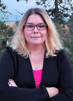
Caroline Gierczynski

Caroline Gierczynski
Senior Manager, Field Service SHE
Edwards Vacuum

Caroline Gierczynski

Abstract
The subfab is a high pressure environment and continues to present significant hazards to the semiconductor workforce. Hazards such as toxic chemicals, radiation and high voltage are commonplace and, in general, well controlled. But are there unidentified hazards which can cause workers to take time off, quit and be less effective at work even to the point they could contribute to workplace accidents? And did COVID-19 bring more into the workplace than just a biological hazard?Using examples from Edwards’ experience and our journey so far, this abstract will explore the hidden problem of Mental Ill Health, what can be done to unearth it, causes of work-related stress, and, most crucially, what we can do to improve things so employees are happy, present at work (in mind and body) and working at their best.

Biography
Caroline Gierczynski is Engineer for Safety, Health, Environment and Quality in the Edwards Vacuum Semiconductor EMEA Customer Center. She holds an Engineering degree in Chemistry and has held various positions in production and project management in semiconductor companies before joining Edwards Vacuum in 2012. She worked initially on projects to improve product quality. Later, she increased her scope of work by adding SHE to her Quality role. She is a certified instructor of i-Act and holds General Certificate in Occupation Health and Safety from the National Examination Board in Occupational Safety and Health (NEBOSH).

14:10
An Emerging Process Technology for Europe
  Reinhart Richter, President, EBARA Precision Machinery Europe GmbH
An Emerging Process Technology for Europe
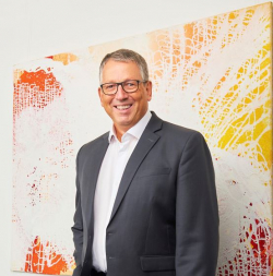
Reinhart Richter

Reinhart Richter
President
EBARA Precision Machinery Europe GmbH

Reinhart Richter

Abstract
Key topics:Performance - Customer Orientation - SustainabilityGet more out of it - added value for fabs and sub fabsEdge control - many challenges to tackleEnhance wafer yield with high quality bevel polishingNew strategic end marketsAdvanced cleaning

Biography
Dr Reinhart Richter is serving as President of EBARA Precision Machinery Europe GmbH since 2015. EBARA is a supplier for CMP and plating equipment as well as vacuum pumps and abatement systems.Prior to EBARA Reinhart has worked for over 13 years at Multitest as vice president sales and marketing and later president successfully promoting the company’s transition to a leading edge solution supplier for advanced test handlers, test sockets and DUT boards. After the acquisition of Multitest by LTX-Credence he served the newly formed Xcerra Corp. as chief technology officer. Before joining Multitest he held various positions at KLA-Tencor Corp., BBN Inc., and IABG.Reinhart Richter holds a M.Sc. and Ph.D. in Solid State Physics from McGill University, Montreal, Canada, and has authored over a dozen peer reviewed scientific papers.From 2014 to 2017 Reinhart has served on the SEMICON Advanced Packaging and Test Conference Committee.

14:30
How Can a Supplier Help Its Semiconductor Customers to Fight against the Supply Chain Crisis in Time of Covid ?
  Yutao Huang, Helium Director, Air Liquide
How Can a Supplier Help Its Semiconductor Customers to Fight against the Supply Chain Crisis in Time of Covid ?
Yutao Huang

Yutao Huang
Helium Director
Air Liquide

Yutao Huang

Abstract
Coming soon

Biography
Coming soon

14:50 Coffee break
 

SESSION 3: FAB AUTOMATION: PROCESS & EQUIPMENT TRANSFORMATION FOR A CONNECTED, INTELLIGENT FAB

15:15 Opening Remarks by Session Chair, Dr. Susan Weiher, VP Engineering Operations, OSRAM Opto Semiconductors GmbH
15:20
Reduced time to production after equipment delivery
  Thomas Gebhardt, Manager Technical Sales, Ap-s
Reduced time to production after equipment delivery
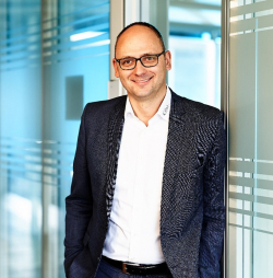
Thomas Gebhardt

Thomas Gebhardt
Manager Technical Sales
Ap-s

Thomas Gebhardt

Abstract
In current times with shortages of semiconductors, ramp-up of production capacities becomes globally more important than in former times. AP&S implemented an in-house facility and strategy to significantly reduce leaching times of new installed wet process equipment and thus speed-up the availability for production. Efficient rinsing of every equipment by ultra-high-purity water ensures a reliable cleanliness and quality of the equipments before shipment. Quality monitoring before delivery is done by optical laser counters and different analytics. Benefits of this strategy for our customers will be part of the presentation.

Biography
Thomas Gebhardt started in 2019 at AP&S as Manager Technical Sales. He began his career in the semiconductor industry already in 1999, more than 20 years ago, as a technical support engineer. He is located at the AP&S subsidiary in Dresden which can be described as Semiconductor Heart of Germany. From there, he supports local customers as well as customers in the UK, Scandinavia and Russia.

15:30
Smart to the Rescue!
  John Behnke, GM Final Phase Systems, INFICON
Smart to the Rescue!
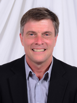
John Behnke

John Behnke
GM Final Phase Systems
INFICON

John Behnke

Abstract
The semiconductor industry and its supply chain struggle have made the global news almost daily in 2021. This has led many countries to create Semi specific investment initiatives to improve their domestic production of chips to better control their supply chain. These efforts include funding proposals for new regional fabs as well as improving existing production capabilities. This presentation will not comment on the political motivations of these efforts but will instead focus on the criticality of Smart Manufacturing solutions to these efforts. Whether getting more capacity out of existing fabs, enabling fabs run a broader mix of technologies and products for a longer period or to ensure a new site is built with tomorrow’s technology instead of yesterday’s Smart Manufacturing is key. We will review the elements of Smart Manufacturing that can be rapidly deployed in an existing fab to deliver high ROI through improvements in output and cycle time. These initial key elements are intended to require few fab resources to deploy since they are spread thin today. Quickly establishing these capabilities can help maintain a company’s historical supply reputation during these high demand times. Follow on additional Smart Solutions can be added to further improve existing fabs. Green Field new fabs offer more opportunities to leverage Smart solutions but will not deliver significant output for years due to the time required to build. A “Must Have” list of existing and in development Smart solutions for these fabs will also be reviewed.

Biography
Mr. Behnke has 35 years of semiconductor industry experience including: logic and memory manufacturing, technology/product development and fab operational excellence. As the GM of Final Phase Systems an INFICON Product Line, John leads a team that develop and deploy SMART software solutions that enable fabs to improve their manufacturing efficiency. FPS’s suite of software solutions are built upon a common Datawarehouse which enables advanced Fab Scheduling and optimized WIP movement as well as other related capabilities. He is also a Co-Chair of the Semi North America Smart Manufacturing Special Interest Group. Prior to FPS John served as the CEO and President of Novati Technologies, the SVP and GM of the Semiconductor Group of Intermolecular, the CVP for Front End Manufacturing, Process R&D and Technology Transfers at Spansion and the Director of AMD’s Fab 25’s Engineering and Operations groups where he was a founding member of AMD’s Automated Precision Manufacturing (APM) initiative which led the Semiconductor industry’s development and use of APC and other advanced factory systems. He also led the successful conversion of Fab 25 from Logic to Flash memory which was enabled through the virtual automation of the fab.Mr. Behnke earned a B.S. degree in Mechanical Engineering with an Industrial Engineering Minor from Marquette University. Mr. Behnke holds five U.S. patents.

15:50
How to Replace Conventional Wet Etch/Clean Tools with Batchspray® Equipment, While Reducing Chemical Costs and Achiving More Clean Room Space?
  David Neunteufel, Global Account Manager, Siconnex customized solutions GmbH
How to Replace Conventional Wet Etch/Clean Tools with Batchspray® Equipment, While Reducing Chemical Costs and Achiving More Clean Room Space?
David Neunteufel

David Neunteufel
Global Account Manager
Siconnex customized solutions GmbH

David Neunteufel

Abstract
A case study, that was done together with a customer, shows the benefits of moving from conventional wet etch/clean tools to a BATCHSPRAY® equipment.Due to that change the customer generated clean room space and reduced the chemical consumption to a minimum.These benefits were also achieved by a new wafer handling system for automated BATCHSPRAY® equipment. It is called Retainer Comb Handling system (RCH).That system allows a huge open area on the wafer surface by which a good chemical exchange is given.This means high cost savings as well as a good return on invest.

Biography
David Neunteufel started as Service Engineer at Siconnex in 2012, supporting customers around the globe in any service topic. After about 4 years of technical experience as Service Engineer, he moved to the Technical Sales Support. In this position he focused on cost of ownership & return on invest calculations. He became Global Account Manager in 2017 and handles several international accounts.

16:10
Can AI Optimize Your Equipment's Throughput ?
  Mike Barrett, Director of Global OEM Sales, PEER Group
Can AI Optimize Your Equipment's Throughput ?
Mike Barrett

Mike Barrett
Director of Global OEM Sales
PEER Group

Mike Barrett

Abstract
In response to global chip shortages, many semiconductor fabs have started to demand even higher throughput from the equipment on their manufacturing floors. While process timing is often constrained by physics, opportunities do exist to reduce wait time waste by optimizing the manner in which substrates are scheduled within complex tools, for example, in equipment that combines multiple operations within a single cluster.However, scheduling wafer flows within a complex cluster tool – particularly in a high-volume, high-mix environment – presents several engineering challenges for optimizing wafer movements. Is it possible to avoid deadlocks and maximize throughput while enforcing strict process and recipe rules? When a tool’s components are operating in a degraded mode or are disabled for maintenance, can the equipment continue to perform efficiently? A tight labor market that requires OEMs to make tough decisions about where to allocate scarce expert developers compounds the challenge.Advances in artificial intelligence (AI) and machine learning have introduced the possibility for automated solutions that can discover optimal routing in real time, replacing the effort for creating high-quality substrate schedulers manually. Such an approach would increase fab throughput while simultaneously reducing time to market and engineering effort for OEMs.In this talk, PEER Group will compare three generations of cluster tool schedulers: Traditional, Offline optimized via machine learning, and Real-time equipment optimization using AI.

Biography
Mike Barrett is the Director of Global OEM Sales at The PEER Group Inc., the largest supplier of factory automation software for semiconductor OEMs and factories. He and his global team ensure PEER Group provides software solutions that meet every OEM customer’s unique needs. Mike came to PEER Group with a strong background in software automation, having worked in a variety of engineering and software development roles. He holds an Honours Bachelor of Applied Science in Computer Engineering from the University of Waterloo and is a licensed professional engineer in the province of Ontario.

16:30
Supporting Europe’s Semiconductor Expansion Through Localised Training and Service
  Joerg Arnold, Parts and Service Sales Executive, Tokyo Electron Europe Limited
Supporting Europe’s Semiconductor Expansion Through Localised Training and Service
Joerg Arnold

Joerg Arnold
Parts and Service Sales Executive
Tokyo Electron Europe Limited

Joerg Arnold

Abstract
The operational changes brought about by the pandemic have greatly impacted the semiconductor industry due to the increases in localised installation, service, and support. Localising these areas presents several key challenges due to the complexity and high precision of semiconductor production equipment. It is further complicated by the impending aggressive growth of semiconductor production due to the global semiconductor chip shortage. Given these restrictions, how does a global company like Tokyo Electron (TEL) locally install our products, and meet the service and support needs of the European semiconductor business environment? As a reliable partner for our customers, we will share our localisation strategies to address how we are adapting to these challenges.

Biography
Jörg has already more than 15 years experience in the Semiconductors industry. Upon his graduation in Business Administration from Technische Universität (TU) in Dresden, Jörg joined the Advanced Mask Technology Center in 2004 and AMD in 2006. In 2008 he has moved on to Tokyo Electron, serving in different roles within the Service and Support Department. In 2019 he was appointed as Service and Parts Sales Executive.Jörg works closely with the TEL Field Solution Business Unit implementing global projects for service and parts into Europe.

16:40
Enabling smart fabs with next-generation production scheduling
  Jamie Potter, CEO & Co-founder, Flexciton
Enabling smart fabs with next-generation production scheduling
Jamie Potter

Jamie Potter
CEO & Co-founder
Flexciton

Jamie Potter

Abstract
Coming soon

Biography
Jamie is an expert in Mathematics and Statistics and graduated top of his year from the University of Oxford. In 2018, Jamie was added to the 2018 Forbes 30 under 30 list.

17:00
Remote Operations / Training New Employees in Time of Disruption; Integrating New Training Solutions; Managing Operations when Staff is Digital.
  Andreas C. Zimmer, Executive Search & Selection Consultant, ZIAN & Co industrial consulting and recruitment
Remote Operations / Training New Employees in Time of Disruption; Integrating New Training Solutions; Managing Operations when Staff is Digital.
Andreas C. Zimmer

Andreas C. Zimmer
Executive Search & Selection Consultant
ZIAN & Co industrial consulting and recruitment

Andreas C. Zimmer

Abstract
CoViD has proven one thing: it is possible to run a company successfully without the physical presence of employees! What does this mean for the future? Will home office establish itself? What impact will this have on management and onboarding of new employees? How do I lead a digital team? It will depend on some factors to be used differently. In detail:Team building: lead teams horizontally. One success factor is that everyone is deployed according to their skills, meaning not only their professional qualifications, but also their skills in terms of ​​interpersonal relationships. The team leader will be well advised to select his team members from this aspect and deploy them accordingly. He is therefore not necessarily the most senior, but rather the one who is most likely to be able to organize, lead and motivate the team and enable them to focus on the task at hand: he's the coach on the sideline, not the best player.Communication: communicate openly, honestly and at an early stage. It is more about “listening” than “talking”, as a remote team will only be successful if all members have the same information and know exactly what is expected. Criticism is expressly encouraged, and suggestions should come from those who deal with the topic every day. “Leading through questions” should prevail.Clear goals, tasks, responsibilities: a precise distribution of tasks is essential. It will be important that those who are best qualified for the respective task take on responsibility, and this qualification is not necessarily a purely technical one. Likewise, it will be necessary to precisely define the goals and to adapt them, should this prove necessary. It is not a top-down process, but an iterative action that accompanies the process fluently. A framework should be set out within which the team members can move freely.Equipment, timing, schedule: ensure (as team leader) that the team has the necessary equipment available right from the start; give clear time constraints, keep an approved agenda, and stick to it.Participants (n ° of max): the team: as small as possible, as large as necessary.Develop people: give colleagues the chance to work out their ideas and suggestions; discuss these with them; give open, honest feedback; praise freely and honestly; give credit; think about each one in your final report.You'll end up successfully if you respect some simple lessons: coach your team; generate enthusiasm; develop people; ask; say “Yes, we'll do it”.

Biography
Andreas is an international acting personnel and industrial consultant with 25+ years’ experience. He’s a specialist for high-end technologies (Semi, LED, PV, Electronics, Test & Measurement, etc.), active throughout Europe, with customers in Europe, USA, Asia. He’s a permanent participant of leading exhibitions and conferences worldwide (SEMICON, INTERSOLAR, EU PV SEC, LIGHT&BUILDING, ELECTRONICA, PRODUCTRONICA) and fluent in three languages, written and spoken.Within the SEMI industry, he operates with his partners from SONAR GmbH, Munich (www.sonar-gmbh.com).Prior to his consultancy career, Andreas covered positions in Sales and Marketing with OSRAM, Germany and Italy, for almost ten years. Further on, he matured experience in controlling, change management, re-engineering. Andreas lives in Munich. He has one son and is in his spare time an avid tournament ballroom dancer and sailor.For more information, go to his LinkedIn-profile: https://www.linkedin.com/in/andreas-c-zimmer-16807112/, or contact him directly: aczimmer@zianco.com or +49 89 31988638.

17:20
Challenges and Opportunities for Adopting Digital Twins in Semiconductor Industry
  Fahad Golra, Research Coordinator, Agileo Automation
Challenges and Opportunities for Adopting Digital Twins in Semiconductor Industry
Fahad Golra

Fahad Golra
Research Coordinator
Agileo Automation

Fahad Golra

Abstract
Virtualization of a real-life object, process or system is not new; what brings the concept of digital twins to the forefront is its potential real time connection to the real world and leveraging AI and big data analytics to interact with and evaluate different “what if” scenarios.Through our experience in the development of digital twin solutions for semiconductor equipment manufacturers, we share the findings of an analysis on their adoption in semiconductor industry.Depending on their perspective, OEMS and integrators have an outgoing focus by finding its value for product improvement, customer service and new business models. On the contrary, fabs have an incoming focus by finding its value for cost reductions, process improvements and safety. By replicating manufacturing systems and processes, digital twins afford an opportunity for online and offline support for extending the APC technologies like Equipment Health Monitoring for assessing tool health as a function of deviation from normal behavior, Predictive Maintenance for using process and equipment state information to predict maintenance needs, Predictive Scheduling for improving scheduling of system by utilizing current and projected information on tool and factory state, capabilities and schedule, Virtual Metrology for the prediction of post process metrology variables using process and wafer state information, and Yield Prediction for monitoring information to predict process or end of line yield.For adopting digital twins, the stakeholders will have to prepare themselves for new challenges. The product teams need to become proficient in both hardware and software by developing new skills like design, simulation, analytics, etc. Integration, management, and maintenance of both physical and digital twins need to be considered. Maintenance of digital twins and their links to the physical twins become a core approach for upgrades and thus require new business models. An additional effort to standardize data interchange, not only between the physical and digital twins but also for the integration of digital twins would be required. With more data from digital twins, unless the stakeholders can find innovative “what if” scenarios, its value would remain unclear. The ownership of data is already becoming an important concern. The stakeholders would need to devise procedures for data sharing and partitioning and ensure the confidentiality of data and intellectual property security.

Biography
Fahad Golra is currently working as a research coordinator at Agileo Automation. After his doctorate in process modeling, he has been active in research activities around model federation, model driven development, Industry 4.0 solutions based on RAMI 4.0, OPC UA and digital twins. He is actively participating in different standardization activities in OPC Foundation, SEMI association and ISA.

17:40
Vocus: The Most Sensitive Detector of Air Molecular Contaminants
  Carla Frege, Application scientist, Tofwerk
Vocus: The Most Sensitive Detector of Air Molecular Contaminants
Carla Frege

Carla Frege
Application scientist
Tofwerk

Carla Frege

Abstract
A fast and precise monitoring of room air and material outgassing is critical to ensure good product quality in the semiconductor industry. As cost per chip rises significantly from one technology node to the next, maintaining optimal yield is more than ever paramount. As such, measurement of air molecular contaminants (AMCs) from high to extremely low concentration levels (ppmv-pptv) has become of great importance within the different fab processes. Current technologies used for monitoring AMCs are specific to some categories (acids, bases, volatile organics, condensables) and/or fail detecting low concentration levels of AMCs. The TOFWERK Vocus chemical ionization mass spectrometer offers new insights into monitoring of AMCs in the fab with extremely fast time response (seconds), detection limits in the range of single digit pptv and high versatility being able to measure trace acids, bases, condensables and volatile organic compounds simultaneously . Vocus is also a mobile instrument that can, when necessary, be deployed to specific areas within the fab. In this work we present the use of a Vocus for continuous monitoring of outgassing after a process that simulated standard cleaning procedures of a FOUP (a specialized plastic enclosure used for wafer transport). For these measurements the outgassing of molecular acids (MAs) and molecular bases (MBs) was monitored over 16 hours in separate experiments simulating cleaning of a FOUP. With 1 min LODs in the range of 3-10 pptv, Vocus measures some molecular contaminants that persist at trace concentrations (10-30 pptv) for many hours.

Get
Concentration decay of common inorganic acids in a FAB environment. The markers show the quantification limit of each compound. Arrows on the right axis show the 1 minute LOD of the Vocus
Precise and sensitive measurement of the outgassing compounds could guide process adjustments to decrease defects related to queue time and optimize the cleaning process of individual FOUPs prior to loading with new batches of wafers. More importantly, such measurements could inform development of next generation of FOUPs using novel polymeric materials and new surface treatment procedures.

Biography
Carla Frege is an application scientist at Tofwerk AG (Thun-Switzerland). She holds a PhD degree in atmospheric and climate science from the Swiss Federal Institute of Technology in Zürich (ETHZ). Her interests lie in the application of atmospheric science to industrial use-cases. Her current projects include the research and development of sensitive technology for monitoring of airborne molecular contamination (AMC) in the semiconductor industry.