,
Magnetocalorics: Next-Generation Cooling for Semiconductors

,

Abstract
Magnoric is developing a new generation of cooling systems based on the magnetocaloric effect, replacing conventional vapor-compression technology with a solid-state thermodynamic cycle.Our technology operates without refrigerant gases and combines high energy-efficiency potential with silent, vibration-free operation and reduced maintenance requirements.Magnoric has already developed and validated pre-series cooling platforms from a few hundred watts to more than 1 kW and is now scaling the technology toward higher-power applications.For the semiconductor industry, magnetocaloric cooling opens new opportunities for efficient thermal management, process cooling and heat recovery. This presentation will introduce Magnoric’s technology, its latest developments and its potential for next-generation semiconductor manufacturing applications.

Biography
Rémi Dubois is Chief Operating Officer at Magnoric, a French deep-tech company developing magnetocaloric cooling technologies. He is responsible for operations, business development and the industrialization of Magnoric’s technology, working closely with industrial partners across cooling, energy and advanced manufacturing applications.

Advanced Packing Conference
Fab Management Forum
imec ITF - Building the silicon backbone of Europe’s AI leadership
Entegris
Materials Innovations
Smart Mobility
MEMS & Imaging Sensors Summit
CxO Summit
Future Disruptions
Smart Manufacturing
Electrification and Power Semiconductors
CEA-Leti | Engineering the Semiconductor Foundations of the AI Era
Start Up Pitches
A To top
ACCRETECH GmbH ACCRETECH GmbH Ossmann, Christian
Coming Soon

Ossmann, Christian
VP & COO
ACCRETECH GmbH

Ossmann, Christian

Abstract
Coming Soon

Biography
Coming Soon

Advanced Packing Conference
Advantest America, Inc. Advantest America, Inc. Leventhal, Ira
Bridging the Gap from Prototype to Production: High-Volume Manufacturing Test and Qualification for Co-Packaged Optics

Leventhal, Ira
VP of Applied Research & Technology
Advantest America, Inc.

Leventhal, Ira

Abstract
Co-Packaged Optics (CPO) enables higher bandwidth density and lower power for AI, HPC, and next-generation data centers by placing optical engines close to advanced compute and networking devices. However, scaling CPO from prototypes to high-volume manufacturing (HVM) requires more than photonic integration and advanced packaging. The main challenge is to build a production-ready test and qualification infrastructure that can handle optical, electrical, thermal, mechanical, and operational requirements with the repeatability and throughput expected in semiconductor manufacturing. Key barriers include reliable optical connectivity at package level, insertion-loss control, polarization preservation, connector wear, contamination sensitivity, precision alignment, external laser delivery, calibration stability, thermal-mechanical integration, serviceability, and long-term reliability. These issues affect both Final Test (FT) and System-Level Test (SLT) and must be solved without compromising automation, changeover efficiency, equipment utilization, or cost of test.This paper presents a modular platform architecture to address these challenges. It extends existing semiconductor test cells with a dedicated co-packaged interface layer that supports optical routing, laser delivery, calibration, diagnostics, cleaning concepts, and photonic test integration while maintaining compatibility with current handlers, sockets, load boards, and automated test equipment. The platform approach allows different optical engine designs, connector concepts, and production test strategies — such as optical loopback, instrument-assisted characterization, and system-level qualification — to be supported without redesigning the full manufacturing cell.By combining standardized interfaces, automated calibration, contamination mitigation, serviceable optical paths, and scalable test flows, the proposed architecture provides a practical path from New Product Introduction (NPI) to HVM. It helps manufacturers manage yield, reliability, throughput, and ecosystem interoperability as CPO devices move into production for photonic-enabled AI and HPC systems.

Biography
Ira Leventhal Ira Leventhal is the Vice President of Research & Venture at Advantest America, Inc. He has over 25 years of experience in semiconductor testing, including memory, SoC, wireless device, and system-level test. Ira has led the design and development of multiple generations of ATE systems and holds 15 patents in a variety of test-related technologies. In his current role, Ira is focusing on how state-of-the-art and emerging technologies can be applied to meet the challenging test requirements driven by HPC/AI devices and advanced packaging. Ira is an SBEE graduate of the Massachusetts Institute of Technology.Preet Paul Singh is Engineering Director, Research & Ventures at Advantest America, where he leads advanced semiconductor test and measurement initiatives for next-generation semiconductor and optical interconnect technologies. Over a career spanning more than two decades, he has led the development and deployment of multiple generations of semiconductor test systems for memory, logic, and system-level test applications.His experience spans product development and leadership roles at Advantest, Verigy, Agilent Technologies, and Hewlett-Packard. His expertise includes semiconductor test system architecture, high performance compute, instrumentation, and manufacturing test solutions. He currently leads R&D activities focused on packaged silicon photonics and co-packaged optics (CPO), addressing the test challenges of next-generation AI and high-performance computing infrastructure. Preet holds a B.S. in Electrical Engineering and Computer Science from the University of California, Berkeley.

Advanced Packing Conference
Advantest Italia S.r.l Marino, Fabio
From Megawatts to Microseconds: Enabling Sustainable AI Through Power Semiconductor Innovation and Test

Marino, Fabio
Managing Director
Advantest Italia S.r.l

Abstract
Modern test systems are no longer simply production tools; they are strategic enablers of innovation. As AI reshapes the world's energy landscape, Advantest power test solutions help unlock next-generation power semiconductors full potential by ensuring uncompromising efficiency, reliability, and performance.

Biography
MARINO FABIOBorn in Italy in 1971. Hold a MS degree (1997) in electronics and a MBA (2012).Joined semiconductor industry in 1998 as designer and application engineer for analog and mixed signal devices. Since 2007 moved to management level with responsabilities in leading application engineer teams and account management.Joined Advantest in 2011 where currently holds the roles of MD for Advantest Italia S.r.l. and for CREA S.r.l.

Smart Mobility
AEMtec GmbH Lieske, Daniel
Advanced Packaging for high mix and low volume, Flip Chip capabilities beyond the standard in Europe

Lieske, Daniel
Senior Expert Advanced packaging
AEMtec GmbH

Abstract
This presentation will showcase AEMtec's flip chip capabilities especially developed for harsh environments like applications in space. It will give first reliability results and processes, that have been used for qualification purpose under the support of ESA (European Space agency). Furthermore we will show the demand in future for FOWLP, Copper pillar and micro bump in the field of flip chip and chiplet applications.Discover how AEMtec transformed from an IDM into a leading specialized OSAT, carving out a unique position in the European semiconductor landscape. While industry roadpaths often follow rigid lines, AEMtec thrives on complexity: we build custom-specific package designs that lay the groundwork for future technologies.

Biography
Daniel Lieske, Senior Expert Advanced Packaging @ AEMtec GmbHDaniel Lieske is Senior Expert for Advanced Packaging Technologies at AEMtec in Berlin.In this role, he supports both product and process development teams and advises the sales department on new customer projects. His technical focus includes advanced packaging technologies such as Fan-Out WLP, RDL, Flip Chip, and photonics packaging, ensuring that AEMtec meets current and future market demands.He holds a diploma in Microelectronics and Microsystems from Brandenburg University of Technology in Cottbus. Daniel began his career as a Process Engineer at Infineon Technologies Dresden and Qimonda, working in the Backend on development, production, and technology transfer of multi‑chip modules to high‑volume manufacturing sites. As a Project Engineer at Freudenberg Mechatronics, he developed and optimized production equipment for automotive lighting applications.For the past 15 years at AEMtec, he has been responsible for wafer‑level solder ball attach, printing technologies, solder reflow, and failure analysis.

Advanced Packing Conference
Agate Sensors Agate Sensors Liapis, Andreas C.
Chip-scale, Software-Defined Hyperspectral Intelligence

Liapis, Andreas C.
CTO
Agate Sensors

Liapis, Andreas C.

Abstract
Coming Soon

Biography
Coming Soon

MEMS & Imaging Sensors Summit
AlphaLum SA AlphaLum SA Koch, Tanja
The Optical Interface Between Human and AI: Rethinking the Power Problem for AI Eyewear.

Koch, Tanja
Chief Business Officer
AlphaLum SA

Koch, Tanja

Abstract
Every smart glasses maker is fighting the same battle: power. A display drains the battery. Running AI to understand what the user wants drains it further, typically through power-hungry cameras and inference pipelines that can't realistically stay on all day, and even when they do run continuously, low frame rates miss the fast, subtle signals that actually carry intent. Most solutions optimize one side of this equation, a more efficient display, or a lower-power sensor, but treat the other as someone else's problem. AlphaLum optimizes both, on a single optical platform.Our holographic combiner architecture delivers a step-change in display efficiency, easing the power cost of getting information in front of the eye. At the same time, our optical micromotion sensing platform reads subtle eye and skin signals directly, combining always-on operation with high temporal resolution, capturing fast micromotions continuously rather than trading one for the other, at a fraction of the power of camera-based AI interaction. The result is a combiner that cuts power on both the output and the input side of the human-AI loop, without forcing a choice between staying on and seeing enough.This talk covers why power has to be solved on both sides of the interaction, not just the display, why the combination of always-on and high temporal resolution is the precondition for genuinely useful AI interaction on the face, and what that means for how AR glasses get designed, built, and scaled toward true all-day wear.

Biography
Tanja Koch is the co-founder and Chief Business Officer of AlphaLum, a deep-tech photonics startup based in Lausanne developing next-generation optical systems for smart glasses. She brings over nine years of experience across startup founding, venture capital, and innovation strategy, with a particular focus on the AR hardware space.Before AlphaLum, Tanja served as Senior Product Manager at ams OSRAM, one of the world's leading optical semiconductor companies, where she gained direct experience bringing complex photonic and sensing technologies from R&D to market. That industry grounding, combined with her background as both a founder and a venture capitalist, gives her an unusual vantage point: she understands what it takes to build deep-tech products from the inside, and what it takes to scale and commercialize them.Tanja holds a Master of Science in Management from the Technical University of Munich (TUM) and has continued her education at Stanford University. Her academic foundation in design thinking and user-driven innovation shapes how AlphaLum approaches product development: starting from real user constraints, including power, form factor, and all-day wearability, rather than from technology capabilities alone.At AlphaLum, she leads business development, partnerships, and go-to-market strategy as the company advances its two core platforms: an ultra-efficient holographic waveguide display and an always-on optical micromotion sensing system, together forming a bidirectional interface layer between humans and AI.

MEMS & Imaging Sensors Summit
Amkor Technology Portugal Amkor Technology Portugal OToole, Eoin
Does the Most Advanced Packaging Require the Most Advanced Metrology

OToole, Eoin
R&D Director
Amkor Technology Portugal

OToole, Eoin

Abstract
The cutting edge of advanced packaging includes tens of stacked memory dies with intricate wire bond connectors as the top layer of a Package on Package solution for an application processor (for example). The application processor will likely have fine pitch micropillars for a flip chip connection to a multilayer RDL interposer. The RDL interposer can have line width and line space features down to single digit microns, requiring organic CMP processing to achieve the necessary interlayer coplanarity. The question remains as to whether the most advanced metrology solutions are required to control such an advanced process. This presentation aims to answer that question.

Biography
Eoin OToole is a the R&D director of Amkor Technology PortugalOriginally from Dublin Ireland where he obtained his primary and master degrees in material science from Trinity College Dublin.

Advanced Packing Conference
ams-OSRAM ams-OSRAM Matthias Schilz, Christof
Coming Soon

Matthias Schilz, Christof
Vice President
ams-OSRAM

Matthias Schilz, Christof

Abstract
Coming Soon

Biography
Coming Soon

Smart Manufacturing
ams OSRAM ams OSRAM Ertl, Sabine
New Collaborations, Materials & Market for Photonics

Ertl, Sabine
Senior Vice President & General Manager
ams OSRAM

Ertl, Sabine

Abstract
Coming Soon

Biography
Coming Soon

Fab Management Forum
Applied Materials Applied Materials Britz, David
Coming Soon

Britz, David
Managing Director, Strategic & Product Marketing
Applied Materials

Britz, David

Abstract
Coming Soon

Biography
Dr. David Britz leads the Strategic Marketing & New Product organization for the ICAPS business at Applied Materials. Prior to Applied, David has experience at both Fortune 100 and startup companies in strategy, business development, and product management. David has an MBA from MIT Sloan and a DPhil in Materials from the University of Oxford.

Electrification and Power Semiconductors
AP&S International GmbH Zürcher, Stefan
Hydrodynamics-Driven wet etching for scalable fabrication of high-aspect-ratio through-glass vias in glass core substrates

Zürcher, Stefan
Head of Process Technology
AP&S International GmbH

Abstract
The scalable fabrication of high-aspect-ratio through glass vias (TGV) in large-area glass core substrates remains a critical bottleneck for next-generation advanced packaging technologies. While hybrid laser–etching approaches have demonstrated fundamental feasibility, the lack of precise control over etch homogeneity, via geometry, and process scalability continues to limit their implementation in high-volume manufacturing. This work presents an integrated, simulation-driven wet processing approach that addresses these limitations by introducing hydrodynamic control within the etching stage, enabling deterministic shaping of TGV structures at wafer and panel scale.The proposed solution builds on a combined femtosecond laser modification and selective wet chemical etching process chain, in which laser-induced structural changes in the glass bulk define regions of enhanced chemical reactivity. The key innovation presented here lies in the subsequent etching process: by engineering the fluid dynamics within the etch environment, mass transport limitations are actively mitigated.Within AP&S wet processing equipment, a novel hydrodynamic design enables uniform delivery of the etching medium. This controlled flow regime enhances local reactant availability while ensuring efficient removal of reaction by-products, resulting in improved etch kinetics and uniformity. Compared to conventional immersion-based approaches, the method allows for tighter control of critical geometrical parameters, including via diameter (20–100 µm), aspect ratios exceeding 10:1, and well-defined sidewall profiles across the entire substrate.A central contribution of this work is the integration of computational fluid dynamics (CFD) into both equipment and process design. By leveraging simulation-based optimization, the hydrodynamic conditions can be pre-configured for varying substrate dimensions and layout densities without empirical iteration. This not only reduces development time but also enables rapid process transfer across different product configurations.The results demonstrate that hydrodynamically optimized wet etching represents a key enabler for translating laser-based TGV fabrication from laboratory to industrial-scale manufacturability. The presented approach establishes a pathway toward highly uniform, high-throughput, and geometry-controlled TGV formation, thereby addressing a challenge in the deployment of glass core substrates for advanced electronic systems.

Biography
Stefan Zuercher is the Head of Process Technology at AP&S and has more than 15 years of experience in the semiconductor industry. He joined AP&S in 2011 as a process engineer for wet processes (etching, cleaning, drying, electroless UBM metallization), installing and qualifying wet process equipment worldwide for over a decade.In 2014, he became the manager of the newly established AP&S DemoCenter, and in 2017 he advanced to Process Manager. In this role, he was responsible for all process-related tasks, including tool qualifications and optimization, as well as process development across AP&S equipment platforms for singlewafer, batch, and parts-cleaning applications for advanced semiconductor manufacturing.Since 2024, as Head of Process Technology, he has fully focused on delivering customer-oriented process solutions across the AP&S product portfolio and DemoLAB, as well as driving advancements in simulation engineering within the AP&S SimLAB.

Advanced Packing Conference
Arvind Consultancy Arvind Consultancy Keskar, Sanjeev
Semiconductor & Electronics Opportunities in India

Keskar, Sanjeev
CEO
Arvind Consultancy

Keskar, Sanjeev

Abstract
Coming Soon

Biography
Sanjeev Keskar is Chief Executive Officer of Arvind Consultancy. After his successful stint of 35 years in corporate world, out of which about 29 years in semiconductor industry, Mr. Keskar incorporated Arvind Consultancy, an advisory firm in the field of developing High Value-Added Eco- System for Semiconductor and Electronics Industry in India in Nov. 2020.Prior to this, Mr. Keskar was Managing Director India at Arrow Electronics for India, a leading electronic component global distribution company for five and half years. Earlier he was Managing Director Sales at PMC-Sierra for India and SEA.He was also elected Chairman of IESA (India Electronics and Semiconductor Association) for year 2013-14 and in current year he is part of Executive Council of IESA.Prior to PMC Sierra, he was Country Manager, Sales, at Freescale Semiconductor ( Motorola ) for 5 years and Country Manager, India, for AMD Far East Ltd., where he started AMD India operations as the first Country Manager and established AMD India.Mr. Keskar has also worked at National Semiconductor as Country Manager and at Max India Ltd. as Regional Manager.Mr. Keskar is Professor of Practice at IIT Roorkee. Mr. Keskar is also Executive Director at EPIC Foundation.Mr. Keskar received a master’s degree in management science in Marketing and a Bachelor’s in Electronics and Communication Engineering and Technology, from Pune University.

CxO Summit
ASE ASE Tien, Nicole
Scaling Advanced Packaging: The Wafer-to-Panel Revolution

Tien, Nicole
Senior Technical Program Manager
ASE

Tien, Nicole

Abstract
Coming Soon

Biography
Nicole Tien is a Senior Technical Program Manager at ASE Europe, where she drives advanced packaging technology development and innovation to support customer growth and ecosystem collaboration. She focuses on high-performance heterogeneous integration, including multi-die and 3D packaging solutions, enabling improved system-level performance, bandwidth, and energy efficiency. Nicole works closely with customers and industry partners to translate emerging requirements into scalable packaging solutions, supporting applications across AI, automotive, and high-performance computing. She is actively involved in advancing packaging strategies that push the limits of thermal, electrical, and mechanical performance, helping to enable next-generation semiconductor systems

Advanced Packing Conference
ATREG ATREG Rothrock, Stephen
Panelist

Rothrock, Stephen
Founder & CEO
ATREG

Rothrock, Stephen

Abstract
Panelist

Biography
Stephen Rothrock founded ATREG in 2000 to help the world’s advanced technology companies divest and acquire infrastructure-rich manufacturing assets, including semiconductor wafer fabs (front- and back-end) as well as MEMS, display, solar, and R&D facilities. Over the last 10 years, his firm has completed 70% of all global operational wafer fab sales in the semiconductor industry, with five of these involving 300mm operational fabs. Recent global acquisitions and dispositions have involved Allegro MicroSystems, Bosch, Elmos, Fujitsu, GlobalFoundries, IBM, Infineon, Japan Display Inc., Micron, Nexperia, NXP, onsemi, Plessey, Qualcomm, Renesas, Solidigm, Sony, Texas Instruments, TSI, and Vanguard to name just a few. Prior to founding ATREG, Stephen established Colliers International’s Global Corporate Services initiative and headed the company’s U.S. division based in Seattle, Wash.Before that, he worked as Director for Savills International real estate brokerage in London, UK, establishing their global corporate services platform serving large multinationals, including AT&T, British Telecom, Cisco, Ericsson, and Microsoft, among others. Stephen also served on the UK-listed property company’s international board. He also spent four years near Paris, France working for an international NGO. Stephen holds an MA degree in Political Theology from the University of Hull, UK and a BA degree in Business Commerce from the University of Washington in Seattle, USA.

Entegris
Axelera AI Axelera AI Del Maffeo, Fabrizio
Panelist

Del Maffeo, Fabrizio
CEO & Co-Founder
Axelera AI

Del Maffeo, Fabrizio

Abstract
Coming Soon

Biography
Fabrizio Del Maffeo is the CEO and co-founder of Axelera AI, the Netherlands-based startup delivering the world’s most powerful and advanced solutions for AI at the Edge. In his role at Axelera AI, Fabrizio leads a world-class executive team, board of directors and advisors from top AI Fortune 500 companies. In 2025 Fabrizio was named in the Top 25 AI CEOs globally, he is a frequent industry speaker, and a sought after expert on decentralized compute. Before establishing Axelera AI, Fabrizio Del Maffeo served as Head of AI at the Bitfury Group, a globally recognized emerging technologies company. Prior to joining Bitfury, Fabrizio was Vice President and Managing Director of AAEON Technology Europe, the AI and internet of things (IoT) computing company within the ASUS Group.

imec ITF - Building the silicon backbone of Europe’s AI leadership
B To top
Black Semiconductor Huyghebaert, Cédric
Panelist

Huyghebaert, Cédric
CTO
Black Semiconductor

Abstract
Panelist

Biography
Coming soon.

Entegris
Bosch Bosch Marchetti, Benjamin
SiC Update: Technology Changes, Market Outlook & Order Trends

Marchetti, Benjamin
Vice President Engineering Wide Band Gap Semiconductor
Bosch

Marchetti, Benjamin

Abstract
Coming soon

Biography
Coming soon

Fab Management Forum
Bosch Sensortec Domdey, Desislava
Beyond Perception: How MEMS Sensors Redefine Our Experience

Domdey, Desislava
Director Sensor Development
Bosch Sensortec

Abstract
What if sensors could not only perceive the world but help define how humans and machines experience it? From wearables and smart devices to next-generation robotics and immersive digital realities, MEMS technology is emerging as a key enabler of future innovation. This presentation discover how Bosch Sensortec’s diverse sensing roadmap combines breakthrough hardware, software, and AI to create tailored solutions for an ever-expanding universe of applications, featuring the latest generation of high-performance IMUs that push the boundaries of motion perception and contextual intelligence. Together, we will explore how tiny silicon structures are becoming the foundation of tomorrow’s connected, intelligent, and increasingly autonomous world.

Biography
Desislava Domdey is Director of MEMS Consumer Sensor Development at Bosch Sensortec, where she leads global teams developing and bringing to scale next-generation Inertial Measurement Units (IMUs).She began her career at Bosch in 2008 as a MEMS design engineer, specializing in modeling and system simulation, and quickly progressed through leadership roles spanning customer projects, application support, and product management in the automotive sector. Today, she combines deep technical expertise with a strong business perspective to drive innovation from concept to high-volume production.Her work focuses on translating cutting-edge MEMS technologies into scalable solutions for real-world applications. A recent highlight is the successful 2024 launch of the world’s smallest accelerometer. Originally from Sofia, Bulgaria, Desislava has lived in Germany since 2001 and resides with her family in Reutlingen.

MEMS & Imaging Sensors Summit
C To top
CEA-Leti CEA-Leti Sousa, Veronique
Coming Soon

Sousa, Veronique
Key Account Manager
CEA-Leti

Sousa, Veronique

Abstract
Coming Soon

Biography
Coming Soon

Materials Innovations
CEA-Leti CEA-Leti Tchagaspanian, Michael
Welcome & Introduction

Tchagaspanian, Michael
EVP, Strategic Partnership
CEA-Leti

Tchagaspanian, Michael

Abstract
Coming soon

Biography
Michael Tchagaspanian is now EVP Sales & Marketing at CEA-Leti since 2017. During his last 12 years at CEA-Leti, he launched collaborative programs with industrial partners in the field of smart sensing and imaging , embedded systems and integrated circuits. He manages several strategic developments with US Silicon Valley. Previously, he held the position of Business Development Manager for the Integrated Circuits and Embedded Systems Division, where he was previously head of the Image Sensor Design Laboratory, dedicated to intelligent integrated circuits for imaging applications and display. Advanced algorithms have been created and integrated into the circuit architecture for several applications (defense and security, smart home and building, medical). Prior to CEA, during the previous 11 years in the semiconductor industry, as ASIC design manager for ST Microelectronics and On Semiconductor, he built on-chip integrated circuits for radio frequency and management applications Energy. He has led strategic projects for automotive and mobile phone applications.

CEA-Leti | Engineering the Semiconductor Foundations of the AI Era
CEA-Leti CEA-Leti Dauvé, Sébastien
Powering the AI Era in Europe: From Semiconductor Innovation to Global Industrial Impact

Dauvé, Sébastien
CEO
CEA-Leti

Dauvé, Sébastien

Abstract
AI is entering a new era—one where the limits of computing are increasingly defined not only by algorithms, but by the technologies that power, connect and integrate them. The semiconductor industry is at the heart of this transformation. This keynote will explore how breakthrough innovation provided by European RTOs, from advanced silicon to heterogeneous integration and photonics, can unlock the next generation of AI systems while addressing the critical challenges of energy, scale and sustainability. It will also highlight the power of global collaboration to turn rapidly deep-tech innovation into industrial impact and shape the technological foundations of the AI era.

Biography
Sébastien Dauvé was named CEO of CEA-Leti effective on July 1, 2021, after more than twenty years of experience in microelectronics technologies and their applications, including clean mobility, medicine of the future, cybersecurity, and power electronics. Sébastien Dauvé started his career at the French Armament Electronics Center, where he worked on developing synthetic-aperture radar. In 2003, he joined CEA-Leti as an industrial transfer manager and supervised several joint research laboratories, in particular with the multinational Michelin. In 2007, Sébastien Dauvé became a laboratory manager, then head of an R&D department in the area of sensors applied to the Internet of things and electric mobility. During this time, he supported the dissemination of new technologies in industry, including the automotive industry (Renault), aeronautics, national defense (SAFRAN), and microchips with the industry leader Intel. He played an active role in the creation of start-ups in application fields ranging from health to infrastructure security, leading to dozens of new jobs. In 2016, he became Director of the CEA-Leti Systems Division. From sensors to wireless communication, Sébastien Dauvé has played an active role in the digital transformation, focused on coupling energy frugality and performance. He has made cross-disciplinary approaches central to innovation by harnessing the expertise of talented teams with diverse backgrounds. Their goal is to provide technological tools for meeting the major societal challenges of the future. Sébastien Dauvé is a graduate of the French Ecole Polytechnique and the National Higher French Institute of Aeronautics and Space (ISAE-SUPAERO).

CEA-Leti | Engineering the Semiconductor Foundations of the AI Era
CxO Summit
CEA-Leti CEA-Leti Faynot, Olivier
Reinventing the AI Compute Engine: Embedded Memory, 3D Integration and Beyond-CMOS Materials

Faynot, Olivier
GM of Silicon Component Division
CEA-Leti

Faynot, Olivier

Abstract
Coming soon

Biography
Olivier Faynot received the M.Sc and Ph.D. degrees from the Institut National Polytechnique de Grenoble, France in 1991 and 1995, respectively. His doctoral research was related to the characterization and modeling of deep submicron Fully Depleted SOI devices fabricated on ultrathin SIMOX wafers.He joined CEA (CEA-Grenoble, France) in 1995, working on Partially Depleted and Fully Depleted SOI technologies development in the frame of Industrial Partnerships.From 2008 to 2017, he managed various teams focussed on advanced CMOS, memories and 3D technology integration and was assigned on manufacturing sites to implement FDSOI technologies.During that period, he was engaged in the transfer to production of 28nm and 22nm FDSOI technologies with industrial partners. Those technologies are now available in production.From 2017 to 2019, he managed the Patterning department at CEA-LETI, within the Silicon Technology division.Since 2019, he is managing the whole Silicon Component division at CEA-LETI.He is author and co-author of more than 400 scientific publications in journals and international conferences, and was successively in the committees of the main international Semiconductors conferences like International Electron Device Meeting (IEDM), the symposium on VLSI Technology, the IEEE International SOI conference, the EUROSOI network, the Solid State Device and Materials (SSDM) conference and the International S3S conference.He received the ‘Général Férié’ award in 2012 and the ‘Electron d’Or’ award with CEA-Leti, ST Microelectronics and SOITEC in 2017.He has been elected as an IEEE Fellow in 2024 for leadership in CMOS technology development.

CEA-Leti | Engineering the Semiconductor Foundations of the AI Era
CEA-Leti CEA-Leti Fellous, Cyril
Rewiring AI Systems with Light: Silicon Photonics, Optical Interconnect and Co-Packaged Optics

Fellous, Cyril
GM of Optics and Photonics Division
CEA-Leti

Fellous, Cyril

Abstract
Coming soon

Biography
Cyril Fellous has joined CEA-Leti in 2024 as head of Optics and Photonics Division. He holds a PhD and Engineering degree in Physics and material science.Industry, business and technology enthusiast. he has developed a 25 years experience in high tech sector, enjoying many positions from process and Device engineer, R&D manager, quality manager, product and program manager and Business unit Director.Cyril has worked in various semiconductor companies like STMicroelectronics, Teledyne e2v, SOITEC.Cyril’s ambition is to develop long term partnerships, creating business opportunities and being customer focused.Within CEA-Leti he has the chance to lead a team of highly skilled experts and professionals providing breakthrough technologies and solutions to partners.Together we bring high differentiation in the image sensors, optical sensors, Silicon photonics, optical packaging and displays for sensing, imaging, IA, data communication, computing, AR/VR, health and we help our customers to transform these R&D technologies into industrial solutions.

CEA-Leti | Engineering the Semiconductor Foundations of the AI Era
CEA-Leti CEA-Leti Clermidy, Fabien
Powering the AI Factory: Advanced Power Delivery, Thermal Management and Packaging

Clermidy, Fabien
GM of System Division
CEA-Leti

Clermidy, Fabien

Abstract
Coming soon

Biography
Fabien Clermidy is currently heading the system Division of CEA-LETI. He was previously leading the digital architecture and IC design division.The main activities of his division spread from power modules development to hardware cybersecurity, including sensors system design and new telecommunication scheme. The main applicative domains are automotive, factory of future, energy, telecommunications, security and defense.Fabien holds a PhD, a thesis supervisor degree and is a CEA research director. He has published more than 100 papers including in the greatest conferences such as ISSCC, VLSI, DAC, DATE or IEDM. He is also author or co-author of 15 patents. Fabien is in the board of directors of the open Hardware Group leveraging on RISC-V open-source initiative

CEA-Leti | Engineering the Semiconductor Foundations of the AI Era
CEA-Leti CEA-Leti Thonnart, Yvain
When Chips Start Talking with Light: Live Journey into Optical Network On Chip

Thonnart, Yvain
Chief Scientist, Digital Integrated Circuits and Systems Division
CEA-Leti

Thonnart, Yvain

Abstract
Coming soon

Biography
Yvain Thonnart graduated from Ecole Polytechnique and Telecom Paris, France in 2005. He then joined the Technological Research Division of CEA, the French French Alternative Energies and Atomic Energy Commission, within the CEA-Leti institute until 2019, then within the CEA-List institute. He has led the development of several large research projects for on-chip communications, focusing on the maturation of novel concepts towards industrial adoption, such as communication between multiple voltage and frequency domains, 3D-stacked circuits, and optical on-chip interconnects. He is now a CEA fellow, and chief scientist for the digital ICs and systems division of CEA-List.

CEA-Leti | Engineering the Semiconductor Foundations of the AI Era
CEA-Leti CEA-Leti Despesse, Philippe
Inside the Drone Brain: Sensing, Positioning, Connectivity and Cybersecurity for Trusted Autonomy

Despesse, Philippe
Deputy Director of Programs, Systems Division
CEA-Leti

Despesse, Philippe

Abstract
Coming soon

Biography
Philippe Despesse is Industrial Partnerships Manager at CEA-Leti, bringing more than 25 years of experience across semiconductor technologies, product development, system innovation and industrial partnerships. He began his career at STMicroelectronics and ST-Ericsson, where he held engineering, marketing, business development and strategic partnership roles. Since joining CEA-Leti in 2015, he has contributed to technology programs spanning power electronics, energy management, connectivity, sensing and hardware cybersecurity. His work focuses on bridging semiconductor innovation and industrial applications, with a particular interest in next-generation drones, aerospace, mobility and autonomous systems, where efficiency, connectivity, sensing and security are key enablers.

CEA-Leti | Engineering the Semiconductor Foundations of the AI Era
CEA-Leti CEA-Leti Lequepeys, Jean-René
Closing keynote: RESOLVE: Engineering Sustainable Compute for Europe

Lequepeys, Jean-René
CTO
CEA-Leti

Lequepeys, Jean-René

Abstract
Coming soon

Biography
Jean-René Lèquepeys received an engineering degree in 1983 from CentraleSupélec, a top French graduate engineering school at Paris-Saclay University, France. He taught physics during 2 years in Ouarzazate, Morocco.He joined CEA, a French Research and Technology Office focusing on applied research, in Paris Saclay in 1985. He first worked at the laboratory of the Central Security Office, on the evaluation of means of detection and intrusion. Two years later, he was promoted head of this laboratory.In 1993, he moved to Grenoble, France, and joined the System Division of CEA-Leti. He worked on different projects in the field of image processing and telecommunication technologies. In particular, he was responsible for the "Telecom, Communicating Objects and Smart Card" programs from 1999 to 2004.In 2005, he took the responsibility of the Circuits Design Division at CEA-Leti (200 people). He launched new research activities at CEA such as a new laboratory in Aix-en-Provence, France, on the development of secured chips. In 2000, Jean-René Lèquepeys received the prestigious award from the french Société de l'Electricité, de l'Electronique et des technologies de l'information et de la communication (SEE) "Grand Prix de l'électronique Général Ferrié" for his work in the telecommunications field (he holds 15 patents).In 2010, he launched a new division at CEA focusing on Electronic Architectures, Integrated Circuit Design and Embedded Software. He established the structure on two sites (Paris and Grenoble) and led the division twice in his career.He rapidly got involved in the creation of the Silicon Components Division at CEA-Leti, and took the lead of it in 2011 managing 350 people. Division encompasses micro and nanoelectronics (SOI, nanodots, quantum, memories, 3D technologies, substrates), Micro Systems (sensor, actuator, radiofrequency components) and Power Components. He established the French Nano2022 Program for research funding in microelectronics.In 2019, he was appointed Chief Technology Officer of CEA-Leti, overseeing Science, relations with the European Commission, Industrial Partnership and Strategic Program Management in the scope of the institute (2,000 people, ~€350m budget). He took the responsibility of the Microelectronic Program at CEA level, spearheading technological and upstream research in the field of semiconductor technologies. For the past 2 years, he has been strongly involved in the CEA-Leti Next Gen FD-SOI project in the frame of France2030 and has played a key role in European chips Act pilot line promoting FD-SOI and Gate All Around technologies.Having dedicated his career to applied research, he is regularly invited as a keynote speaker in international semiconductor conferences.Jean-René is also Vice President of ACSIEL, a professional trade union gathering industrial companies in the French electronic value chain, member of the Board of EPOSS, the European Technology Platform on Smart Systems Integration, a member of the Board of AENEAS, the Association for Europoean NanoElectronics Activities, and an expert consultant for the European Commission and French Research Agency

CEA-Leti | Engineering the Semiconductor Foundations of the AI Era
imec ITF - Building the silicon backbone of Europe’s AI leadership
CEA-Leti CEA-Leti Grenouillet, Laurent
HZO ferroelectric thin films and their applications to memory devices

Grenouillet, Laurent
Senior Expert
CEA-Leti

Grenouillet, Laurent

Abstract
The discovery of ferroelectricity in hafnia-zirconia-based (HZO) films, first published 15 years ago, could potentially change the (non-volatile) memory landscape. Indeed, HZO films are ferroelectric in the 5-10nm thickness range allowing low voltage operation, can be deposited in a three-dimensional configuration by Atomic Layer Deposition (ALD) to improve density, and are fully CMOS compatible, which potentially allow their introduction at any technological. In this talk, recent advancements in HZO-based memories will be reviewed, with a focus on FeRAM (Ferroelectric Random Access Memory) highlighting the opportunities but also the challenges at material, integration and design levels. The potential of HZO FeRAM in terms of applications will also be discussed.

Biography
Dr Laurent Grenouillet received the Engineer degree in physics in 1998 from the National Institute of Applied Sciences (INSA) in Lyon, France, and the PhD degree in electronic devices in 2001. From 2001 to 2009 he worked at CEA-Leti on Optoelectronics and Silicon Photonics. In 2009, he joined IBM Alliance in Albany, USA to contribute to the development of FDSOI technology and took part to the FDSOI technology transfer to Global Foundries (22FDX) in 2015. Back in France, he joined the Advanced Memory Device Laboratory at CEA-Leti where he worked on resistive switching memory devices. In 2018 he started to work on ferroelectric HfO2-based memories (FeCaps, FeRAM, FTJs) and is now leading the Ferroelectric Memory group at CEA-Leti. Laurent Grenouillet authored or co-authored over 110 papers (conferences and journals) and has filed over 60 patents. He also serves as committee member in different memory-related conferences (IRPS, IMW, NVMTS and SSDM).

Materials Innovations
CEA, Leti CEA, Leti Sansa, Marc
Boosting MEMS through technological development: from improved transduction to optomechanics

Sansa, Marc
Project Manager in Optomechanics
CEA, Leti

Sansa, Marc

Abstract
Electrical microsensors (MEMS) have been gaining maturity and performance over the last 40 years, and they are nowadays ubiquitous in our everyday life. Recently, the integration of MEMS with silicon photonics gave birth to optomechanical MEMS (optically transduced microsensors), enabling a jump in performance in terms of readout sensitivity and frequency of operation. This combination opens the door to new sensing paradigms across various fields, and is rapidly maturing in terms of integration.In this talk I will present the advantages of optomechanics for high-efficiency sensing, and showcase how CEA-Leti’s developments have enabled novel applications in fields such as biosensing, environmental and biological monitoring, high-speed atomic-force microscopy (AFM) and precision timing with clocks.

Biography
Marc Sansa received his M.Sc. in Micro and Nanotechnologies from the Universitat Autònoma de Barcelona in 2009 and his Ph.D. in Electronic Engineering from the same institution in 2013. He joined CEA-LETI in 2014 as a research engineer and currently serves as a project manager at the Sensors and Actuators Laboratory. He is an expert in microelectromechanical systems (MEMS) and optomechanics, he has authored over 65 publications and holds more than 18 patents. His research focuses on developing novel MEMS technologies by leveraging multiphysical approaches and collaborative efforts among multidisciplinary teams and experts from diverse fields.

MEMS & Imaging Sensors Summit
Chips JU Chips JU Chichkov, Anton
Coming Soon

Chichkov, Anton
Head of Programmes & Communication
Chips JU

Chichkov, Anton

Abstract
Coming Soon

Biography
Anton Chichkov (pronounced Shishkov) is currently Head of Programmes at Chips Joint Undertaking (Chips JU). Holding a PhD in Computer Science from the Technical University of Lisbon and a background in chip design and design for test, Anton Chichkov brings 37 years of experience in the electronic components and systems (ECS) sector. His career spans roles as a chip designer, test equipment manufacturing, researcher in an RTO, and a decade in semiconductor manufacturing, before joining ENIAC JU and now contribute to shaping Europe’s semiconductor ecosystem through Chips JU.

Advanced Packing Conference
Chips JU Chips JU Kinaret, Jari
Coming Soon

Kinaret, Jari
Executive Director
Chips JU

Kinaret, Jari

Abstract
Coming Soon

Biography
Jari Kinaret was born in Finland and holds M.Sc. degrees in Theoretical Physics and Electrical Engineering from the University of Oulu in 1986 and 1987, respectively, and a Ph.D. in Physics from the Massachusetts Institute of Technology (MIT) in 1992. Prof. Kinaret has worked in various roles at research institutes and universities in Copenhagen, Denmark, and Gothenburg, Sweden. From 2013 to 2023, he served as the Director of the Graphene Flagship, a one-billion-euro research project dedicated to exploring the potential of graphene. In October 2023, Prof. Jari Kinaret assumed the role of Executive Director at Chips Joint Undertaking (Chips JU), a European public-private partnership that supports research, development, innovation, and future manufacturing capacities in the European semiconductor ecosystem.

Start Up Pitches
Cloudberry VC Cloudberry VC Kromhof, Rene
Europe's first semiconductor VC fund

Kromhof, Rene
Founding Partner
Cloudberry VC

Kromhof, Rene

Abstract
Introduction to Cloudberry VC: Europe's First Semiconductor-Dedicated VC FundEurope leads the world in semiconductor research yet captures a fraction of the value when that research becomes a company. Too many promising deep tech teams stall in the gap between the lab and a first commercial cheque, and most generalist funds are not built to underwrite hardware risk on physics, fabrication, and long development cycles.Cloudberry VC was founded to close that gap. As Europe's first venture fund dedicated to semiconductors, photonics, and advanced materials, we back founders at pre-seed and seed, the earliest and hardest stage to fund, and bring deep operator experience and strategic industry partners to help them reach the market. Our strategic LP base includes industry leaders such as GlobalFoundries and Radiant Opto-Electronics, giving portfolio companies direct access to manufacturing expertise, supply chain reach, and commercial relationships from day one.This talk introduces who we are, why a specialist fund matters for European deep tech, what we look for in a team and a technology, and how we work alongside founders from first cheque onward. It is aimed at founders, researchers, and partners building the next generation of European semiconductor companies.

Biography
René Kromhof is Founding Partner of Cloudberry VC, Europe's first venture fund dedicated to semiconductors, photonics, and advanced materials. He brings more than two decades in the semiconductor and consumer electronics industry to backing deep tech founders at the earliest stages.René spent seven years at ASML, where he worked at the heart of the lithography systems that underpin modern chipmaking. He later helped build Heptagon, a developer of optical sensing and micro-optics technology, through to its acquisition by ams AG in 2017. These experiences shaped his conviction that Europe's world-class semiconductor research deserves capital and partners that understand hardware.At Cloudberry VC, René invests at pre-seed and seed in founders building the next generation of European chip, photonics, and materials companies, backed by strategic industry partners including GlobalFoundries. He is based in Helsinki and works with founders across Europe to take ambitious technology from the lab to the market.

MEMS & Imaging Sensors Summit
CoolLED Stacey, Duncan
SWIR Illumination for Sub-Surface and Backside Inspection in Advanced Packaging Metrology

Stacey, Duncan
Business Development Manager
CoolLED

Abstract
As advanced packaging continues to increase in complexity, optical inspection and metrology are facing new challenges in detecting defects hidden beneath the surface or on the backside of packaged assemblies. Conventional visible-light imaging often lacks the contrast and optical penetration needed to reliably reveal these defects, particularly in the presence of dense structures, mixed materials, and highly reflective interfaces.This presentation will discuss the role of short-wave infrared (SWIR) illumination in improving inspection and metrology capability for advanced packaging applications. In particular, it will examine how wavelength selection, angular illumination, polarization, and etendue influence image formation, optical throughput, and defect visibility. These factors will be considered in the context of common advanced packaging structures such as hybrid bonds, redistribution layers, micro-bumps, through-package features, and heterogeneous integration assemblies.The talk will describe how SWIR-based illumination can support both defect detection and quantitative metrology by improving contrast for sub-surface and backside features, enabling more robust segmentation and feature extraction, and improving measurement repeatability across different package materials and geometries. Practical considerations for calibration, system integration, and reproducibility will be addressed.Overall, the presentation will highlight how SWIR illumination can extend the reach of optical inspection and metrology in advanced packaging, increasing the visibility of defects that are otherwise difficult to detect using conventional imaging methods.

Biography
Gerard Whoriskey is the Chief Technology Officer at CoolLED, a position he has held since the company’s founding over 20 years ago. With a background in Electronic Engineering, Gerard’s journey into photonics began during a university KTP project investigating LED technology, the outcomes of which were instrumental in the formation of CoolLED and the introduction of the first commercial LED illumination solution for scientific applications. Over the course of his career, he has developed deep expertise spanning both electronics and optics, positioning him at the forefront of LED-based illumination innovation.

Advanced Packing Conference
CoolSem Technologies CoolSem Technologies van Geelen, Andre
WalTIS: Wafer-Level Thermal Integration for Advanced Semiconductor Packaging

van Geelen, Andre
CTO
CoolSem Technologies

van Geelen, Andre

Abstract
The continuous increase in power density in modern semiconductor devices is placing unprecedented demands on thermal management at the package level. In RF, photonics, power electronics and compute, local power densities exceeding 10 W/mm² are increasingly common, while conventional substrates and package architectures often introduce thermal bottlenecks that limit device performance, reliability, and achievable integration density. Addressing these limitations requires a shift from package-level heat removal to thermal path engineering directly at the wafer level.CoolSem introduces a packaging approach in which the thermal management of semiconductor devices is addressed at the wafer level rather than only during package assembly. The concept focuses on integrating a thermally optimized carrier and insulating stack directly beneath active semiconductor layers, enabling efficient heat spreading while maintaining electrical isolation and compatibility with standard semiconductor fabrication processes.A central element of the CoolSem technology platform is WalTIS (Wafer-level Thermal Integration Stack), an integration architecture that combines a thermally conductive carrier with an electrically insulating layer stack to create a high-performance thermal path directly beneath active devices. WalTIS significantly shortens the thermal path between device junction and the heat-spreading substrate. Thermal modelling indicates that the WalTIS architecture can achieve up to a 10× reduction in junction-to-heatsink thermal resistance compared to state-of-the-art approaches based on thinned GaAs or GaN substrates mounted on regular heat spreaders. WaLTIS maintains electrical isolation and wafer-level manufacturability. The concept is compatible with a range of semiconductor technologies, including III–V RF devices, photonic components, and other high-power and high performance compute semiconductor platforms.From a packaging perspective, WalTIS represents a new class of engineered carrier in which conventional semiconductor substrates are replaced by a thermally optimized integration stack. This architecture enables improved heat extraction while preserving mechanical stability. By relocating key thermal management functions from the package level to the wafer level, the approach opens new integration strategies for high-power semiconductor systems.

Biography
Dr. André van Geelen has a PhD in Physics and is an experienced executive in the semiconductor and mobile markets. After several roles at Philips and JDS-Uniphase, he was part of the management team of the high tech startup III-V Photonics around 2000. In 2007, he founded EPCOS Netherlands via a spin-out from NXP semiconductors to generate antenna tuners for mobile. This company was acquired by Qualcomm in 2014. From 2015 onwards, he supported high tech start- and scale-ups in finding their strategic direction, acquiring startup capital and in building the company team and culture. In 2025, he recognized increasing issues around thermal management of high power chips and together with his co-founders started CoolSem Technologies.

Advanced Packing Conference
Cosmic Services Cosmic Services de Koning Gans, Jan
Session Chair

de Koning Gans, Jan
Business Development Director
Cosmic Services

de Koning Gans, Jan

Abstract
Coming Soon

Biography
Coming Soon

Advanced Packing Conference
Critical Manufacturing Critical Manufacturing Lobo, Francisco
Coming Soon

Lobo, Francisco
CEO
Critical Manufacturing

Lobo, Francisco

Abstract
Coming Soon

Biography
Didier Chavet is the Senior Director and Global Head of Manufacturing IT at Micron Technology, leading the strategy, delivery, and operations of Manufacturing IT capabilities supporting Micron's worldwide semiconductor manufacturing network. With more than two decades of experience in the semiconductor industry, he is responsible for the technology platforms and operational systems enabling highly automated front-end and assembly & test manufacturing across Micron's global factories.Throughout his career at Micron, Didier has been at the forefront of digital transformation initiatives that have significantly advanced manufacturing automation, operational excellence, and factory intelligence. He played a pivotal leadership role in the development of Micron's vision for highly autonomous "Lights Out" manufacturing operations, helping drive the integration of advanced automation, manufacturing execution systems, and data-driven decision-making capabilities across the company's assembly and test operations.More recently, Didier has been leading Micron's Assembly & Test (AT) Modernization Program, one of the company's most strategic manufacturing transformation initiatives. This program is reimagining the technology foundation of Micron's Assembly & Test network through modernization of manufacturing platforms, standardization of global processes, and adoption of next-generation digital capabilities that improve scalability, resiliency, and operational agility.A strong advocate for innovation and emerging technologies, Didier also drives the incorporation of Artificial Intelligence and advanced analytics into manufacturing operations. Under his leadership, Manufacturing IT has accelerated the use of AI-powered solutions to enhance operational efficiency, predictive decision-making, automation, engineering productivity, and factory intelligence. His focus is on transforming data into actionable insights while enabling smarter, more autonomous manufacturing ecosystems.Having lived and worked across Asia, North America, and Europe, Didier brings a global perspective to technology leadership and organizational transformation. His international experience, coupled with deep expertise in semiconductor manufacturing and digital innovation, enables him to lead diverse global teams while delivering large-scale business and technology transformations that support Micron's continued growth and competitiveness.Francisco Almada Lobo is recognized as a top strategic thought leader and evangelist on digital transformation, specifically Industry 4.0, manufacturing operations and the factories of the future. He holds an MBA and an Electrical Engineering Degree from the University of Porto. He started his career in a CIM R&D Institute and joined Siemens Semiconductor in 1997. Throughout his tenures at Siemens, Infineon and Qimonda, he specialized in optimizing highly complex, discrete manufacturing operations. In 2004, he led the first migration of an MES system in a running high-volume facility. Francisco Almada Lobo holds various positions within the smart manufacturing and venture capital industries, including being a Member of the 200M Fund's Investment Committee, Executive Committee Member of SEMI Smart Manufacturing Technology, Member of the Forbes Technology Council and Advisor to many Industry 4.0 startups. Francisco Almada Lobo co-founded Critical Manufacturing in 2009 and has been CEO since 2010.

Smart Manufacturing
D To top
D-SIMLAB Technologies D-SIMLAB Technologies Lendermann, Peter
Coming Soon

Lendermann, Peter
Chief Business Development Officer
D-SIMLAB Technologies

Lendermann, Peter

Abstract
Coming Soon

Biography
Coming Soon

Fab Management Forum
DAS Environmental Expert GmbH DAS Environmental Expert GmbH Raithel, Stephan
Closing Remarks

Raithel, Stephan
COO Gas Treatment
DAS Environmental Expert GmbH

Raithel, Stephan

Abstract
Coming Soon

Biography
Coming Soon

Future Disruptions
DIP-View DIP-View Jarre, Alain
Coming Soon

Jarre, Alain

DIP-View

Jarre, Alain

Abstract
Coming Soon

Biography
Coming Soon

Future Disruptions
Drees & Sommer SE Turtschan, Silvia
Designing Sustainable, Energy-Efficient and High-Performance Semiconductor Fabs

Turtschan, Silvia
Dipl. Ing. (FH), Director
Drees & Sommer SE

Abstract
Topic coming soon

Biography
Topic coming soon

Future Disruptions
E To top
Elevate Semiconductor Sur, Rajesh
Application of Underfill and Benzocyclobutene in Advanced Flip Chip Technology for Packaging and Reliability in Terrestrial and Space Environments

Sur, Rajesh
Staff Product Engineer
Elevate Semiconductor

Abstract
Flip-chip technology is increasingly popular due to its low parasitics and compact package size, especially as traditional wire-bonded packages introduce higher parasitics. With the rise of artificial intelligence and the deployment of data centers in space, advanced packaging is essential for withstanding extreme atmospheric conditions and ensuring long-term reliability. Traditional flip-chip packaging has used both thin and thick polyimide, but both are prone to cracking over time. Benzocyclobutene (BCB) offers superior stress resistance and does not crack, making it a more reliable alternative. Effective use of BCB requires a tri-metal or under-bump metallurgy (UBM) layer; in my process, I used titanium, copper, and titanium, followed by BCB to open the vias for solder bump attachment. This paper outlines the BCB curing procedure, including the application and curing time before solder bumps are formed by electrochemical deposition. Electrochemical deposition is preferred because it produces more robust solder bumps than stenciling, which can fail during high-temperature operating life (HTOL) or temperature cycling. While some use reballing to continue testing, this is not standard practice in the Aerospace and Defense industry. The combination of BCB and UBM ensures solder balls remain secure during reliability stress testing.Solder bump composition is critical for process robustness. This paper provides a detailed analysis of the solder bump materials required to withstand the extreme conditions found in Aerospace and Defense applications. As data infrastructure expands into space, selecting the appropriate solder bump composition, BCB, and underfill materials is essential for long-term chip reliability. One of the main challenges for integrated circuit chips in space is the stress caused by angular velocity and momentum. This paper details the entire flip-chip process, including the use of Dexter Hysol, which helps maintain solder bump reliability under these conditions. I have conducted extensive HTOL and temperature-cycling tests in accordance with MIL-STD-883 standards, with tests running for over 4000 hours without any damage to the flip-chip structure.

Biography
Rajesh Sur is a Senior staff product engineer with Elevate Semiconductor. He earned a B.S.E.E. degree from MIT Manipal, an M.S.E.E. from University of Arkansas, Fayetteville, and an M.B.A. degree from Wake Forest University. Rajesh is a senior member of the IEEE. He currently holds 868 worldwide patents and is one of the most prolific inventors in the state of North Carolina He is the author of eleven technical books. Rajesh has 23 years’ experience as a senior product engineer, senior packaging engineer, and product engineering manager having previously worked at Texas Instruments, Freescale Semiconductor, Analog Devices and Qorvo.

Advanced Packing Conference
Entegris Entegris Parry, Gilbert
Materials Matter: Enabling Advanced Packaging Performance at Scale

Parry, Gilbert
Director | Advanced Innovation & Technology
Entegris

Parry, Gilbert

Abstract
As advanced packaging becomes the primary path to system-level performance, success increasingly depends on how well materials and interfaces are controlled throughout the integration flow. The shift to heterogeneous integration, high-density interconnects, and advanced bonding schemes places new requirements on material purity, stability, and interaction at various technology nodes.Performance is now tightly linked to interface integrity, where contamination, defects, or variability can directly impact yield and long-term reliability. At the same time, increasing thermal loads and new architectures require materials with enhanced thermal conductivity, electrical performance, and compatibility with emerging integration schemes.Scaling these technologies from development to high-volume manufacturing introduces additional challenges in handling, cleaning, planarization, and process consistency – particularly with the transition toward larger formats such as panel-level packaging.Entegris supports this evolution through materials-driven solutions and process-enabling technologies spanning Cu deposition, cleaning, CMP, high-viscosity material handling, thermal management, contamination control, and filtration – ensuring that performance achieved at the design stage is preserved through industrial-scale manufacturing.

Biography
Gilbert Parry joined Entegris in 1995 as an application engineer in its semiconductor business. He then held various technical and product management positions in gas purification, liquid and specialty chemicals filtration.Over the past 20 years, Mr. Parry has been responsible for cross-divisional Business Development activities in a variety of industries, including energy production and storage, graphic arts, water treatment or life sciences. Now involved in analyzing semiconductor technology trends to guide the company's investments and research directions, M. Parry explores the opportunities presented by the most critical applications of Advanced Packaging, particularly those requiring new materials.Mr. Parry is a graduate engineer (Master of Science) in chemistry, polymers and materials from ECPM, Strasbourg, France.

Entegris
Entegris Inc. Entegris Inc. Yang, Wenge
Panel Discussion Moderator

Yang, Wenge
VP of Marketing
Entegris Inc.

Yang, Wenge

Abstract
Panel Discussion Moderator

Biography
Wenge Yang, Ph.D.Vice President, Market StrategyDr. Yang joined Entegris in 2012 to serve as leader of Entegris Market Strategy. In his role, he is responsible for product and market strategy, market research and market trend analysis, strategic marketing, and maintenance of the company’s strategic technology roadmap. Prior to joining Entegris, Dr. Yang was an equity research analyst at Citigroup covering the semiconductor equip-ment and materials sector. He also served in various executive roles at Advanced Micro Devices, Tokyo Electron and two start-up companies. Dr. Yang received a Ph.D. in Materials Science and an MBA from Rensselaer Polytechnic Institute, a Master of Science degree in mechanical engineering from the New Jersey Institute of Technology and a Bachelor of Science degree in materials science and engineering from Shanghai Jiao Tong University.

Entegris
Ericsson AB Ericsson AB Pozza, Genevieve
Beyond Performance: How the Semiconductor Industry and Ericsson Can Accelerate Decarbonization

Pozza, Genevieve
Networks Sales Strategy Manager & Sustainability Lead
Ericsson AB

Pozza, Genevieve

Abstract
Artificial intelligence is driving a new wave of infrastructure investment, increasing demand for semiconductors and communications networks.As telecom networks become more energy efficient and operational emissions decline, a larger share of the carbon footprint will come from materials, components, and manufacturing. This makes the semiconductor supply chain an increasingly important part of telecom decarbonization.How can the semiconductor industry and Ericsson work together to reduce these emissions?This session explores practical opportunities how the semiconductor ecosystem can help accelerate decarbonization —from renewable energy and cleaner manufacturing to reliable product-level carbon data and innovation in materials and processes.Addressing these challenges requires collaboration across the entire ecosystem, from semiconductor manufacturers and technology suppliers to telecommunications providers and end customers.

Biography
Genevieve Pozza is a Strategy Manager & Sustainability Lead at Ericsson, where she drives the Business Area Networks environmental sustainability agenda and supports the company's ambition to achieve Net Zero emissions by 2040. Responsible for sustainability strategy execution, governance, performance management, and cross-functional transformation initiatives. With extensive leadership experience spanning strategy, product development, operational transformation, and commercial excellence, Genevieve helps drive the integration of sustainability, technology innovation, and business value creation across Ericsson's Networks operations.

CxO Summit
ESPAT Consulting ESPAT Consulting Kröhnert, Steffen
Session Chair

Kröhnert, Steffen
President & Founder
ESPAT Consulting

Kröhnert, Steffen

Abstract
Coming Soon

Biography
Coming Soon

Advanced Packing Conference
European Commission Simonov, Mikhail
Raw Materials in Europe – Research and Innovation landscape

Simonov, Mikhail
Head of Sector
European Commission

Abstract
Microchips are made from specialized raw minerals sourced from global mining operations. Critical Raw Materials represent the essential mined minerals and metals—such as gallium, germanium, silicon, palladium, and rare earths — that are strictly required to manufacture microchips and semiconductors. In his session we present the portfolio of CRM research and innovation projects co-funded by European Union and managed by HADEA. We also present the funding opportunities for CRM topics under Horizon Europe program in 2027.

Biography
Mikhail Simonov is Head of Sector in Health and Digital Executive Agency seconded by Directorate-General for Internal Market, Industry, Entrepreneurship and SME. A computer scientist specialised in Cyber-physical (digital) and Artificial Intelligence systems with PhD in an engineering discipline and an economist by training, he has been an official in the European Commission since 2019 in the field of Industrial Policy. First working in the research for policy field within the Joint Research Centre, from 2017 to 2019, he became a scientific officer researching on uncertainty and sensitivity in policy- and decision- making. Next working in the area of product safety legislation within the Internal Market, Industry, Entrepreneurship and SME (DG GROW), he joined the service in charge of industrial policy and became Policy Officer for Machinery Directive 2006/42/EC. Since 2019, his main responsibilities in DG GROW cover the machinery sector of engineering industries. In April 2021, his team has delivered new Proposal for a Regulation of the European Parliament and of the Council on machinery products to the trialog. The Regulation (EU) 2023/1230 on machinery (adopted 14 June 2023, part of New Legislative Approach) replaces Directive 2006/42/EC and lays down health and safety requirements for the design and construction of physical and cyber-physical machinery, placed on the European market.Since March 2022, his main responsibilities in HaDEA as seconded Head of Sector cover the policy implementation aspects for critical Raw Materials. Mikhail is a line manager of 15 staff members with a responsibility for a portfolio of EU R&D grants (1.8 BEuro as on 1st November 2023) awarded in the context of Cluster 4 Horizon Europe calls. Mikhail had a chance to act as a Head of Unit (50 staff members) by deputizing.

Materials Innovations
european economics european economics Isabelle, Marc
Unlocking Public Funding for Strategic Semiconductor Projects

Isabelle, Marc
CEO & Founder
european economics

Isabelle, Marc

Abstract
The semiconductor industry is one of the largest beneficiaries of public funding in the EU. This momentum is reinforced by the EU Chips Act 2.0 and IPCEI AST, which place semiconductor technologies and investments at the heart of Europe’s renewed industrial policy. Grants support R&D activities, first industrial deployment of breakthrough innovations, and first-of-a-kind manufacturing facilities across the value chain. Securing State aid and EU funding remains highly competitive and requires a clear understanding of available opportunities, processes and regulations. Based on several use cases, Marc Isabelle’s presentation will provide a practical first dive into public funding opportunities for the semiconductor industry in the EU.

Biography
Marc ISABELLE, engineer and PhD in Economics, is the founder and CEO of european economics.Marc is a recognised expert in the public funding of strategic projects. Since 2009, he has helped 210 companies secure €46 billion in public funding for more than 250 major projects. These initiatives tackle key societal challenges - including disruptive innovation, decarbonisation, resilience and infrastructure - across a wide range of industrial sectors including microelectronics, software, telecoms, automotive, energy and environment, batteries, pharmaceuticals and biotech.Through his extensive work with the European Commission and national authorities, Marc has actively contributed to shaping the methodologies and best practices used to assess public funding applications and their compatibility with EU regulations.

Future Disruptions
european economics european economics Haddaoui, Narjiss
The Future of Europe's Industrial Policy

Haddaoui, Narjiss
Managing Director
european economics

Haddaoui, Narjiss

Abstract
Europe is entering a new industrial cycle shaped by AI, computing power and strategic technologies. As globalisation gives way to resilience and sovereignty, semiconductors are becoming a foundation of Europe’s future competitiveness.This keynote will explore how Europe’s industrial policy is evolving to reduce dependencies, accelerate industrial scale-up and open new opportunities for ambitious technology leaders.

Biography
Narjiss Haddaoui is Managing Director at european economics, a leading consultancy specialised in State aid and European funding.A graduate of Paris Dauphine University with a Master’s in International Business, she has worked across aeronautics and nuclear industries before joining european economics in 2018.At european economics, Narjiss leads the firm’s strategic development and international expansion, strengthening its role as a bridge between public policy, finance, and industry.She brings a forward-looking perspective on how Europe can turn public funding into a driver of industrial competitiveness, decarbonisation and sovereignty.

CxO Summit
EV Group Uhrmann, Thomas
Panelist

Uhrmann, Thomas
VP of Sales
EV Group

Abstract
Panelist

Biography
Coming soon.

Entegris
EVG EVG Brandl, Elisabeth
Leveraging Advanced Bonding Technologies to Enable Scalable Co-Packaged Optics Architectures
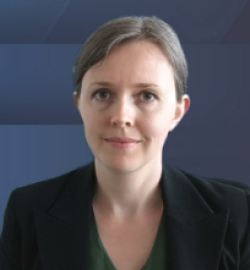
Brandl, Elisabeth

Brandl, Elisabeth
Business Development Manager
EVG

Brandl, Elisabeth

Abstract
Heavy data workloads have already driven the deployment of optical interconnects as a practical solution to the limitations of electronic data transfer. Especially with artificial intelligence (AI), the need for efficient data transfer is again immensely increased. Optical interconnects are now used in modern data centers and high-performance systems, enabling high-bandwidth, low-latency, and energy-efficient communication across chips and racks. Supported by advances in silicon photonics and system integration, these optical technologies have become a key enabler for scaling today’s large AI models and infrastructure.In this work, we present an overview of manufacturing approaches for silicon photonic components and their integration into various optical interconnect architectures. A particular emphasis is placed on advanced bonding techniques as an enabler for heterogeneous integration. We examine both die-to-wafer and wafer-to-wafer bonding strategies, highlighting their advantages: die-to-wafer bonding provides flexibility for selectively integrating high-performance components, while wafer-to-wafer bonding enables parallel, high-volume fabrication with improved uniformity and scalability. The discussed bonding technologies include temporary bonding, plasma-activated fusion bonding, oxide-free direct bonding, and hybrid bonding. Such methods enable the integration of diverse material systems, including III–V semiconductors for realizing efficient on-chip light sources, as well as thin-film lithium niobate for high-performance electro-optic modulation. By combining these materials with silicon photonics platforms, it becomes possible to leverage their complementary properties. III–V compounds offer high optical gain compared to Si, and lithium niobate has a high electro-optical efficiency. By integrating different material systems, the functionality and performance of integrated photonic circuits is significantly enhanced.By combining these advanced bonding techniques with scalable process flows, a versatile manufacturing toolbox is established, capable of supporting highly integrated, high-performance optical interconnect systems tailored to the stringent requirements of AI computing.

Biography
Elisabeth Brandl is business development manager at EV Group for temporary bonding and metrology. She holds a Master degree (DI) in technical physics from the Johannes Kepler University Linz specialized on nanoscience and - technology.Since 12 years she works at EVG and was, amongst other topics responsible for the UV laser debonding launch. She published several articles and papers in the field of temporary bonding and metrology.

Advanced Packing Conference
F To top
Flexiramics B.V Flexiramics B.V Wynn, Andy
Beyond Glass: Flexiramics for Next-Generation RF and Thermal Substrates

Wynn, Andy
CEO
Flexiramics B.V

Wynn, Andy

Abstract
Recent evaluations and early application trials have demonstrated that Flexiramics®, a European‑developed ceramic microfiber nonwoven reinforcement, can deliver measurable benefits in XY thermal spreading and RF/mmWave stability when integrated into advanced substrate and packaging materials. These results represent a new development in reinforcement architectures for high‑frequency and high‑thermal‑load electronics, offering an alternative to traditional woven glass fabrics.As devices move into the 28–110 GHz domain and thermal densities continue to rise, the limitations of glass‑reinforced dielectrics are becoming more pronounced. Woven glass introduces anisotropy, resin‑rich pockets, and local dielectric variation, all of which can affect signal uniformity and thermal performance. These constraints are increasingly visible in multilayer substrates, advanced packaging, and next‑generation RF systems.Flexiramics addresses these challenges through a continuous ceramic micro‑network that can be incorporated into existing polymer matrices and lamination processes.Recent test data and early customer evaluations indicate three key areas of impact:• XY thermal dissipation - application trials show that the ceramic network supports more efficient lateral heat spreading, helping reduce hotspot formation. This is designed to support improved thermal stability in high‑density architectures• RF/mmWave stability - initial RF measurements demonstrate stable dielectric behaviour across 30–110 GHz, with reduced sensitivity to local reinforcement effects. This is particularly relevant for communication, radar, sensing, and advanced packaging applications• Beyond glass - by eliminating woven‑fabric artifacts, Flexiramics provides a more uniform reinforcement environment. Early evaluations indicate more predictable electrical behaviour across the panel compared to glass‑based systemsBeyond technical performance, Flexiramics contributes to broader European strategic objectives. The platform is developed and manufactured within the EU, supporting regional supply‑chain resilience for advanced materials. Its scalable production approach enables both early‑stage prototyping and industrial‑scale deployment.The presentation will share new evaluation data, application examples, and insights from ongoing collaborations, illustrating how a new reinforcement architecture can help Europe advance toward more capable, efficient, and reliable electronic systems.

Biography
Andy is a technology leader with 30 years’ experience transformingnew technologies into successful global businesses. FormerCTO of Morgan Advanced Materials plc, $Billion FTSE 250multinational. Brings deep expertise in aligning innovationand business strategy across industries and geographies,including 6+ years based in China.​Led commercialization of $2B of new tech sales inrenewable energy, EVs, medical devices, semicon & more​Held senior exec roles (CTO, CEO, Board Director,Programme Director) with responsibility for global P&L,innovation, strategy, and major restructuringprogrammes​Built and scaled businesses internationally: launchedventures across Asia, built factories in China/ME/Asia,turned around US operations, and re-engineeredproduction lines worldwide​Entrepreneurship: Co-Founder of TTIP Talent, TTIPStrategy, PurEmissions, and BLOK Capital​Educator & thought leader: keynote speaker, MBA facultyat IE & Warwick Business Schools, and author ofTransforming Technology into Profit, Cracking theInnovation Code, and Building an Innovation Powerhouse.​

Start Up Pitches
Fraunhofer IPMS-CNT Guhl, Conrad
Functional Silicon Interposers for 2.5D integration

Guhl, Conrad

Fraunhofer IPMS-CNT

Abstract
The ever-rising demand for computational power increase poses a great challenge, one solution is to combine multiple functions as chiplets with high I/O density employing a silicon interposer. The key to successful combination of chiplets in a system is high I/O density, thus small pitches approaching BEoL dimensions. Usage of silicon interposers with damascene based interconnect lines has the key benefit of a mature technology easily scalable to sub µm dimensions. Unfortunately, Silicon interposers with damascene based RDLs are comparably expensive. One industry reaction to the cost issue was miniaturization of Silicon interposers for cost savings, namely EMIB. Another possible consequence of the cost issue for Silicon interposers is to raise their value by integrating passive devices to realize a functional interposer.In the contribution we present the concept of integrated capacitors and resistor networks. By utilization of Silicon based production steps it is possible to integrate 3D capacitors in silicon interposers realizing capacity densities of up to 400nF/mm². As the capacitors move from a location next to active devices to directly below the active devices the wiring length can be reduces from several mm to few µm. The unique combination of close proximity high density capacity is crucial and allows to work e.g. without capacitor ladders.Advanced chiplet interconnection schemes like UCIe 3.0 and mobile hardware trends to lower switching voltages further increase the demand for integrated passive devices. To realize high data transfer rates like 64 GT/s in UCIe 3.0 impedance matched transmission lines are crucial. One way to realize these is integration of distinct passive devices. For ultra low power devices not only the operation voltage, but also the voltage tolerance is minimal. Such low tolerances are challenging to realize and demand a maximum capacity in ultimate proximity to the active devices. Both challenges can be tackled by functional silicon interposers.

Biography
Conrad Guhl:2009-2015 Bachelor & Master on Materials Science at Friedrich-Schiller-Universität Jena; Focus on metallic materials2015-2018 PhD in Materials Science at Technische Universität Darmstadt; XPS on battery cathode materials2019-2023 Scientist for Chemical Mechanical Polishing at Fraunhofer IPMS; Focus on design process interactions2024-open Group Leader Interconnect Technologies; work package leader in EU Chips act project “Advanced Packaging and Heterogeneous Integration for Electronic Components and Systems”

Advanced Packing Conference
Fraunhofer IZM-ASSID Bickel, Steffen
Pilot-line implementation of advanced die-to-wafer integration based on hybrid and fusion bonding processes

Bickel, Steffen

Fraunhofer IZM-ASSID

Abstract
Advanced electronic packaging technologies enable next-generation system performance, driven by the increasing demands of AI, high-performance computing (HPC) and heterogeneous system integration. In this context, the APECS pilot line plays a central role in Europe by bridging the gap between research and industrial manufacturing, enabling the transfer of advanced packaging technologies into scalable and production-ready solutions. Fraunhofer IZM-ASSID contributes to this effort by developing and validating core process modules for chiplet integration. Focusing, on die-to-wafer (D2W) bonding technologies, this work presents a technology-driven evaluation of low-temperature fusion bonding using both TEOS and SiCN as well as hybrid bonding at an interconnect pitch of 10 µm. Die sizes range from 4 mm x 4 mm to 9 mm x 9 mm and their corresponding thickness from 775 µm down to 100 µm. Adressing critical processing challenges such as surface preparation, die handling and bonding yield with respect to high component throughput as well as introducing novel characterization techniques, the study is conducted by Fraunhofer IZM-ASSID in close collaboration with Fraunhofer IMWS. At first, the results point out the importance of precise process control on 300 mm wafer, paritcularly for dielectric deposition, chemical-mechanical polishing and the cleaning of singulated wafers. From a pilot-line perspective, the bonding yield for a given process is the most important metric. Therefore, densely populated 300 mm wafers were characterized by non-destructive methods. Only bonding areas exhibiting no detectable voids were considered for yield analysis. While bonding yields beyond 95% are obtainable using 4 mm dies for a given process-of-record (POR) flow, they drop distinctly in case of larger dies, thus requiring extensive adjustments and optimization, respectively. The presented work provides a significant contribution to the development and qualification of high-throughput fine-pitch D2W bonding processes as a key enabling technology for chiplet integration within the APECS pilot line framework.

Biography
Steffen Bickel received a diploma degree in materials science in 2011 and a PhD degree in electrical engineering in 2025, both from TU Dresden. In 2021, he joined Fraunhofer IZM-ASSID and currently manages research projects to further develop wafer level packaging technologies for quantum computing applications and bonding technologies for heterogeneous chiplet integration.

Advanced Packing Conference
G To top
GlobalFoundries GlobalFoundries Kneitz, Stefan
Coming Soon

Kneitz, Stefan

GlobalFoundries

Kneitz, Stefan

Abstract
Coming Soon

Biography
Coming Soon

Future Disruptions
H To top
Hitachi Energy Ltd Hitachi Energy Ltd Keller, Tobias
The evolvement of the largest and most complex structure built by humans and its influence on Power Semiconductors

Keller, Tobias
Vice President, Head of global Product Management, Portfolio & Marketing
Hitachi Energy Ltd

Keller, Tobias

Abstract
The electrical power grid has been built up over decades and many previously isolated sub-grids are connected to each other. The integration of renewable energy sources now leads to a sharp increase in power semiconductors in the distribution network with technologically very interesting prospects.

Biography
Tobias Keller graduated in 2004, from University of applied science Aargau, the Electrical Engineering Faculty, with a degree in power electronics, thermodynamics and electrical machines. At the end of 2004, he joined ABB Excitation systems and Synchronizing equipment business (Turgi, Switzerland) and held various engineering position until 2008. He holds the first patent on MEGATROL, ABB’s smart power package solution for reliable starts of gas turbines or any synchronous machine and another patent quenching arc faults in excitation systems. In 2008 he became the Head of global Technology and Support for ABB’s Excitation systems and Synchronizing equipment business. Between 2009 and 2015 he was the Vice President global Products and Marketing ABB Excitation systems and Synchronizing equipment and High Power Rectifier business. Starting from 2016 until 2019 he held the Vice President position for Vehicle Integration Engineering business in ABB railway traction. Since April 2019, he is the Vice President of global Product Management in ABB Semiconductors (Lenzburg, Switzerland) now HITACHI ENERGY Semiconductors and a strong supporter of SiC used in power electronics based on his application know how from traction and industrial applications. Tobias is responsible for the global Product Management and Marketing of any Power Semiconductor from Hitachi Energy as well as responsible for BIMOS power semiconductors R&D (Chips and packages, Si and SiC). Tobias Keller is a senior member of IEEE (20127) and co-author of various papers.

Electrification and Power Semiconductors
I To top
imec imec Vanhoutte, Tom
Moderator

Vanhoutte, Tom
Partner - imec.xpand
imec

Vanhoutte, Tom

Abstract
Coming Soon

Biography
Tom Vanhoutte is founding partner of imec.xpand, an independently managed early stage and growth fund that invests in start-ups where knowledge, expertise, network and/or infrastructure of imec, the world-renowned semiconductor R&D center, plays a differentiating role in the success of the company. The two imec.xpand funds raised over 400 million EUR and are amongst the best performing venture capital funds globally.

imec ITF - Building the silicon backbone of Europe’s AI leadership
imec Miller, Andy
Panelist

Miller, Andy
Department Director, 3D and Silicon Photonics Technology
imec

Abstract
Panelist

Biography
Coming soon.

Entegris
imec imec Marent, Katrien
Closing Remarks

Marent, Katrien
EVP & Chief Marketing and Communications Officer
imec

Marent, Katrien

Abstract
Coming Soon

Biography
Katrien Marent has an engineering degree in microelectronics. She joined imec in 1992 as analog design engineer and specialized in design of low-noise readout electronics for high-energy physics. In 1999, she became press responsible and scientific editor at imec's business development division and was responsible for authoring and editing the research organization's numerous company technical documents and publications. In 2001, she was appointed corporate communications director at imec. Her responsibilities expanded in August 2007, when she got the position of external communications director including corporate, marketing and outreach communications. In October 2016, she became VP corporate, marketing and outreach communication. Since April 2020 she is Executive Vice President & Chief Marketing and Communications Officer and member of the executive board of imec.

imec ITF - Building the silicon backbone of Europe’s AI leadership
imec imec Vandenameele, Patrick
Orchestrating a scalable AI revolution

Vandenameele, Patrick
CEO
imec

Vandenameele, Patrick

Abstract
Artificial intelligence is becoming the defining technology of our era, but its long-term impact depends on one critical challenge: scalability. As AI evolves toward complex, agentic systems operating from cloud to edge, demands on compute, memory, and connectivity are growing at an unprecedented pace. This keynote explores how sustaining the AI revolution requires innovation across the entire technology stack, from advanced CMOS and heterogeneous integration to photonic interconnects and system-level co-optimization. Looking further ahead, emerging paradigms such as quantum and brain-inspired computing may unlock new forms of efficient intelligence. Ultimately, scalable AI will not emerge from a single breakthrough, but from orchestrating a global ecosystem of technologies, disciplines, and innovators.

Biography
Patrick Vandenameele is Chief Executive Officer at imec - a globally recognized R&D center specializing in nanoelectronics and digital technologies - since April 1, 2026. His leadership underpins imec’s commitment to addressing market-driven application challenges while advancing its world-class technology platforms through targeted internal investments and external collaborations.Prior to this appointment as CEO, he served as Executive Vice President and Co-Chief Operating Officer at imec, where he was overseeing and shaping the organization's R&D strategy and its execution. In this position, Patrick was responsible for shaping and driving the center’s innovation agenda, ensuring the alignment of research initiatives with emerging market needs, partner priorities and technological frontiers. Previously, as chief portfolio officer at imec until early 2024, he spearheaded strategic initiatives spanning business development, portfolio management, and venture creation. Holding a PhD from KU Leuven, Patrick began his journey with imec in 1996, contributing to the wireless communications program. In 2000, he transitioned to entrepreneurship, founding and leading several deep-tech ventures, three of which were built on imec technology. Patrick also held senior positions at top semiconductor firms like Qorvo and Hisilicon/Huawei, leading 11 product launches and overseeing over 100 million units shipped. After returning to imec in 2017, Patrick has been instrumental in expanding imec’s venture development activities, working closely with the deep-tech venturing fund imec.xpand to strengthen imec’s position as a pioneer in technology-driven solutions.

imec ITF - Building the silicon backbone of Europe’s AI leadership
imec imec Latré, Steven
What does an AI Workload actually need from silicon? imec's cross stack view

Latré, Steven
VP AI
imec

Latré, Steven

Abstract
As AI workloads increasingly dictate hardware requirements, the semiconductor industry needs a common, vendor-neutral language to connect process and packaging decisions to real-world AI performance. This talk introduces imec's AI Stack: a benchmarking platform and layered framework that maps AI workloads — from inference to training — down through system architecture, device integration, and ultimately to process and materials choices such as lithography parameters and node scaling. Drawing on early results, including a GPU total-cost-of-ownership analysis, we show how fab-level decisions ripple through to workload economics, and outline imec's ambition to build an open ecosystem where hardware and AI software communities can jointly optimise the stack.

Biography
Steven Latré is Vice President AI at imec, the worldwide leading research centre on semiconductors. In this role, he’s responsible for imec’s AI portfolio, focusing mainly on the intersection of hardware and software and how next generation AI workloads drive the semiconductor roadmap. Steven has a 20+ year career in AI, leading and scaling highly technical teams on the intersection of AI and hardware. Previously he was a professor in AI at the University of Antwerp, Chief AI Officer at OpenChip, a full stack chip player in HPC and AI, and was already previously Vice President AI at imec.

imec ITF - Building the silicon backbone of Europe’s AI leadership
imec imec Holsteyns, Frank
From Vision to Impact: Three Years of NanoIC Enabling Future Semiconductor Technologies

Holsteyns, Frank
VP R&D Unit Process & Modules
imec

Holsteyns, Frank

Abstract
Three years after its launch, NanoIC grows into a collaborative European innovation ecosystem that accelerates the development of the chips of the future. Driven by a shared ambition to strengthen the semiconductor innovation and expand manufacturing capabilities, NanoIC brings together industrial and research partners around advanced technology platforms and infrastructure. By highlighting key achievements in Logic, Memory and Heterogeneous Integration, we showcase how collaborative R&D and shared infrastructure can accelerate innovation and reduce barriers to technology development. Engagement with companies, leveraging this new ecosystem, allows to jointly shape the next generation of semiconductor technologies together.

Biography
Frank Holsteyns has been serving as the VP of R&D at imec, leading the Unit Process and Module Department since July 1, 2023. Before stepping into this role, he was the director of the same department, where he managed various process-development-focused groups, including surface and interface processing, etch, thin film deposition, epitaxy, plating, chemical mechanical polishing, layer transfer, and assembly.Frank's journey at imec began in 2000, where he concentrated on wet cleaning research for semiconductor devices. His work in this area culminated in a PhD in Bio Engineering (surface chemistry) from KU Leuven, Belgium. In 2006, he transitioned to Lam Research AG in Villach, Austria, as a research scientist. There, he coordinated a university and research network focused on fluid dynamics, particularly cavitation, droplet impact, wetting, and dewetting.In 2012, Frank returned to imec, taking on the role of manager for the Surface and Interface Processing Group. In this position, he specialized in wet clean and etch processes, as well as isotropic dry etches.

imec ITF - Building the silicon backbone of Europe’s AI leadership
imec imec Hoofman, Romano
Design enablement services: lowering the barrier for IC design companies

Hoofman, Romano
Strategic Development Director
imec

Hoofman, Romano

Abstract
As part of the EU Chips Act, the EU Chips Design Platform (EuroCDP) has been launched. EuroCDP's mission is to lower the barrier for fabless IC design companies, in particular startups. This will be done by lowering the technical barriers and the cost of the design process, plus in addition dedicated venture development together with private investors. EuroCDP is designed as a one-stop marketplace for startups, SMEs, and research teams, offering streamlined access to advanced design tools, manufacturing, IP, training, and funding.

Biography
Romano Hoofman is Strategic Development Director at imec since 2016. He is responsible for the coordination of both the EU Chips Design Platform and the EUROPRACTICE Service. In addition, his team is responsible for providing technology access and design enablement for the NanoIC pilot line, 2D-PL and SPINS (Quantum pilot line). He started his career in industry, where he worked as a Principal Scientist at Philips Research and later on NXP Semiconductors. He covered many different R&D topics, ranging from CMOS integration, advanced packaging, thin film batteries, photovoltaics and (bio)sensors. Romano received his PhD from the Technical University of Delft in 2000, where he investigated charge transport in semi-conducting polymers. He has authored more than 30 publications and holds more than 10 patents in various research areas.

imec ITF - Building the silicon backbone of Europe’s AI leadership
imec imec Sommer, Grit
Beyond Automotive: chiplets as the Foundation for Autonomous Edge Platforms

Sommer, Grit
Regional Managing Director
imec

Sommer, Grit

Abstract
Edge High Performance Compute is becoming the “brain” of autonomous systems, enabling the rapid growth of L2+ and future autonomous mobility capabilities. However, the automotive industry faces a fundamental dilemma: compute requirements are increasing exponentially, driven by AI and advanced perception workloads, while the global automotive market remains relatively flat and cannot absorb the rising costs associated with leading-edge semiconductor technologies.Imec believes interoperable chiplet architectures provide the path forward. By decomposing complex system-on-chip designs into modular building blocks, chiplets enable heterogeneous integration of compute, AI, safety, and memory functions, each optimized on the most appropriate technology node. This approach improves scalability, yield, cost efficiency, supply-chain resilience, and platform reuse while supporting the transition toward software-defined vehicles.To accelerate adoption, imec is bringing together complementary initiatives across the chiplet value chain. The Automotive Chiplet Forum (ACF) aligns industry stakeholders around open, interoperable chiplet standards, while the Automotive Chiplet Program (ACP) advances pre-competitive research and technology development. Complementing these efforts, the new Chiplet Acceleration Center (CAC) at imec Germany supports design enablement, prototyping, and the path toward industrial deployment. Together, they help de-risk development, advance quality and reliability, and accelerate the transition from chiplet innovation to real-world automotive applications.Building on the success of ACP, imec is expanding its vision beyond automotive with the launch of the Autonomous Edge Chiplet Program (AECP), addressing shared compute needs across robotics, humanoids, aerospace, and security applications. Complemented by the development of a reference autonomous edge platform, this cross-industry strategy aims to accelerate innovation, reduce costs, strengthen resilience, and establish interoperable chiplets as the foundation for next-generation autonomous systems.

Biography
Dr. Grit Sommer is the Regional Managing Director of imec Germany, a position she has held since July 2026. With almost three decades of experience in the semiconductor industry, she is recognized as a strategic technology leader, transformative executive, and accomplished people manager, combining deep technical expertise with a strong track record of building high-performing global organizations. Prior to joining imec, Dr. Sommer spent 20 years with Infineon Technologies, where she held a series of international leadership positions across Germany and Singapore. Most recently, she served as Senior Director Global Product Engineering Digitalization, leading the digital transformation of end-to-end product engineering across a global network of manufacturing and R&D sites. In this role, she drove the adoption of advanced analytics and artificial intelligence, enabling significant improvements in product development efficiency, yield optimization, and quality management. Throughout her career, Dr. Sommer has successfully led multicultural teams across Europe, Asia, and the Americas, managing organizations with of up to 50 experts and influencing more than 1,000 employees worldwide. Her expertise spans semiconductor technology, advanced packaging, product engineering, manufacturing excellence, digitalization, and innovation management. She has consistently delivered business impact through strategic program leadership, operational excellence initiatives, and technology-enabled transformation. Before her tenure at Infineon, Dr. Sommer held research and leadership roles at the Fraunhofer Institute for Reliability and Microintegration (IZM), where she established and led advanced RF modelling and simulation activities and managed numerous industry and publicly funded research programs. Dr. Sommer holds a PhD (Dr.-Ing.) in Electrical Engineering and Computer Science from TU Berlin, specializing in RF modelling and design optimization. She also earned her Engineering Degree (Diplom-Ingenieur) in Electrical Engineering from TU Berlin with distinction. In addition to her executive responsibilities, she has served as a board member supporting the strategic development of Fraunhofer IZM and has contributed to industry governance and leadership selection processes. Driven by curiosity, innovation, and an entrepreneurial mindset, Dr. Sommer is passionate about advancing semiconductor technologies and strengthening Germany's role in the global microelectronics ecosystem.

imec ITF - Building the silicon backbone of Europe’s AI leadership
imec imec Shamuilia, Sheron
Chips Act 2.0 and SSTS: Building Europe's Next Semiconductor Advantage

Shamuilia, Sheron
ESG Program Director
imec

Shamuilia, Sheron

Abstract
As Europe moves from capability creation to competitiveness, the success of Chips Act 2.0 will depend not only on research infrastructure, pilot lines and manufacturing capacity, but also on the intelligence, innovation and ecosystem collaboration required to sustain them. This presentation explores how imec's Sustainable Semiconductor Technologies & Systems (SSTS) program combines its Assess and Improve activities to create competitiveness intelligence across the semiconductor value chain. By connecting manufacturers, suppliers, researchers, system companies and emerging design ecosystems, SSTS helps address challenges related to sustainability, resilience, resource security and future design enablement. The presentation discusses how such ecosystem intelligence can contribute to Europe's long-term competitiveness and support the ambitions of Chips Act 2.0.

Biography
Sheron Shamuilia leads imec's ESG strategy, embedding sustainability across semiconductor R&D, operations, governance, and strategic partnerships. Her work focuses on positioning sustainability as a driver of responsible innovation, ecosystem resilience, circularity, and long-term value creation. With over 15 years of experience spanning the European Commission, corporate public affairs, and the semiconductor industry, including Cadence, she has worked at the intersection of technology, policy, innovation, and business strategy. Holding a Ph.D. in semiconductor physics, Sheron brings a unique combination of technology expertise, policy insight, and sustainability leadership, helping bridge research, industry, and government to accelerate sustainable innovation and competitiveness across the semiconductor ecosystem.

imec ITF - Building the silicon backbone of Europe’s AI leadership
imec imec Van den Bosch, Anne
Panelist

Van den Bosch, Anne
VP Strategic Public Policy & Invest for R&D Ecosystems
imec

Van den Bosch, Anne

Abstract
Coming Soon

Biography
Coming Soon

imec ITF - Building the silicon backbone of Europe’s AI leadership
imec imec Van den hove, Luc
Orchestrating a scalable AI revolution

Van den hove, Luc
Chairman
imec

Van den hove, Luc

Abstract
Artificial intelligence is becoming the defining technology of our era, but its long-term impact depends on one critical challenge: scalability. As AI evolves toward complex, agentic systems operating from cloud to edge, demands on compute, memory, and connectivity are growing at an unprecedented pace. This keynote explores how sustaining the AI revolution requires innovation across the entire technology stack, from advanced CMOS and heterogeneous integration to photonic interconnects and system-level co-optimization. Looking further ahead, emerging paradigms such as quantum and brain-inspired computing may unlock new forms of efficient intelligence. Ultimately, scalable AI will not emerge from a single breakthrough, but from orchestrating a global ecosystem of technologies, disciplines, and innovators

Biography
Luc Van den hove is President and CEO of imec since July 1, 2009. Before he was executive vice president and chief operating officer. He joined imec in 1984, starting his research career in the field of silicide and interconnect technologies. In 1988, he became manager of imec’s micro-patterning group (lithography, dry etching); in 1996, department director of unit process step R&D; and in 1998, vice president of the silicon process and device technology division. In January 2007, he was appointed as imec's EVP & COO. Luc Van den hove received his PhD in electrical engineering from the KU Leuven, Belgium.In 2023, he was honored with the Robert N. Noyce medal for his leadership in creating a worldwide research ecosystem in nanoelectronics technology with applications ranging from high-performance computing to health.In 2025, he received an honorary distinction from the Flemish Community in recognition of his impressive role in strengthening Flanders as a leading innovative region. He has authored or co-authored more than 200 publications and conference contributions.Starting in April 2026, he took on a new role as Chair of imec’s Board of Directors.

CxO Summit
INFICON Inc. INFICON Inc. Behnke, John
Coming Soon

Behnke, John
General Manager Smart Manufacturing
INFICON Inc.

Behnke, John

Abstract
will be announced later

Biography
Mr. Behnke has over 40 years of semiconductor industry experience. As the GM of INFICON’s FPS Product Line and Head of its IMS Marketing team, John leads a global team that develops and deploys Smart Manufacturing software and hardware solutions which improve factories performance. INFICON’s comprehensive Digital Twin of a factory enables advanced Factory Scheduling, optimized WIP movement and other advanced capabilities.He is also a Co-Chair of the Semi North America Smart Manufacturing Chapter as well as a founding member of Semi’s Smart Global Executive Committee. Prior to his current role at FPS John served as: the President of Novati Technologies, SVP and GM of the Semiconductor Group at Intermoleculor, CVP for Front End Manufacturing and Tech Transfers at Spansion and Director of Operations at AMD's Austin Fab 25

Fab Management Forum
Infineon Infineon Recklies, Joerg
Coming Soon

Recklies, Joerg
Executive Vice President Frontend
Infineon

Recklies, Joerg

Abstract
Coming Soon

Biography
Coming Soon

Fab Management Forum
Infineon Technologies Infineon Technologies Grassmann, Andreas
Session Chair

Grassmann, Andreas
Vice President
Infineon Technologies

Grassmann, Andreas

Abstract
Coming Soon

Biography
Coming Soon

Advanced Packing Conference
Infineon Technologies Infineon Technologies Kessler, Angela
We power AI from grid to core

Kessler, Angela
Senior Principal Engineer Package Concepts
Infineon Technologies

Kessler, Angela

Abstract
We are all part of a technological revolution driven by AI, which is gaining momentum unpredictably. AI not only has the potential to significantly change our daily lives through digital assistants, financial services or programming new ways, but it also transforms and reshapes every part of the computing market. The heart of this transformation is the enormous power requirement of AI technologies.To meet accelerating AI compute demand, next generation processors will need 2–4 kW per GPU, pushing rack power toward 1 MW+ by 2030. Increasing GPU cluster densities demands new power architecture designs that boost efficiency, thermal performance, and power delivery density while ensuring high reliability.Today’s AI racks use 1‑phase PSUs to create a 50 V bus that is distributed to the compute trays and will support up to 250kW rack power. IBCs and high‑density DC‑DC stages supply <1 V GPU core power, making optimized conversion essential as currents rise into the thousands of amps.Electricity and cooling are the major lever affecting GPU infrastructure TCO, often more impactful than minor differences in hardware acquisition costs. Even a seemingly small efficiency drop in a large GPU cluster translates to substantial financial impact. A reduction in cooling costs can be achieved not only through high efficiency but also through effective cooling due to a low Rth of the components.This talk presents the path from grid to core for powering AI with focus on DC-DC power modules and their thermal management.

Biography
Angela Kessler has been with Infineon Technologies AG since 2000. After completing her diploma in Chemistry in Göttingen, she received her PhD in Physical Chemistry at the University of Regensburg. She has worked in package development for Power and Sensor Systems, Automotive, and Green Industrial Power divisions. Her current focus is on concepts for energy-efficient packages with high power densities, for power delivery from the grid to the processor core for AI and data centers.

Advanced Packing Conference
Infineon Technologies Dresden AG & Co. KG Jentzsch, Julia
Challenges of Digital Transformation in an Established Semiconductor Factory

Jentzsch, Julia

Infineon Technologies Dresden AG & Co. KG

Abstract
Through a digital transformation project at Infineon’s Dresden site, our goal is to implement a coordinated, holistic digitalization strategy for the site. This involves fundamentally rethinking the organization, processes, and collaboration. The focus is not only on the technical implementation of individual projects, but rather on supporting employees through the transformation phase by further developing their work methods and adapting and introducing new business processes.

Biography
Julia Jentzsch has been with Infineon Dresden since 2011. After holding positions in industrial engineering, implementing automation projects, and maintenance manager, she has led the Digital Transformation Dresden department since 2025. Her focus is on the successful implementation of digital transformation project at Infineon Dresden.

Fab Management Forum
Infineon Technologies Dresden AG & Co.KG Thyssen, Norbert
Powering AI - Infineon's Smart PowerFab

Thyssen, Norbert
Senior Director R&D Technology
Infineon Technologies Dresden AG & Co.KG

Abstract
The Power Management application field is driven by several market changes. Ai-Server do develop new power bus configurations and independant electrical machines, e.g. cars and humanoids need smart power configurations. Giving some insight on these developments and the consequences on technology needs will be connected to the newest Smart Power Fab in Dresden of Infineon, shwing how this will contrinute. The talk tries to show how dynamic and fast market changes search for a supply chain set-up that is able to deliver solutions.

Biography
- PhD in Physics (Diplom: RWTH Aachen / PhD: Research Center Jülich and University of Erlangen)- 28 years of experience in semiconductor technologies with focus in Research & Development & Innovation in a manufacturing environment on 200mm and 300mm- experienced in custoer partnership and joined projects with many partners in the European context- Technology Knwoledge: DRAM. embedded Flash, BCD, MEMS, Optics, Sensors, Power, Smart Power, embedded Poser)

Electrification and Power Semiconductors
Infinitesima Infinitesima Haspel, Dan
High-Speed AFM Metrology for Advanced Packaging: Enabling High-Yield Hybrid Bonding at Sub-Micron Pitch

Haspel, Dan

Infinitesima

Haspel, Dan

Abstract
Advanced packaging has become a primary driver of semiconductor performance, with hybrid wafer bonding emerging as the key enabler of 3D integration. As bonding pitches scale toward sub-1-micron dimensions, the process window tightens: copper pad recess, dielectric roughness, and wafer-scale flatness must all be controlled simultaneously to achieve void-free, high-yield bonding interfaces. This creates a metrology “blind spot” – the need to capture sub-nanometre roughness and millimetre-scale topography across an entire wafer without sacrificing high-volume manufacturing (HVM) throughput. Atomic Force Microscopy (AFM) has long been the gold standard for 3D surface resolution, but its historic speed constraints have confined it to R&D. This paper presents a paradigm shift in in-line process control using the Metron®3D, a hybrid optical-AFM system. Combined with a high-speed wafer stage and surface detection, it enables dense sampling across full 300 mm wafers at speeds compatible with mass production – measuring copper pad recess with picometre repeatability at throughputs exceeding 60 wafers per hour under standard sampling plans. We demonstrate that a single high-speed AFM platform can deliver comprehensive, multi-scale characterisation – from local copper dishing and dielectric roughness to macro-scale wafer topography – at sub-nanometre precision. This makes it ideally suited to pre-bonding characterisation of post-CMP wafers, ensuring interfaces meet the stringent requirements for high yield hybrid bonding. Results from a 3D integration development partner will be presented, proving that the multi-scale data density of high-speed AFM is essential to securing bonding interfaces in advanced semiconductor manufacturing. By moving AFM out of the R&D lab and onto the production line, this approach closes the metrology gap that today constrains hybrid-bonding yield – accelerating the cost-effective scaling of 3D-integrated devices for the AI and high-performance-computing era.

Biography
Dan Haspel is Product Manager at Infinitesima Limited, the UK company behind Rapid Probe Microscopy (RPM) — a breakthrough nanoscale metrology technology enabling true 3D imaging for next-generation semiconductor manufacturing.With a PhD in Materials Science from Loughborough University and a background spanning Oxford Instruments and academic research, Dan brings together deep technical knowledge and commercial expertise to drive Infinitesima's product strategy. He works closely with semiconductor manufacturers, research institutions, and industry partners to translate cutting-edge science into real-world solutions.Dan is passionate about bridging the gap between complex technology and the people who use it — from advanced metrology to the practical adoption of modern digital tools within high-tech organisations.

Advanced Packing Conference
INGAGE INGAGE Robert, Philippe
NEMS-Based Inertial Sensors: Enabling Navigation-Grade Performance for High-Volume Autonomous Applications

Robert, Philippe
CEO
INGAGE

Robert, Philippe

Abstract
Reliable navigation remains a critical challenge for autonomous systems operating in environments where GNSS signals are unavailable or degraded. From autonomous vehicles and drones to industrial robots, accurate positioning requires inertial sensors capable of maintaining navigation performance during extended GNSS outages.While MEMS inertial sensors have become ubiquitous thanks to their compact size, low power consumption and low manufacturing cost, their performance remains insufficient for many navigation-grade applications. Conversely, existing high-end inertial solutions deliver the required accuracy but are often too bulky and expensive for deployment in high-volume markets.This presentation introduces a new generation of MEMS inertial sensors based on ultra-sensitive nano-strain-gauge transduction technology. Developed over more than 15 years of research at CEA-Leti and protected by an extensive patent portfolio, this breakthrough sensing approach significantly enhances the detection of mechanical motion and enables performance levels beyond the limits of conventional capacitive MEMS technologies.The talk will present the fundamental principles of nano-strain-gauge sensing, its integration into MEMS accelerometers and gyroscopes, and the expected benefits in terms of bias stability, noise performance, scale-factor stability and overall inertial navigation accuracy. Particular attention will be given to the challenges associated with transferring advanced laboratory technology into a manufacturable industrial solution compatible with high-volume semiconductor processes.The presentation will also provide an overview of the technology industrialization roadmap pursued by iNGage, a fabless Deeptech company founded in 2025 to bring this innovation to market. By combining navigation-grade performance with MEMS scalability, nano-strain-gauge inertial sensors have the potential to unlock a new generation of cost-effective navigation systems for autonomous mobility, robotics and other demanding positioning applications.

Biography
Philippe Robert is CEO and co-founder of iNGage, a deeptech startup developing a new generation of high-performance MEMS sensors. He holds a PhD in Microtechnologies and began his career at the startup SILMAG, developing advanced magnetic sensor technologies for data storage, before joining THALES to work on high-end MEMS inertial sensors for aerospace and defense applications.He joined CEA-Leti in 2001, where he held successive leadership roles, including Head of the MEMS Sensors Laboratory and Head of the Microsystems Department (120+ people), before leading Business Development for Microsystems.In 2025, he founded iNGage as CEO & CTO, leading corporate strategy, fundraising, and execution.He has authored over 50 scientific publications and holds more than 60 patents, including more than 20 related to the M&NEMS architecture at the core of iNGage’s innovation.Philippe also contributes to the international MEMS community through expert evaluations (HCERES, EIC) and leadership roles in major conferences such as IEEE MEMS, IEEE Transducers, and Eurosensors.

MEMS & Imaging Sensors Summit
Injectpower Andreucci, Philippe
Ultra miniaturized rechargeable solid-state micro battery technology for new generation of implantable medical devices

Andreucci, Philippe
Chief Executive Officer
Injectpower

Abstract
Powering the Future of Digital Health: Ultra-Miniaturized All-Solid-State Microbatteries for Next-Generation Implantable Medical DevicesThe rise of digital health and personalized medicine has fueled an unprecedented demand for autonomous, smart implantable medical devices (IMDs). Monitoring and treating chronic pathologies—such as glaucoma in ophthalmology, intracranial pressure in neurosurgery, or arrhythmia in cardiology—require continuous, highly reliable physiological data tracking. However, traditional battery technologies represent a critical bottleneck, as their size, rigid form factors, and chemical leakage risks severely limit the miniaturization and safety of long-term implants.This paper introduces INJECTPOWER’s breakthrough energy solutions based on wireless rechargeable, all-solid-state microbatteries tailored specifically for high-density, ultra-miniaturized IMDs. Leveraging over 20 years of foundational R&D at CEA-Leti and protected by a robust portfolio of more than 40 patents, these microbatteries achieve dimensions as thin as a human hair while delivering unrivaled volumetric energy density and hermetic safety.By eliminating liquid electrolytes, this all-solid-state chemistry eliminates the risk of toxic leakage, ensuring high biocompatibility and excellent thermal stability during wireless charging cycles (such as RF or inductive powering). This technology enables a new paradigm of completely autonomous, micro-scaled implants capable of providing continuous, representative medical data over years of implantation.We will present the electrochemical performance, cycling stability, and integration architecture of these microbatteries. Finally, we will discuss the scaling-up strategy and industrial roadmap within the framework of the European IPCEI Health (Tech4Cure) program, leading toward a first certified commercial product on the market by 2029.

Biography
Philippe AndreucciCo-founder & CEO of INJECTPOWER | Deep Tech Entrepreneur & Board MemberBiographyPhilippe Andreucci is a seasoned deep-tech entrepreneur and executive leader with over 25 years of experience driving breakthrough innovations from laboratory research to global markets. Throughout his career, he has successfully operated at the intersection of micro-technologies, nanosystems, and life sciences, combining strong technical expertise with a proven track record in fundraising, corporate governance, and international business development.Philippe began his leadership journey at CEA-Leti, a world-renowned microelectronics research institute, where he served as Head of Nanosystems Programs. During this tenure, he co-founded the Alliance for Nanosystems VLSI—a prestigious, multi-year international research collaboration between the CEA and the California Institute of Technology (Caltech), established alongside Professor Michael Roukes.Driven by an entrepreneurial vision, Philippe transitioned from institutional leadership to venture creation. He co-founded and led APIX Analytics, a company specializing in miniaturized gas chromatography systems for industrial and environmental applications. Under his leadership as CEO, APIX successfully industrialized its technology, raised significant venture capital and additional fundings, and established a strong international footprint.Following this success, Philippe co-founded INJECTPOWER in 2020, a pioneering deep-tech company disrupting the implantable medical device sector. The company manufactures ultra-miniaturized, wireless rechargeable all-solid-state microbatteries that provide autonomy to a new generation of monitoring and treatment solutions for chronic diseases (such as glaucoma, cardiovascular, and neurological disorders). Under his guidance, INJECTPOWER secured a strategic position within the prestigious European IPCEI Health (Tech4Cure) program, established key commercial partnerships in the US, and is currently on track for its first product certification by 2029.An active figure in the tech ecosystem, Philippe serves as a Board Member for several high-growth startups, where he provides strategic counsel on corporate scaling, venture financing, and intellectual property management.Core ExpertiseDeep Tech Entrepreneurship & Leadership: Proven ability to build, fund, and scale companies with highly complex, hardware-and-software integrated technologies.International Ecosystem Building: Established track record of forging high-level academic and industrial alliances between Europe and the United States (e.g., Caltech, US clinical partners).Venture Capital & Corporate Finance: Expert in structuring mixed financing strategies, combining multi-million dollar equity rounds (VC) with non-dilutive sovereign funding (IPCEI, state grants).Governance & Advisory: Experienced board member guiding early-stage and scaling startups through critical pivots, IP valorization, and growth phases.Vision Statement: "Miniaturized, reliable energy is the true gateway to tomorrow's digital health. By giving implantable devices the power to monitor chronic conditions autonomously, we are shifting medicine from reactive treatments to proactive, life-saving data intelligence."

MEMS & Imaging Sensors Summit
J To top
JCET Group JCET Group Antonicelli, Roberto
Session Chair

Antonicelli, Roberto
Senior Director, Strategy & Business Innovation
JCET Group

Antonicelli, Roberto

Abstract
Coming Soon

Biography
Coming Soon

Advanced Packing Conference
K To top
KAIST KAIST Jang, Young Jae
Autonomous Factory with Physical AI

Jang, Young Jae
Professor
KAIST

Jang, Young Jae

Abstract
Coming Soon

Biography
Young Jae Jang received his Ph.D. in Mechanical Engineering from the Massachusetts Institute of Technology (MIT) in 2007, and dual M.S. degrees in Mechanical Engineering and Operations Research from MIT in 2001. He earned his B.S. in Aerospace Engineering from Boston University in 1997. He is currently a Professor in the Department of Industrial and Systems Engineering at the Korea Advanced Institute of Science and Technology (KAIST) and the Founding Director of the Center for KAIST Manufacturing Physical AI, where he leads research on next-generation autonomous manufacturing systems. In parallel, he is the CEO and Co-founder of DAIM Research Corp., the leading startup commercializing AI-based manufacturing powered by Physical AI technology. DAIM’s platforms have been successfully deployed by major global manufacturers, including Samsung Electronics, LG Electronics, SK On, and LG Energy Solution, demonstrating large-scale industrial adoption and real-world impact.

Smart Manufacturing
KLA Hammond, Paul
Latest developments in MVD® Anti-Stiction Coatings for MEMS Manufacturing

Hammond, Paul
Senior Director & General Manager Release Etch Division
KLA

Abstract
Coming Soon

Biography
Paul Hammond has been Sr Director and GM of the Release Etch Division since 2005, with responsibility for the etch release (Primaxx HF & XACTIX XeF2) and MVD product lines. Prior to the acquisition of Primaxx in 2005 by SPTS, Mr Hammond was VP Sales and Marketing, having joined the company in 2002. Prior to SPTS, from 1995 to 2002 Paul was President of American Tech Manufacturing Corp, a manufacturer of high-speed IC inspection and conditioning equipment. Previous roles also included Director of Sales and Marketing at Sono-Tek Corporation, selling ultrasonic coating equipment for many different process applications into a variety of industries. Paul started his career in the semiconductor industry with Cambridge Instruments Group where he held a number of positions including Business Unit Manager for the Crystal Growth and MOCVD division. Educated in the United Kingdom, Paul graduated with a BS in Applied Physics from Brunel University in London. He is currently based out of the company’s Allentown, PA facility.

MEMS & Imaging Sensors Summit
Korra.ai Korra.ai Messinger, Lior
The myth of troubleshooting

Messinger, Lior
CEO
Korra.ai

Messinger, Lior

Abstract
The pitch is familiar by now: troubleshooting is what keeps tools down, and AI will finally shorten MTTR. It is a compelling story. It is also two claims stacked on top of each other, and neither has been examined closely.The first is empirical. How much of a technician's working day is actually spent troubleshooting? Measured against the full picture of setup, qualification, PM, documentation, handoffs and procedure execution, the answer is a much smaller fraction than the industry's attention would suggest. The second is a matter of judgment. Even where troubleshooting does happen, it is the worst possible place to point a probabilistic system. It is the moment with the least tolerance for a confident wrong answer, the least structured input, and the highest cost of being subtly plausible instead of correct.This talk argues that AI has been aimed at the most visible problem in the fab rather than the most valuable one, and presents an alternative: grounding AI in what the organization already knows, and separating diagnosis from procedures. We will enhance and present methods needed for real world use cases.

Biography
Lior Messinger is the founder and CEO of Korra.ai, an AI company building knowledge retrieval systems for industrial environments where the data cannot leave the building. Korra's platform runs fully on-premises and air-gapped, and is deployed in production across semiconductor manufacturing and field service operations. Lior has spent 35 years building software in high-consequence environments. He previously led physics and AI development for flight simulators and video games. He founded Korra in 2020 to let AI understand technical procedures using documentation text, visuals, and historical data.

Start Up Pitches
M To top
Magnoric Dubois, Remi
Magnetocalorics: Next-Generation Cooling for Semiconductors

Dubois, Remi
COO
Magnoric

Abstract
Magnoric is developing a new generation of cooling systems based on the magnetocaloric effect, replacing conventional vapor-compression technology with a solid-state thermodynamic cycle.Our technology operates without refrigerant gases and combines high energy-efficiency potential with silent, vibration-free operation and reduced maintenance requirements.Magnoric has already developed and validated pre-series cooling platforms from a few hundred watts to more than 1 kW and is now scaling the technology toward higher-power applications.For the semiconductor industry, magnetocaloric cooling opens new opportunities for efficient thermal management, process cooling and heat recovery. This presentation will introduce Magnoric’s technology, its latest developments and its potential for next-generation semiconductor manufacturing applications.

Biography
Rémi Dubois is Chief Operating Officer at Magnoric, a French deep-tech company developing magnetocaloric cooling technologies. He is responsible for operations, business development and the industrialization of Magnoric’s technology, working closely with industrial partners across cooling, energy and advanced manufacturing applications.

Start Up Pitches
MANN+HUMMEL MANN+HUMMEL Spehl, Frank
Leading the Transition - Cleanroom Filtration without added PFAS.

Spehl, Frank
Principal Expert Air Filtration
MANN+HUMMEL

Spehl, Frank

Abstract
The semiconductor industry is under increasing pressure to eliminate substances of concern from manufacturing ecosystems while maintaining the highest standards of contamination control. PFAS chemicals are becoming a growing focus of regulators and sustainability programs worldwide.This presentation showcases how advanced air filtration technology can support the industry's transition toward more sustainable cleanroom operations. Through extensive laboratory and field validation, attendees will learn how filtration products designed without added PFAS chemistry deliver the same trusted performance in efficiency, energy consumption, pressure drop, and lifetime as traditional solutions.The session will discuss regulatory drivers, lessons learned during product development, and practical strategies for implementing technologies without added PFAS in semiconductor facilities. Participants will leave with a clearer understanding of how sustainability and cleanroom performance can be achieved together.

Biography
Frank Spehl, Principal Expert Air Filtration Solutions at MANN+HUMMEL, brings more than 35 years of experience in air filtration and cleanroom technology. Prior to his current role, he led R&D activities in air filtration, driving the development of innovative filtration technologies and solutions. His expertise spans sustainable filtration concepts, energy-efficient manufacturing environments, contamination control, and advanced solutions for highly regulated industries, including semiconductors, microelectronics, and other high-tech manufacturing sectors.

Materials Innovations
Merck KGaA Merck KGaA Ernst, Benedikt
Advanced Packaging: Redefining the New Front End Through Materials Innovation

Ernst, Benedikt
SVP and Head of Strategy and Transformation
Merck KGaA

Ernst, Benedikt

Abstract
As semiconductor demand driven by AI continues to increase and traditional scaling methods near their limits, the trends toward advanced chip architectures and 3D densification are accelerating. The traditional boundary between front-end wafer fabrication and back-end assembly is increasingly blurring. Advanced packaging has become the “new front end,” where performance, power efficiency, yield, and reliability are determined by processes and materials that increasingly resemble those used in the most advanced logic manufacturing environments, powered by the same fundamentals.Feature sizes in advanced packaging are still relatively large today, but hybrid bonding is changing, driving miniaturization and complexity. It must be approached with the same level of process control, materials sophistication, metrology, and systems understanding that have defined front-end semiconductor manufacturing for decades. Merck’s integrated materials-and-systems solutions will be at the heart of it.Europe has a unique opportunity to establish a strong position in advanced packaging. Building on its world-class semiconductor ecosystem—including leaders in equipment, process technologies, and innovation. Europe is well positioned to accelerate the next wave of semiconductor advancement through advanced packaging technologies.In this keynote, Merck will share its perspective on how materials innovation is becoming a key enabler of advanced packaging growth. Critical materials including CMP slurries, cleaning solutions, thin-film deposition materials, and other specialty chemistries must now address challenges.We will explore how front-end manufacturing experience provides a critical foundation for solving advanced packaging challenges, what differentiates packaging materials development from traditional front-end applications, and how collaborative innovation across the European semiconductor ecosystem can create a sustainable competitive advantage. As advanced packaging becomes a strategic driver of semiconductor performance, Europe has a timely opportunity to shape its future, and materials innovation will be at the center of that journey.

Biography
Benedikt Ernst is the SVP and Head of Strategy and Transformation at the Electronics business of Merck KGaA, Darmstadt, Germany. As a member of the Electronics Executive Committee, he is responsible for the end-to-end strategic development and transformation of the business sector, encompassing market competitive intelligence, strategic roadmap, business transformation programs, and business and portfolio development. He joined Merck KGaA, Darmstadt, Germany in 2006, and has had various management positions. Since 2018, he has been heading Strategy and Business Development for Electronics and Semiconductor. Before he was Commercial Director for the Semiconductor business and Head of Packaging Business Field. Benedikt Ernst studied physics at the Technical University of Munich and at the Max Planck Institute of Plasma Physics.

Advanced Packing Conference
Merck KGaA Merck KGaA Jatsch, Anja
Accelerating Materials Discovery for the Semiconductor Industry

Jatsch, Anja
Head of Materials Innovation Pipeline
Merck KGaA

Jatsch, Anja

Abstract
As semiconductor technologies advance, materials must deliver increasingly complex combinations of performance, reliability, manufacturability, and sustainability. At the same time, new device architectures and growing process complexity are shortening development and qualification cycles. New materials are therefore becoming an increasingly important lever for future semiconductor performance, while the scientific and experimental design spaces continue to expand. The challenge is not only to discover new materials, but to accelerate the full innovation process from material design through experimentation, characterization, process optimization, and integration.The effective use of AI in materials R&D depends on accessible, structured, and connected scientific data. Digital laboratory infrastructure, consistent data capture, instrument connectivity, and integrated workflows provide the foundation to make experimental information usable. Building on this, modeling, AI, automation, and data analytics can support better experimental decisions, explore larger design spaces, and shorten learning cycles by combining scientific understanding with data-driven and increasingly predictive approaches.We will share its perspective on how materials R&D can evolve from fragmented workflows toward connected, data-enabled, and predictive innovation environments. We will discuss how materials and process expertise, digital infrastructure, computational methods, and experimentation can be combined into integrated learning loops. Real use cases from semiconductor materials R&D will illustrate how these principles can accelerate materials innovation.The presentation will also highlight how Europe can build on its scientific excellence, R&D infrastructure, industrial capabilities, and collaborative ecosystem to advance materials innovation. Connecting internal R&D capabilities with research and industry partnerships can help translate scientific advances into industry-relevant solutions and strengthen Europe’s contribution to future semiconductor technologies.

Biography
Anja Jatsch, Head of Materials Innovation Pipeline within the Chief Technology Office of the Electronics Business of Merck KGaA, Darmstadt, GermanyAnja Jatsch is Head of Materials Innovation Pipeline at Electronics Business of Merck KGaA, Darmstadt, Germany, where she leads the development and advancement of new material platforms with a strong focus on semiconductor materials and technologies. Her work centers on accelerating materials innovation by combining deep materials science with portfolio strategy, digitalization, AI, and external collaboration.She has more than 16 years of experience in Electronics R&D and innovation leadership. Before taking on her current role, she held several leadership positions in Optronics, including Head of Material Research and Head of Early Innovation, where she worked across OLED materials, display technologies, and emerging Optronics-related fields.Anja holds degrees in chemistry and business administration and economics and has a scientific background in organic chemistry and advanced materials.

Materials Innovations
Micron Technology Micron Technology Chavet, Didier
Coming Soon

Chavet, Didier
Senior Director & Global Head of Manufacturing IT
Micron Technology

Chavet, Didier

Abstract
Coming Soon

Biography
Didier Chavet is the Senior Director and Global Head of Manufacturing IT at Micron Technology, leading the strategy, delivery, and operations of Manufacturing IT capabilities supporting Micron's worldwide semiconductor manufacturing network. With more than two decades of experience in the semiconductor industry, he is responsible for the technology platforms and operational systems enabling highly automated front-end and assembly & test manufacturing across Micron's global factories.Throughout his career at Micron, Didier has been at the forefront of digital transformation initiatives that have significantly advanced manufacturing automation, operational excellence, and factory intelligence. He played a pivotal leadership role in the development of Micron's vision for highly autonomous "Lights Out" manufacturing operations, helping drive the integration of advanced automation, manufacturing execution systems, and data-driven decision-making capabilities across the company's assembly and test operations.More recently, Didier has been leading Micron's Assembly & Test (AT) Modernization Program, one of the company's most strategic manufacturing transformation initiatives. This program is reimagining the technology foundation of Micron's Assembly & Test network through modernization of manufacturing platforms, standardization of global processes, and adoption of next-generation digital capabilities that improve scalability, resiliency, and operational agility.A strong advocate for innovation and emerging technologies, Didier also drives the incorporation of Artificial Intelligence and advanced analytics into manufacturing operations. Under his leadership, Manufacturing IT has accelerated the use of AI-powered solutions to enhance operational efficiency, predictive decision-making, automation, engineering productivity, and factory intelligence. His focus is on transforming data into actionable insights while enabling smarter, more autonomous manufacturing ecosystems.Having lived and worked across Asia, North America, and Europe, Didier brings a global perspective to technology leadership and organizational transformation. His international experience, coupled with deep expertise in semiconductor manufacturing and digital innovation, enables him to lead diverse global teams while delivering large-scale business and technology transformations that support Micron's continued growth and competitiveness.Francisco Almada Lobo is recognized as a top strategic thought leader and evangelist on digital transformation, specifically Industry 4.0, manufacturing operations and the factories of the future. He holds an MBA and an Electrical Engineering Degree from the University of Porto. He started his career in a CIM R&D Institute and joined Siemens Semiconductor in 1997. Throughout his tenures at Siemens, Infineon and Qimonda, he specialized in optimizing highly complex, discrete manufacturing operations. In 2004, he led the first migration of an MES system in a running high-volume facility. Francisco Almada Lobo holds various positions within the smart manufacturing and venture capital industries, including being a Member of the 200M Fund's Investment Committee, Executive Committee Member of SEMI Smart Manufacturing Technology, Member of the Forbes Technology Council and Advisor to many Industry 4.0 startups. Francisco Almada Lobo co-founded Critical Manufacturing in 2009 and has been CEO since 2010.

Smart Manufacturing
Mitsubishi Materials Tools Europe GmbH Mitsubishi Materials Tools Europe GmbH Tatsumi, Koji
Application of SnAg and Nano-Porous Cu Structures for Advanced Micro-Bump Pattern and Their Properties

Tatsumi, Koji
Manager
Mitsubishi Materials Tools Europe GmbH

Tatsumi, Koji

Abstract
As semiconductor devices continue to demand higher integration density, fine-pitch micro-bump interconnects have become increasingly important in advanced packaging technologies. Although SnAg solder bumps are widely used for flip-chip bonding, their application to ultra-fine pitch structures is limited by strict requirements for electroplating control and assembly precision. In particular, ensuring bump height uniformity and reliable bonding at micrometer-scale dimensions remains a significant challenge.In this study, a novel micro-bump structure consisting of nanoporous copper coated with a SnAg passive layer (NP-Cu/SnAg) is proposed to address these limitations. The nanoporous Cu framework provides low-temperature sintering capability and mechanical compressibility, enabling effective absorption of bump height variations during bonding. Furthermore, the SnAg coating improves the structural stability of nanoporous Cu, preventing dissolution during processing.Micro-bump test structures with diameters of approximately 10 µm and pitches of 20 µm were fabricated using electroplating techniques. Both conventional SnAg and NP-Cu/SnAg bumps were successfully formed and evaluated through morphological observation and bump height measurement. The NP-Cu/SnAg bumps exhibited excellent height uniformity, with variations below 2 µm, and their compressible structure enabled complete bonding even under fine-pitch conditions.Electrical and reliability performance were assessed using daisy-chain resistance measurements and thermal cycling tests. The NP-Cu/SnAg bumps demonstrated lower initial electrical resistance compared to conventional SnAg bumps. Additionally, while the resistance of SnAg bumps increased after thermal cycling, NP-Cu/SnAg bumps maintained stable electrical characteristics, indicating superior thermal reliability.These results confirm that NP-Cu/SnAg micro-bump structures provide improved process tolerance, enhanced electrical performance, and robust reliability. Therefore, they represent a promising solution for next-generation semiconductor packaging requiring ultra-fine pitch and high-performance interconnects.

Biography
After majoring in chemistry at university, I joined Mitsubishi Materials Corporation in 2011. I spent ten years engaged in the development of SnAg plating chemicals for semiconductor Advanced packaging. During this period, I also provided technical support to customers across Asia, as well as in Europe and the United States, contributing to the expansion and optimization of plating technologies in global markets.I subsequently worked in a corporate planning role at the company’s headquarters for three years, where he was involved in business strategy and organizational initiatives.Since June 2025, I have been based in Germany, serving as a manager responsible for European marketing and business development, actively driving growth and strengthening the company’s presence in the region.

Advanced Packing Conference
Murata Electronics Oy Murata Electronics Oy Vilenius, Tommi
Innovation in MEMS-industry, where do we come from and where are we going

Vilenius, Tommi
Senior Manager, Business Development Automotive
Murata Electronics Oy

Vilenius, Tommi

Abstract
Small reflexion on how has innovation in MEMS business changed over the past 30 years. Starting from innovating how to realize a function on silicon, then how to make it for less than $100 and miniaturizing the sensors to fit inside a smartphone.What is MEMS innovation today and how we need to innovate in future to create value for the whole supply chain & industry.

Biography
Tommi Vilenius has been working in Automotive MEMS business for 30 years in various roles from R&D, Quality, Testing and Customer interface. Currently Mr Vilenius is focusing on new automotive applications for inertial MEMS and fitting together physical MEMS devices to ever improving capabilities of data processing & AI.

MEMS & Imaging Sensors Summit
N To top
Netherlands Organization for Applied Scientific Research (TNO) Martin, Henry Antony
Co-Designed and Co-Packaged Thermal Solutions for Advanced Semiconductor Packaging

Martin, Henry Antony
Research Scientist
Netherlands Organization for Applied Scientific Research (TNO)

Abstract
Wide-Bandgap (WBG) power semiconductors, such as Silicon Carbide (SiC) MOSFETs, Schottky diodes, and Gallium Nitride (GaN) transistors, are widely adopted in electric vehicles for power conversion and inversion. While traditional surface-mount package architectures feature a thermal metal slug on the PCB side, the industry is quickly shifting towards Top-Side Cooling (TSC) and Dual-Side Cooling (DSC) layouts to bypass the thermal bottlenecks of conventional circuit boards. Some prominent examples of surface-mount top-side cooled SiC MOSFETs are STMicroelectronics’ HU3PAK™ and the standardized QDPAK platform adopted by Bosch, Infineon, and Nexperia.However, TSC and DSC platforms still rely on external liquid-cooled heatsinks, complex Thermal Interface Material (TIM) management, and substantial coolant volumes. In contrast, the ACEPACK™ DRIVE power module from STMicroelectronics integrates liquid cooling directly onto the pin-fin baseplate structure, achieving a very low junction-to-fluid thermal resistance of 0.1 K/W. This cooling-integrated power module highlights the industry's critical point, which is the need to move beyond conventional heatsink-based cooling approaches and adopt thermal management as an integral co-designed element of the package architecture.This presentation introduces a portfolio of co-designed and co-packaged thermal technologies currently under development at CITC (part of TNO). Thermal management is a multi-domain challenge governed by device architecture, power density, and transient operational characteristics, with different classes of electronic systems exhibiting fundamentally distinct thermal behaviors.Four complementary integrated thermal solution classes will be presented:1. Thermal Spreading: For devices suffering from highly localized hotspots and steep thermal gradients, advanced thermal spreaders based on diamond and Cu-diamond composites are being integrated to redistribute heat spatially before it reaches the cooling interface.2. Thermal Dissipation: For systems operating at extreme power densities, near-chip microfluidic cooling architectures are being integrated directly within the package to enable efficient heat extraction while minimizing coolant consumption.3. Thermal Regulation: For transient and pulsed workloads, Phase Change Materials (PCM) based thermal buffers are being investigated to temporarily absorb thermal peaks and reduce temperature swings.4. Adaptive Thermal Dissipation: Finally, adaptive thermal dissipation concepts based on shape-change materials are being explored to dynamically regulate cooling performance and coolant flow in response to changing thermal loads.The presentation will provide an overview of integration strategies, packaging architectures, and application spaces associated with each technology, illustrating how thermal spreading, heat removal, thermal buffering, and adaptive cooling can be combined to address the increasingly diverse thermal requirements of next-generation semiconductor packages.Ultimately, this work provides attendees with a practical framework for selecting and co-designing thermal solutions based on power density, hotspot characteristics, and transient operating conditions.

Biography
Henry A. Martin is a Research Scientist at the Chip Integration Technology Center (CITC), which is part of the Netherlands Organization for Applied Scientific Research (TNO).He holds an MSc in Mechanical Engineering from Eindhoven University of Technology (TU/e) and a PhD in Electrical Engineering from Delft University of Technology (TU Delft).His research focuses on heterogeneous integration, advanced packaging, and integrated thermal management.

Advanced Packing Conference
Neura Robotics Neura Robotics Nordmann, Arne
Coming Soon

Nordmann, Arne
VP Technology & Innovation
Neura Robotics

Nordmann, Arne

Abstract
Coming Soon

Biography
Dr.-Ing. Arne Nordmann received his PhD in Software Engineering for robotic systems in 2015. From 2015 to 2022, he worked at Bosch Corporate Research on system engineering projects in both robotics and highly automated driving. Since 2022, he has served as Vice President Technology & Innovation at NEURA Robotics, overseeing software and hardware development as well as system integration across all robotic platforms.

imec ITF - Building the silicon backbone of Europe’s AI leadership
Neura Robotics GmbH Neura Robotics GmbH Fabrowsky, Jens
Coming Soon

Fabrowsky, Jens
COO
Neura Robotics GmbH

Fabrowsky, Jens

Abstract
Coming Soon

Biography
Coming Soon

Future Disruptions
Neurophos Inc. Traverso, Andrew
Topic Coming Soon

Traverso, Andrew
Chief Scientist
Neurophos Inc.

Abstract
Coming Soon

Biography
Coming Soon

MEMS & Imaging Sensors Summit
NIL Technology Kamino, Brett
Design and Manufacturing by NIL of a Meta-Optics Camera

Kamino, Brett
Manager Business Development and Strategy
NIL Technology

Abstract
Meta-optics are emerging as a powerful technology platform for next-generation imaging and sensing systems, enabling optical performance and form factors that are difficult to achieve with conventional refractive optics. By controlling light through engineered nanoscale structures, meta-optics offer new opportunities for applications such as augmented reality, eye tracking, machine vision, and advanced optical sensing. However, translating these high-performance designs into scalable, manufacturable products still remains an open challenge.This presentation will describe how NIL Technology (NILT) addresses this challenge through meta-optics lens architectures and a manufacturing platform built for industrial-scale production. As a dedicated meta-optics foundry, NILT provides a complete pathway from prototyping to high-volume manufacturing, supported by vertically integrated capabilities including electron beam lithography, nanoimprint lithography, etch processing, metrology, testing, and optical integration.The presentation will examine the relationship between design, manufacturing, and optical performance, demonstrating how mature design-for-manufacturing methodologies enable close agreement between simulation, prototype results, and volume production. NILT's nanoimprint-based manufacturing approach is critical to achieving state-of-the-art performance in scalable meta-optics products. Using this unique manufacturing process, NILT has demonstrated excellent process stability, wafer-to-wafer reproducibility, and scalability to production volumes in the millions of units.A case study of the commercially available metaEye™ ultra-compact eye-tracking camera will highlight how meta-optics can reduce system size, improve thermal stability, simplify optical assemblies, and deliver robust imaging performance in demanding real-world environments.Finally, the presentation will outline NILT's foundry model for commercializing meta-optics. NILT's mature and proven design rules for meta-optical elements ensure predictable optical performance from initial design through prototyping to high-volume production. Adding to this are NILT’s open-access module architectures, which enable customers to build custom meta-optic modules based on proven designs. Whether customers bring their own designs, want to customize module solutions based on NILT’s architectures, or seek a complete custom solution, NILT provides the infrastructure and manufacturing expertise required to take meta-optical products from concept to volume production.

Biography
Brett Kamino is Manager, Business Development and Strategy at NILT, where he works on commercializing meta-optics technology. Brett has a background in thin-film semiconductors, next-generation solar cells, and nanophotonics, and has spent his career working across both the technical and commercial sides of emerging technology, first developing the underlying technology and now focusing on the business strategy, partnerships, and market positioning needed to bring it from the lab to commercial products.

MEMS & Imaging Sensors Summit
Nokia Solutions and Networks GmbH & Co. KG Nokia Solutions and Networks GmbH & Co. KG Kaib, Harry
Key building blocks for sustainable 6G networks (draft)

Kaib, Harry
Sustainability and Communication Manager
Nokia Solutions and Networks GmbH & Co. KG

Kaib, Harry

Abstract
The presentation will cover energy‑aware radio units and power amplifiers, AI‑native baseband platforms for intelligent RAN, and smart software to reduce network power consumption while preserving performance and security (draft)

Biography
• Advocate for telecom's positive impact on people and planet.• Over 30 years' experience in telecommunications in Europe, South America, and China in R&D, Business Development, Sales & Marketing.• Dipl.-Ing. (FH) Allgemeine Elektrotechnik• Dipl.-Wirt.Ing. (FH) Marketing (post-grad)• Currently leads Sustainability and Communication, IPCEI ME/CT, Nokia Germany.

Future Disruptions
NY Creates McDonough, Colin
A Design-Enabled Advanced Packaging Ecosystem for Heterogeneous Integration and Co-Packaged Optics

McDonough, Colin
Manager of 3DHI
NY Creates

Abstract
Rapid growth in data generation and consumption continue to drive unprecedented bandwidth and energy-efficiency requirements. This has accelerated the need for innovations in advanced packaging and co-packaged optics (CPO). Access to these technologies is limited to volume manufacturers with narrow ranges of high-maturity processes and products. There is a need to access to cutting-edge, advanced packaging technologies for R&D, that are rapidly scalable, in manufacturing-relevant conditions. The New York Center for Research, Economic Advancement, Technology, Engineering and Science (Creates) and American Institute for Manufacturing Integrated Photonics (AIM Photonics) fill this need together by offering practical frameworks through five focus areas: interposers and custom 3DICs; hybrid bonding; wafer-level packaging; CPO; and test, assembly and packaging services. Key technologies are 300mm silicon interposer platforms, TSV integration (down to 1×10μm), and multiple 3D stacking approaches. Chip-level integration alongside wafer-level bonding allows designers to prototype across a wide range of interconnect densities and performance regimes. Hybrid bonding enables ultra-fine-pitch interconnects with orders-of-magnitude improvements in density over bump-based methods, while reducing energy consumption. Current development spans pitches down to 0.5μm with planned extensions to die-to-wafer integration. Wafer-level packaging capabilities further enhance prototyping by supporting fine-pitch bumping (<25μm), RDL for wafer-level fan-out, and TCB integration. CPO is emerging as a critical architecture for delivering low-power, high-bandwidth performance in the datacenter and beyond by tightly integrating electronics and photonics within the package. AIM Photonics supports this transition through multiple photonic integrated circuit platforms and a range of photonic packaging capabilities, including electronic-photonic interposers, on-chip laser integration, detachable fiber array units, and low-loss optical coupling strategies. Central to the AIM Photonics ecosystem is design enablement through PDKs and ADKs, linking device, package, and test considerations within a unified framework. Together, these capabilities establish a design-enabled prototyping environment that accelerates cycle time, reduces integration risk, and provides a scalable bridge from concept to deployment for next-generation advanced packaging systems at Creates’ Albany NanoTech Complex.

Biography
Dr. Colin McDonough is Manager for 3D & Heterogeneous Integration for the American Institute for Manufacturing Integrated Photonics (AIM Photonics) at the New York Center for Research, Economic Advancement, Technology, Engineering and Science (Creates) in Albany, NY. Colin specializes in 3D integration and advanced packaging, with a particular focus on silicon photonics and interposer technologies. He has lead development efforts in TSV fabrication, wafer-to-wafer direct bonding for electro-optic heterogeneous integration, and on-chip laser integration. Colin earned his Ph.D. in Nanoscale Science & Engineering in 2011 at the University at Albany, State University of New York and is a Senior Member of IEEE.Dr. Erin Lavigne is a senior leader in the semiconductor industry with more than 15 years’ experience spanning technologies, businesses, and continents. Erin began her career at IBM developing leading-edge advanced patterning and metrology solutions for IBM’s high-end server products. From there, she moved to a role in Leading-Edge Product Management at GlobalFoundries, where she drove their technology and customer strategy for their 14/12nm FinFET programs. Most recently, Erin was at Meta developing innovative process engineering and integration for advanced displays for AR/VR/MR applications. Throughout this journey, Erin has led multidisciplinary teams spanning Europe and the USA. In her current role at NY Creates, she has returned to her roots, leading the technology strategy and partnerships ecosystem for NY Creates’ EUV and Advanced Patterning Center, Design Enablement Ecosystem and Advanced Packaging in Albany, NY.Gayathri Jampana is currently working as Associate Director in Business Development team for Advanced Packaging at NY Creates. She started her career in Advanced Packaging as Graduate Research Assistant at University of Arkansas fabricating a 100 micron interposer at HiDEC Fab. After graduation, she was hired by Brewer Science as Associate Applications Engineer developing processes for WaferBOND materials. After that, Gayathri was hired at SUSS Microtec as Applications engineer for XBS300 Wafer Bonding tool and developed process flows for different temporary wafer bonding materials. She moved to Canada and worked as Program Manager at TechInsights before starting at NY Creates.

Advanced Packing Conference
NY Creates Lavigne, Erin
A Design-Enabled Advanced Packaging Ecosystem for Heterogeneous Integration and Co-Packaged Optics

Lavigne, Erin
Senior Director, Tech Strategy and Partnerships
NY Creates

Abstract
Rapid growth in data generation and consumption continue to drive unprecedented bandwidth and energy-efficiency requirements. This has accelerated the need for innovations in advanced packaging and co-packaged optics (CPO). Access to these technologies is limited to volume manufacturers with narrow ranges of high-maturity processes and products. There is a need to access to cutting-edge, advanced packaging technologies for R&D, that are rapidly scalable, in manufacturing-relevant conditions. The New York Center for Research, Economic Advancement, Technology, Engineering and Science (Creates) and American Institute for Manufacturing Integrated Photonics (AIM Photonics) fill this need together by offering practical frameworks through five focus areas: interposers and custom 3DICs; hybrid bonding; wafer-level packaging; CPO; and test, assembly and packaging services. Key technologies are 300mm silicon interposer platforms, TSV integration (down to 1×10μm), and multiple 3D stacking approaches. Chip-level integration alongside wafer-level bonding allows designers to prototype across a wide range of interconnect densities and performance regimes. Hybrid bonding enables ultra-fine-pitch interconnects with orders-of-magnitude improvements in density over bump-based methods, while reducing energy consumption. Current development spans pitches down to 0.5μm with planned extensions to die-to-wafer integration. Wafer-level packaging capabilities further enhance prototyping by supporting fine-pitch bumping (<25μm), RDL for wafer-level fan-out, and TCB integration. CPO is emerging as a critical architecture for delivering low-power, high-bandwidth performance in the datacenter and beyond by tightly integrating electronics and photonics within the package. AIM Photonics supports this transition through multiple photonic integrated circuit platforms and a range of photonic packaging capabilities, including electronic-photonic interposers, on-chip laser integration, detachable fiber array units, and low-loss optical coupling strategies. Central to the AIM Photonics ecosystem is design enablement through PDKs and ADKs, linking device, package, and test considerations within a unified framework. Together, these capabilities establish a design-enabled prototyping environment that accelerates cycle time, reduces integration risk, and provides a scalable bridge from concept to deployment for next-generation advanced packaging systems at Creates’ Albany NanoTech Complex.

Biography
Dr. Colin McDonough is Manager for 3D & Heterogeneous Integration for the American Institute for Manufacturing Integrated Photonics (AIM Photonics) at the New York Center for Research, Economic Advancement, Technology, Engineering and Science (Creates) in Albany, NY. Colin specializes in 3D integration and advanced packaging, with a particular focus on silicon photonics and interposer technologies. He has lead development efforts in TSV fabrication, wafer-to-wafer direct bonding for electro-optic heterogeneous integration, and on-chip laser integration. Colin earned his Ph.D. in Nanoscale Science & Engineering in 2011 at the University at Albany, State University of New York and is a Senior Member of IEEE.Dr. Erin Lavigne is a senior leader in the semiconductor industry with more than 15 years’ experience spanning technologies, businesses, and continents. Erin began her career at IBM developing leading-edge advanced patterning and metrology solutions for IBM’s high-end server products. From there, she moved to a role in Leading-Edge Product Management at GlobalFoundries, where she drove their technology and customer strategy for their 14/12nm FinFET programs. Most recently, Erin was at Meta developing innovative process engineering and integration for advanced displays for AR/VR/MR applications. Throughout this journey, Erin has led multidisciplinary teams spanning Europe and the USA. In her current role at NY Creates, she has returned to her roots, leading the technology strategy and partnerships ecosystem for NY Creates’ EUV and Advanced Patterning Center, Design Enablement Ecosystem and Advanced Packaging in Albany, NY.Gayathri Jampana is currently working as Associate Director in Business Development team for Advanced Packaging at NY Creates. She started her career in Advanced Packaging as Graduate Research Assistant at University of Arkansas fabricating a 100 micron interposer at HiDEC Fab. After graduation, she was hired by Brewer Science as Associate Applications Engineer developing processes for WaferBOND materials. After that, Gayathri was hired at SUSS Microtec as Applications engineer for XBS300 Wafer Bonding tool and developed process flows for different temporary wafer bonding materials. She moved to Canada and worked as Program Manager at TechInsights before starting at NY Creates.

Advanced Packing Conference
NY Creates Jampana, Gayathri
A Design-Enabled Advanced Packaging Ecosystem for Heterogeneous Integration and Co-Packaged Optics

Jampana, Gayathri
Associate Director, Business Development
NY Creates

Abstract
Rapid growth in data generation and consumption continue to drive unprecedented bandwidth and energy-efficiency requirements. This has accelerated the need for innovations in advanced packaging and co-packaged optics (CPO). Access to these technologies is limited to volume manufacturers with narrow ranges of high-maturity processes and products. There is a need to access to cutting-edge, advanced packaging technologies for R&D, that are rapidly scalable, in manufacturing-relevant conditions. The New York Center for Research, Economic Advancement, Technology, Engineering and Science (Creates) and American Institute for Manufacturing Integrated Photonics (AIM Photonics) fill this need together by offering practical frameworks through five focus areas: interposers and custom 3DICs; hybrid bonding; wafer-level packaging; CPO; and test, assembly and packaging services. Key technologies are 300mm silicon interposer platforms, TSV integration (down to 1×10μm), and multiple 3D stacking approaches. Chip-level integration alongside wafer-level bonding allows designers to prototype across a wide range of interconnect densities and performance regimes. Hybrid bonding enables ultra-fine-pitch interconnects with orders-of-magnitude improvements in density over bump-based methods, while reducing energy consumption. Current development spans pitches down to 0.5μm with planned extensions to die-to-wafer integration. Wafer-level packaging capabilities further enhance prototyping by supporting fine-pitch bumping (<25μm), RDL for wafer-level fan-out, and TCB integration. CPO is emerging as a critical architecture for delivering low-power, high-bandwidth performance in the datacenter and beyond by tightly integrating electronics and photonics within the package. AIM Photonics supports this transition through multiple photonic integrated circuit platforms and a range of photonic packaging capabilities, including electronic-photonic interposers, on-chip laser integration, detachable fiber array units, and low-loss optical coupling strategies. Central to the AIM Photonics ecosystem is design enablement through PDKs and ADKs, linking device, package, and test considerations within a unified framework. Together, these capabilities establish a design-enabled prototyping environment that accelerates cycle time, reduces integration risk, and provides a scalable bridge from concept to deployment for next-generation advanced packaging systems at Creates’ Albany NanoTech Complex.

Biography
Dr. Colin McDonough is Manager for 3D & Heterogeneous Integration for the American Institute for Manufacturing Integrated Photonics (AIM Photonics) at the New York Center for Research, Economic Advancement, Technology, Engineering and Science (Creates) in Albany, NY. Colin specializes in 3D integration and advanced packaging, with a particular focus on silicon photonics and interposer technologies. He has lead development efforts in TSV fabrication, wafer-to-wafer direct bonding for electro-optic heterogeneous integration, and on-chip laser integration. Colin earned his Ph.D. in Nanoscale Science & Engineering in 2011 at the University at Albany, State University of New York and is a Senior Member of IEEE.Dr. Erin Lavigne is a senior leader in the semiconductor industry with more than 15 years’ experience spanning technologies, businesses, and continents. Erin began her career at IBM developing leading-edge advanced patterning and metrology solutions for IBM’s high-end server products. From there, she moved to a role in Leading-Edge Product Management at GlobalFoundries, where she drove their technology and customer strategy for their 14/12nm FinFET programs. Most recently, Erin was at Meta developing innovative process engineering and integration for advanced displays for AR/VR/MR applications. Throughout this journey, Erin has led multidisciplinary teams spanning Europe and the USA. In her current role at NY Creates, she has returned to her roots, leading the technology strategy and partnerships ecosystem for NY Creates’ EUV and Advanced Patterning Center, Design Enablement Ecosystem and Advanced Packaging in Albany, NY.Gayathri Jampana is currently working as Associate Director in Business Development team for Advanced Packaging at NY Creates. She started her career in Advanced Packaging as Graduate Research Assistant at University of Arkansas fabricating a 100 micron interposer at HiDEC Fab. After graduation, she was hired by Brewer Science as Associate Applications Engineer developing processes for WaferBOND materials. After that, Gayathri was hired at SUSS Microtec as Applications engineer for XBS300 Wafer Bonding tool and developed process flows for different temporary wafer bonding materials. She moved to Canada and worked as Program Manager at TechInsights before starting at NY Creates.

Advanced Packing Conference
O To top
Onto Innovation Onto Innovation Choy, Dan
Coming Soon

Choy, Dan

Onto Innovation

Choy, Dan

Abstract
Coming Soon

Biography
Coming Soon

Advanced Packing Conference
P To top
Pi Imaging Technology Pi Imaging Technology José Carimatto, Augusto
Coming Soon

José Carimatto, Augusto
Head of IC Design
Pi Imaging Technology

José Carimatto, Augusto

Abstract
Coming Soon

Biography
Coming Soon

MEMS & Imaging Sensors Summit
PITC Dorrestein, Sander
How to enable ‘semiconductorization’ of photonic chip packaging ?

Dorrestein, Sander
Program Manager Integrated Photonics
PITC

Abstract
The photonics industry has successfully demonstrated the performance potential of photonic integrated circuits. Today, however, the challenge is no longer the chip itself. It is how to package, connect, and manufacture photonic systems at the scale demanded by emerging AI and data-centric applications.This keynote examines how advanced packaging technologies can transform photonics from a specialized technology into a mainstream manufacturing platform. Drawing inspiration from the semiconductor industry, new approaches based on interposers, redistribution layers, panel-level processing, and pluggable optical interfaces are enabling a step change in scalability, performance, and cost.This keynote talk will present a vision for highly manufacturable photonic systems where optical and electrical interconnections are integrated into modular packaging platforms, dramatically reducing assembly complexity while enabling high-density integration. Key developments in low-loss optical coupling and semiconductor-compatible assembly approaches will be highlighted, together with their implications for future co-packaged optics.As the industry moves from innovation to industrialization, packaging will define the pace of photonics adoption. This keynote explores why packaging has become the critical enabler for the next generation of photonic products and systems.

Biography
Sander is Program Manager Integrated Photoncis at PITC - Photonics Integration Technology Center (part of TNO) based in The Netherlands. Sander has a Bachelor degree in mechanical engineering, with special interest and broad experience in bonding and joining applications in both micro-electrical and micro-optical packaging.Sander has a proven track record of developing bonding and joining processes which are currently used in production for consumer, medical, industrial and automotive applications.

Advanced Packing Conference
Planimize Planimize Knopp, Sebastian
Coming Soon

Knopp, Sebastian
CTO & Co-Founder
Planimize

Knopp, Sebastian

Abstract
Coming Soon

Biography
Coming Soon

Fab Management Forum
Porsche Consulting Porsche Consulting Paul, Marco
From Back-End Commodity to Performance Driver: The Strategic Role of Advanced Semiconductor Packaging in Automotive and ADAS Systems

Paul, Marco
Senior Expert | Automotive External
Porsche Consulting

Paul, Marco

Abstract
Advanced semiconductor packaging has emerged as a critical bottleneck and differentiator in the global semiconductor industry at a time when demand for compute, bandwidth, and energy efficiency is rising across multiple sectors. While front-end scaling is slowing and becoming increasingly capital-intensive, advanced packaging enables continued system-level performance gains through heterogeneous integration, chiplets, and multi-die architecture.From a macroeconomic perspective, this shift intersects with several structural trends:• the global race for semiconductor competitiveness and supply-chainresilience,• increasing geopolitical concentration of advanced packaging capacity,• and accelerating digitalization of industries such as automotive, AI, andindustrial automation.In automotive in particular, the transition toward software-defined vehicles and higher levels of driver assistance concentrates computing power into fewer, more capable electronic control units. This amplifies the importance of packaging technologies that can deliver high bandwidth, low latency, robust thermal behavior, and automotive-grade reliability—making advanced packaging a strategic topic not only for engineers, but also for executives responsible for sourcing, operations, and long-term competitiveness.

Biography
Marco Paul is a Senior Expert at Porsche Consulting, specializing in semiconductor strategy, innovation and industrialization. His work spans smart-factory transformation, emerging semiconductor technologies - including wide-bandgap semiconductors and advanced packaging - and the semiconductor requirements of AI-enabled physical systems in automotive and robotics. He represents Porsche Consulting on SEMI Smart Manufacturing and has authored industry perspectives on semiconductor strategy, silicon carbide and advanced packaging. Marco holds an M.Eng. in Mechanical Engineering and an Executive MBA and combines technical depth with a strategic perspective on translating emerging technologies into scalable industrial and business impact.Jonas Altmann is a Senior Manager at Porsche Consulting specializing in technology strategy, R&D transformation, and innovation-driven operating model design. His expertise spans corporate technology strategies, organizational transformations, technology ecosystems, and international partnerships. With extensive experience across the automotive industry, China, and Southeast Asia, he focuses on innovation ecosystems, technology partnerships, and the development of future-ready R&D organizations and operating models. Jonas participates in the SEMI Global Automotive Advisory Council and holds an M.Sc. in Aerospace Engineering, combining deep technical expertise with broad experience in technology.

Entegris
Porsche Consulting GmbH Porsche Consulting GmbH Altmann, Jonas
From Back-End Commodity to Performance Driver: The Strategic Role of Advanced Semiconductor Packaging in Automotive and ADAS Systems

Altmann, Jonas
Senior Manager | Development & Technology
Porsche Consulting GmbH

Altmann, Jonas

Abstract
Advanced semiconductor packaging has emerged as a critical bottleneck and differentiator in the global semiconductor industry at a time when demand for compute, bandwidth, and energy efficiency is rising across multiple sectors. While front-end scaling is slowing and becoming increasingly capital-intensive, advanced packaging enables continued system-level performance gains through heterogeneous integration, chiplets, and multi-die architecture.From a macroeconomic perspective, this shift intersects with several structural trends:• the global race for semiconductor competitiveness and supply-chainresilience,• increasing geopolitical concentration of advanced packaging capacity,• and accelerating digitalization of industries such as automotive, AI, andindustrial automation.In automotive in particular, the transition toward software-defined vehicles and higher levels of driver assistance concentrates computing power into fewer, more capable electronic control units. This amplifies the importance of packaging technologies that can deliver high bandwidth, low latency, robust thermal behavior, and automotive-grade reliability—making advanced packaging a strategic topic not only for engineers, but also for executives responsible for sourcing, operations, and long-term competitiveness.

Biography
Marco Paul is a Senior Expert at Porsche Consulting, specializing in semiconductor strategy, innovation and industrialization. His work spans smart-factory transformation, emerging semiconductor technologies - including wide-bandgap semiconductors and advanced packaging - and the semiconductor requirements of AI-enabled physical systems in automotive and robotics. He represents Porsche Consulting on SEMI Smart Manufacturing and has authored industry perspectives on semiconductor strategy, silicon carbide and advanced packaging. Marco holds an M.Eng. in Mechanical Engineering and an Executive MBA and combines technical depth with a strategic perspective on translating emerging technologies into scalable industrial and business impact.Jonas Altmann is a Senior Manager at Porsche Consulting specializing in technology strategy, R&D transformation, and innovation-driven operating model design. His expertise spans corporate technology strategies, organizational transformations, technology ecosystems, and international partnerships. With extensive experience across the automotive industry, China, and Southeast Asia, he focuses on innovation ecosystems, technology partnerships, and the development of future-ready R&D organizations and operating models. Jonas participates in the SEMI Global Automotive Advisory Council and holds an M.Sc. in Aerospace Engineering, combining deep technical expertise with broad experience in technology.

Entegris
Porsche Consulting S.r.L. Porsche Consulting S.r.L. Notarnicola, Giovanni
Closing Remarks

Notarnicola, Giovanni
Partner and Head of Semiconductor Industry
Porsche Consulting S.r.L.

Notarnicola, Giovanni

Abstract
Coming Soon

Biography
Coming Soon

Smart Manufacturing
R To top
Robert Bosch GmbH Hansen, Uwe
Closing Remarks

Hansen, Uwe
VP Power Component Development
Robert Bosch GmbH

Abstract
Coming Soon

Biography
Coming Soon

Electrification and Power Semiconductors
S To top
SCREEN Holdings Co., Ltd. SCREEN Holdings Co., Ltd. Goto, Masato
Connecting Technology and Society: SCREEN’s Vision for the Next Generation of Semiconductors

Goto, Masato
Representative Director, President and CEO, SCREEN Holdings Co., Ltd.
SCREEN Holdings Co., Ltd.

Goto, Masato

Abstract
As AI and digital transformation accelerate demand for high-performance and sustainable semiconductor technologies, the industry faces unprecedented challenges in terms of power consumption, manufacturing complexity, and innovation speed.In this keynote, Masato Goto, President and CEO of SCREEN Holdings Co., Ltd., will discuss how SCREEN Semiconductor Solutions Co., Ltd. is addressing these challenges through strategic partnerships and by developing advanced semiconductor manufacturing technologies.SCREEN’s growth strategy builds on its leadership in semiconductor manufacturing equipment while expanding its role in advanced packaging solutions for the AI era and its commitment to enable next-generation device architectures through innovations in wafer cleaning, lithography-related processes, wafer-to-wafer bonding, and panel-level packaging.Global R&D collaborations with leading semiconductor innovation centers, including imec and CEA-Leti in Europe, provide the foundation for both cutting-edge innovation and sustainability solutions aimed at resource-efficient semiconductor manufacturing.

Biography
Masato Goto is the Representative Director, President and Chief Executive Officer of SCREEN Holdings Co., Ltd.He joined Dainippon Screen Mfg. Co., Ltd. (now SCREEN Holdings) in 1990. He was stationed in the United States from 1995 to 2001, and in Europe from 2001 to 2009. During these 14 years overseas, he engaged in field engineering, helping clients achieve stable operation and improve productivity at their production sites, primarily through equipment setup and onsite maintenance.After returning to Japan, he became the general manager of the production department, in charge of ensuring a stable supply of equipment to clients. From 2011, he served executive officer, senior executive officer, and vice president of Semiconductor Equipment Company, in series.In 2019, he became the president of SCREEN Semiconductor Solutions. Utilizing the knowledge and experience accumulated over the years and with strong leadership, he continuously led sales to record highs.In 2024, he was appointed the head of corporate strategy at SCREEN Holdings. For over a year, he led the portfolio management of group businesses.He has served in his current role since June 2025.

CxO Summit
Seeq Corporation Tropsa, Sean
Toward Autonomous Manufacturing: The Path from AI-Assisted Analytics to "Human in the loop" Agentic AI

Tropsa, Sean

Seeq Corporation

Abstract
As AI begins to meaningfully integrate into manufacturing operations, many companies are looking to get beyond deploying a basic chat bot. LLM Models are also advancing far quicker than they can be vetted for security concerns. In this session, Seeq will show how the Seeq Analytics and AI platform enables manufacturers to roll out scalable, trustable agentic AI workflows that are user customizable but purpose built for manufacturing environments. In practice, Intel has scaled the Seeq Platform and Agentic AI integrations within their ecosystem across their fabs to implement AI workflows allowing for faster time to detection as well as resolution for a given anomaly detected in the software, saving an estimated 7.5 million dollars through the platform roll out.

Biography
Sean Tropsa began his career as an engineer in the semiconductor manufacturing industry, where he developed expertise in analyzing large data sets with an emphasis on root cause analysis and process optimization. In his current role as the Head of Technical Solutions, Growth Markets, Sean leverages this background to help subject matter experts in the Semiconductor Industry apply Seeq to derive actionable insights from their data to meet sustainability goals, while improving reliability, yield, and quality. Sean holds both BS and MS degrees in Chemical Engineering from Arizona State University.

Fab Management Forum
SEMI Manocha, Ajit
Opening Remarks

Manocha, Ajit
President and Chief Executive Officer
SEMI

Abstract
Coming Soon

Biography
Ajit Manocha is the president and CEO of SEMI, the global industry association serving the semiconductor and electronics manufacturing and design supply chain. Throughout his career, Manocha has been a champion of industry collaboration as a critical means of advancing technology for societal and economic prosperity. In his leadership role at SEMI, Manocha has broadened the association’s scope to fuel industry growth and foster collaboration on challenges such as geopolitical and sustainability concerns, the talent gap and supply chain disruptions. He has driven SEMI to evolve with the global microelectronics ecosystem as it rapidly expands to support smarter, connected applications based on artificial intelligence, machine learning and other disruptive technologies. Manocha was formerly CEO at GlobalFoundries. Prior to this, he held the role of Executive VP of worldwide operations at Spansion and earlier served as Executive VP and chief manufacturing officer (chief operations officer) at Philips Semiconductors. He began his career at AT&T Bell Laboratories as a research scientist and was granted more than a dozen patents related to semiconductor manufacturing processes that served as the foundation for modern microelectronics manufacturing. He has served on the boards of SEMI, the Semiconductor Industry Association (SIA) and Global Semiconductor Alliance (GSA). Manocha has overseen the formation of more than 20 joint ventures and M&As over his career. Out of these, some of the most noteworthy are the manufacturing JV between AT&T and Cirrus Logic, the foundry JV SSMC between Philips Semiconductors and TSMC, the back-end JV Suzhou ASEN Semiconductors between Philips Semiconductors and ASE, and the spinoff of Philips Semiconductors (now NXP Semiconductors) from Royal Philips Electronics. Manocha served on President Obama’s committees for “Advanced Manufacturing Partnerships” and the President’s Council of Advisors on Science & Technology (PCAST). Manocha holds the rare distinction of being inducted into two Hall of Fames. In 2021, VLSIresearch (now TechInsights) added Manocha to its Semiconductor Industry Hall of Fame for his leadership of SEMI efforts to address geopolitical trade tensions as well as for his initiative in navigating the many challenges of the COVID-19 pandemic impacting SEMI and the microelectronics industry. In 2020, Manocha was inducted into the Silicon Valley Engineering Hall of Fame, and VLSIresearch named him an “All Star of the Semiconductor Industry” for his visionary leadership in 2019 to restructure SEMI to represent the expanded electronics supply chain.

CxO Summit
SEMI Europe Altimime, Laith
Welcome Remarks

Altimime, Laith
President
SEMI Europe

Abstract
Coming Soon

Biography
Laith Altimime, as President of SEMI Europe, leads SEMI’s activities in Europe and the Middle East and Africa (EMEA). Altimime has P&L responsibility as well as ownership of all Europe region programs and events, including SEMICON Europa. He is responsible for establishing industry standards, advocacy, community development, expositions, and programs. He provides support and services to SEMI members worldwide that have supply chain interests in Europe. He manages and nurtures relationships with SEMI members in the region and globally as well as with local associations and constituents in industry, government, and academia. Altimime has more than 30 years of international experience in the semiconductor industry. Prior to joining SEMI in 2015, He held senior leadership positions at NEC, KLA-Tencor, Infineon, Qimonda, and imec. Altimime holds an MSc from Heriot-Watt University, Scotland.

MEMS & Imaging Sensors Summit
Fab Management Forum
CxO Summit
Advanced Packing Conference
Semilab Semiconductor Physics Laboratory Co. Ltd. Sipőcz, Tamás
Buried crystallographic defect detection in Si/SiGe structures with Photomulinescence imaging

Sipőcz, Tamás
R&D Team Leader
Semilab Semiconductor Physics Laboratory Co. Ltd.

Abstract
Next generation logic and memory structures are build on Si/SiGe superlattice layers for creating FinFET/CFET or 3D-DRAM devices. The lattice constant difference of Si and SiGe is leading to strained EPI layers, which can relax depending on the Ge content, growth parameters and layer thickness. Relaxation of the EPI layers could generate misfit dislocations (MD) and threading dislocations (TD) in the structure. These defects can reach the surface, causing cross-hatch patterns, but most of the defects are remain below surface, buried under the EPI layers. Photoluminescence (PL) imaging technique is a non-contact and non-destructive method for detect these defects below surface and characterize the semiconductor sample goodness for later device production. Semilab's room temperature PL tool, En-Vision, is capable of measuring samples with high resolution, thus creating an opportunity for process optimization and defect characterisation.

Biography
Tamás Sipőcz is the team leader of semi PL imaging team at optics division in Semilab and joined the company 6 years ago, in 2020. He holds a Diploma in Pharmaceutical and Synthetic Chemistry from Eötvös Loránd University and has contributed to multiple publications and conferences.With his knowledge in optical metrologies, he supervises various metrology developments and research in the fields of room temperature photoluminescence imgaing.

Materials Innovations
Siegert Wafer GmbH Siegert Wafer GmbH Wipprecht, Thomas
Coming Soon

Wipprecht, Thomas
CEO
Siegert Wafer GmbH

Wipprecht, Thomas

Abstract
Coming Soon

Biography
Coming Soon

Materials Innovations
Siemens Siemens Wohlfart, Friederike
Coming Soon

Wohlfart, Friederike
Global Communications Manager
Siemens

Wohlfart, Friederike

Abstract
Coming Soon

Biography
Coming Soon

Fab Management Forum
Silicon Box Han, BJ
Heterogeneous Integration for Chiplets for Broad Industrial Applications

Han, BJ
CEO
Silicon Box

Abstract
This presentation explores a broad range of applications utilizing chiplet integration. The diversity of these applications poses significant manufacturing challenges, particularly when investment for production variety must be minimized. To address these hurdles, various manufacturing schemes are evaluated, and the current industry consensus is examined. Ultimately, the direction of this technological convergence will provide valuable insights for future investment strategies.

Biography
Dr. BJ Han is the CEO and co-founder of Silicon Box, a forefront semiconductor integration and advanced packaging company. An industry pioneer and inventor with over 300 patents, Dr. Han brings extensive expertise to Silicon Box to address the global shortage in chiplet integration infrastructure. His innovations, including Quad Flat No-Lead (QFN) and Fine-Pitch BGA (FBGA) packages, ship over 100 billion units annually.Prior to founding Silicon Box, Dr. Han spent 20 years at STATS ChipPAC, serving as Chief Executive Officer and Chairman of the Board. His distinguished 40-year career also includes leadership and research roles at AT&T Bell Labs, IBM Research, and Amkor, as well as consulting with Bain & Company. Recognized globally for his contributions, he was awarded the Leonardo International Prize in 2025 for strategic investments in Italy's technological landscape and named to Tatler’s Asia’s Most Influential list in 2024 and again in 2025. Dr. Han holds a PhD from Columbia University and is an alumnus of the Advanced Management Program (AMP) at Harvard University.

Advanced Packing Conference
Spotfire Spotfire Varin, Arnaud
From Fragmented Data to Resilient Fabs: AI-Augmented Engineering for Europe’s Semiconductor Future

Varin, Arnaud
High-Tech Manufacturing Product Manager
Spotfire

Varin, Arnaud

Abstract
Europe’s semiconductor industry is entering an era defined by geopolitical uncertainty, supply chain pressures, rising manufacturing complexity, and an urgent need to improve competitiveness. In this environment, fab performance is not only a matter of equipment, process technology, or capacity. It increasingly depends on how fast engineering teams can turn complex, fragmented manufacturing data into trusted decisions.Today, yield, quality, process, equipment, test, wafer, and operational data often live across separate systems, tools, and teams. Engineers spend too much time moving between applications, reconciling data, rebuilding context, and repeating analysis before they can act. As fabs become more automated and data-rich, this fragmentation becomes a strategic risk: if something goes wrong, the same automation that increases productivity can also increase the volume of defective material produced before the issue is detected, understood, and contained.This presentation will explore a future in which industrial AI & analytics becomes a connected decision environment for semiconductor manufacturers. Rather than replacing engineers with AI, companies need to focus on augmenting engineering expertise with contextual analytics, domain-specific intelligence, statistical guidance, wafer-centric representations, and AI-assisted investigation. This approach helps engineers ask better questions, move faster across data domains, identify patterns earlier, and make decisions with confidence.Using Spotfire as an example of this vision, the session will discuss how visual analytics, advanced analytics, wafer-level analysis, scalable data access, and AI-assisted workflows can come together to support the next generation of fab management. The focus will not be on a product roadmap, but on broader perspectives: How software can help European fabs become more resilient, more adaptive, and more competitive while keeping human expertise at the center of manufacturing decisions.

Biography
Arnaud is the High-Tech Manufacturing Product Manager for Spotfire, with a focus on industrial investigations, data visualization, and semiconductor manufacturing use cases.Since joining Spotfire in 2013, Arnaud has worked closely with customers, frontline engineers, and scientists to understand complex analytical workflows and translate them into product capabilities that help engineering and operations teams make better-informed decisions. He currently leads Spotfire’s semiconductor manufacturing product investments, including wafer-centric analytics and yield and quality-improvement workflows. His work focuses on helping fabs connect fragmented data domains and tools, accelerate engineering investigations, and bring advanced analytics, visual exploration, and AI-assisted workflows into large-scale manufacturing environments.

Fab Management Forum
Spotfire Spotfire Chimera, Alessandro
From Fragmented Data to Resilient Fabs: AI-Augmented Engineering for Europe’s Semiconductor Future

Chimera, Alessandro
Industry Solution Lead
Spotfire

Chimera, Alessandro

Abstract
Europe’s semiconductor industry is entering an era defined by geopolitical uncertainty, supply chain pressures, rising manufacturing complexity, and an urgent need to improve competitiveness. In this environment, fab performance is not only a matter of equipment, process technology, or capacity. It increasingly depends on how fast engineering teams can turn complex, fragmented manufacturing data into trusted decisions.Today, yield, quality, process, equipment, test, wafer, and operational data often live across separate systems, tools, and teams. Engineers spend too much time moving between applications, reconciling data, rebuilding context, and repeating analysis before they can act. As fabs become more automated and data-rich, this fragmentation becomes a strategic risk: if something goes wrong, the same automation that increases productivity can also increase the volume of defective material produced before the issue is detected, understood, and contained.This presentation will explore a future in which industrial AI & analytics becomes a connected decision environment for semiconductor manufacturers. Rather than replacing engineers with AI, companies need to focus on augmenting engineering expertise with contextual analytics, domain-specific intelligence, statistical guidance, wafer-centric representations, and AI-assisted investigation. This approach helps engineers ask better questions, move faster across data domains, identify patterns earlier, and make decisions with confidence.Using Spotfire as an example of this vision, the session will discuss how visual analytics, advanced analytics, wafer-level analysis, scalable data access, and AI-assisted workflows can come together to support the next generation of fab management. The focus will not be on a product roadmap, but on broader perspectives: How software can help European fabs become more resilient, more adaptive, and more competitive while keeping human expertise at the center of manufacturing decisions.

Biography
Arnaud is the High-Tech Manufacturing Product Manager for Spotfire, with a focus on industrial investigations, data visualization, and semiconductor manufacturing use cases.Since joining Spotfire in 2013, Arnaud has worked closely with customers, frontline engineers, and scientists to understand complex analytical workflows and translate them into product capabilities that help engineering and operations teams make better-informed decisions. He currently leads Spotfire’s semiconductor manufacturing product investments, including wafer-centric analytics and yield and quality-improvement workflows. His work focuses on helping fabs connect fragmented data domains and tools, accelerate engineering investigations, and bring advanced analytics, visual exploration, and AI-assisted workflows into large-scale manufacturing environments.

Fab Management Forum
STMicroelectronics STMicroelectronics Lopez, Jerome
Session Chair

Lopez, Jerome
Sr Manager & Sr Expert : Semiconductor Packaging
STMicroelectronics

Lopez, Jerome

Abstract
Coming Soon

Biography
Coming Soon

Advanced Packing Conference
STMicroelectronics Trollo, Lisa
When the physical world meets AI: ST intelligent sensing at the core

Trollo, Lisa
Marketing and Communication manager, MEMS Sensors Subgroup
STMicroelectronics

Abstract
The next wave of AI is not confined to the cloud or the screen — it is becoming physical, embedded in the objects, machines and environments that surround us. This is where ST’s intelligent sensing sits at the core, transforming raw signals from the real world into actionable insights in real time.Sensors enable a new class of physical AI applications: from predictive maintenance and smart mobility to robotics, industrial automation, and consumer devices that understand context and intention. Combining high‑performance, low‑power sensing with on‑device AI and secure connectivity allows customers to move from data collection to local decision-making at the edge.

Biography
After joining ST in 2012, Lisa contributed to several success stories in consumer, automotive and industrial markets, such as the massive Inertial Measurement Unit (IMU) product deployment in the smartphone industry. Always working to help developers find the best solution for their applications, Lisa is currently in charge of our MEMS Ecosystem as well as Marketing Communication where she plays a key role in defining ST’s Artificial Intelligence strategy for MEMS and sensors. Lisa graduated with a Master’s degree in Telecommunication Engineering in 2006 from The University of Trento, Italy.

MEMS & Imaging Sensors Summit
STMicroelectronics Le Grevès, Frédérique
Panelist

Le Grevès, Frédérique
President France & EVP Europe and France Public Affairs
STMicroelectronics

Abstract
Coming Soon

Biography
Frédérique Le Grevès is STMicroelectronics’ Executive Vice President, Europe and France Public Affairs. She has also held the position of President of STMicroelectronics France since March 2021.In 1990, Le Grevès started her career in marketing and communication for various international companies in Europe and in the US. From 1995 to 2003, she worked at Aptiv (ex-Delphi Automotive) as EMEA Communication Director. In 2003, Le Grevès joined Nissan Motors as VP Communication for Europe and in 2004, she moved to Los Angeles as VP Communications for Nissan Americas. Le Grevès returned to France in 2008 and joined the Renault Group as Global VP for Corporate Communication. Two years later, she expanded her role to Global VP of Communications and Deputy to the Chief Marketing and Communication officer. In 2011, Le Grevès was appointed Chief of Staff for the Renault Nissan Mitsubishi Alliance Chairman and CEO. More recently, she worked as senior advisor for several companies helping on corporate effectiveness, operations efficiency, and brand reputation.Le Grevès has been an independent board member of the Supervisory Board of TRIGO Holding from May 2021 to December 2024 and sat on the Strategic Board of Clinatec since October 2021. She is also an independent Director of the Supervisory Board of North Atlantic (formerly Esso SAS) and became a member of their audit committee in June 2024. In 2022, Le Grevès was appointed President of the Strategic Committee for the Electronics Industry sector in France, and in June 2025 became President of the newly created French Electronics Federation (FdEF). She has also been Vice President of the European Semiconductor Industry Association (ESIA) since 2023. Le Grevès was promoted Knight of the Legion of Honor by the French Ministry of Economy and Finance in January 2023.Born in Suresnes, France, in 1967, Frédérique Le Grevès graduated with a master’s degree in business management from the Paris School of Business (1991) and graduated from the Senior Executive Program at the London Business School (2019).

imec ITF - Building the silicon backbone of Europe’s AI leadership
Swansea University Shaikh, Siraj
Engineering for cyber resilience: Through-life modelling and analysis

Shaikh, Siraj

Swansea University

Abstract
Coming Soon

Biography
Siraj Shaikh is a Professor in Systems Security at Swansea University (UK), where his research interests sit at the interface of automotive cybersecurity, systems engineering and cyber-physical systems security. Siraj is well published in automotive cybersecurity, and he currently is a Member of the College of Experts part of the UK’s Department for Transport (DfT) Scientific Advisory Council (SAC).Previously, he has been an Industrial Fellow to HORIBA MIRA, funded by the Royal Academy of Engineering (RAEng). More recently he served as an Independent Scientific Adviser to The Alan Turing Institute under the BridgeAI initiative. He serves as Chair for the Security Workstream of the Global Automotive Advisory Council at SEMI.

Smart Mobility
T To top
TANAKA Precious Metals TANAKA Precious Metals Abe, Shintaroh
Engineering Bonding Materials for Power Devices Using Stress-Relaxing Sintering Materials and Transient Liquid Phase Diffusion Bonding Sheet

Abe, Shintaroh
Senior R&D Manager
TANAKA Precious Metals

Abe, Shintaroh

Abstract
The continuous evolution of power semiconductor devices, particularly SiC and GaN, is driving increasing demands on bonding technologies in advanced packaging. Bonding layers must provide electrical conduction, thermal management, and mechanical compliance against coefficient of thermal expansion (CTE) mismatch under high-temperature conditions.In this study, we present an integrated approach to engineering bonding materials for next-generation power device packaging. This approach combines stress-relaxing sintering materials, transient liquid phase diffusion bonding (TLP bonding) sheets, and emerging Cu-containing systems, enabling optimized material selection for die attach, clip attach, and substrate attach.First, a stress-relaxing sintering paste is introduced for die attach and clip attach. This material can be applied by dispensing or printing, offering flexibility for various package structures. Its engineered microstructure, with resin domains dispersed within the sintered network, reduces elastic modulus while maintaining high thermal conductivity. This enables effective stress dispersion and achieves stable reliability beyond 2000 thermal cycles with suppressed interfacial degradation. Compatibility with bare Cu surfaces further supports cost reduction and simplified processing.Second, a TLP bonding sheet is presented for applications requiring high-temperature stability, including die attach and substrate attach. This material enables bonding at relatively low temperatures (~250 ℃) while forming high-melting-point intermetallic compounds after bonding. The bonding layer maintains high mechanical strength at 300 ℃ and demonstrates reliability beyond 2500 thermal cycles. This approach is particularly advantageous for large-area joints, making it suitable for substrate-level interconnections and large die applications.A bonding material selection framework is proposed, where stress-relaxing sintering materials are used for applications requiring compliance and process flexibility, while TLP bonding sheets are suited for high-temperature and large-area bonding.Finally, Cu-containing bonding materials are briefly introduced as a future direction to improve cost efficiency and compatibility with Cu-based substrates.In conclusion, a multi-material bonding strategy enables reliable bonding solutions for next-generation power devices.

Biography
Shintaroh Abe is a Global R&D Senior Manager at Tanaka Europe, specializing in bonding materials for power semiconductor packaging. His work focuses on the development and global deployment of Ag adhesives and stress-relaxing sintering materials for die attach applications.He has experience in copper nanoparticle and printed electronics materials, and has expanded technologies originally developed in Japan into overseas markets, supporting their adaptation and advancement in both Asia and Europe. He has been engaged in global R&D activities, contributing to the development of next-generation composite materials for power devices.

Advanced Packing Conference
Texas Instruments Texas Instruments Enzelberger-Heim, Michael
Session Chair

Enzelberger-Heim, Michael
Fab Manager
Texas Instruments

Enzelberger-Heim, Michael

Abstract
Coming soon

Biography
Coming soon

Fab Management Forum
The MAX Group The MAX Group Tal, Oded
Winning in the EU: Margin & Complexity Over Volume

Tal, Oded
CEO
The MAX Group

Tal, Oded

Abstract
European fabs cannot outspend the industry’s volume leaders on capital. Leading-edge manufacturers reinvest a large share of their revenue into capacity, a level of spending few companies can sustain, and fewer still can sustain year after year. For most of the industry, including most European fabs, trying to compete this way is not realistic.This talk presents a different strategy. Fabs in the EU do not need to win on volume. They can win on margin instead, running high-mix, high-complexity work where customers pay for reliability and precision rather than the lowest cost per chip. European specialty manufacturers already follow this model, and it comes with a fraction of the capital intensity.Choosing this strategy is the easy part. Running it well is not. High-mix, high-WIP environments are unforgiving of weak operational discipline, and the fabs that get it wrong lose the very margin advantage they set out to capture.This talk draws on field results from directly supporting over 200 fabs globally to unpack what separates fabs that capture the margin advantage from those that lose it to their own complexity, and leaves attendees with a pointed question: is your fab built to compete this way, or just positioned to?

Biography
Oded Tal founded the MAX Group in 1999 and serves as CEO. Under his leadership, MAX has grown into the leading provider of management, operations, and engineering services to the semiconductor industry. He has also held executive roles for MAX clients navigating M&A, including CEO of TSI Semiconductors, where he led its transformation and sale.Before founding MAX, Tal held various positions in the semiconductor and automotive industries in the United States and Israel. After serving in the Israeli Air Force, where he taught piston engine maintenance, he began his career at Computest Automotive Test Equipment in development and operations management. He has served on the CS Mantech technical committee and board of directors, along with other commercial and NGO entities, and currently sits on the board of directors of Enablence Technologies.Tal holds a PhD in industrial engineering from Louisiana State University, where his research focused on hidden losses in automated semiconductor manufacturing. He also holds an MEM in engineering management from Ohio State University and a BS in industrial engineering, with a focus on manufacturing, from the University of New Haven.

Fab Management Forum
TRUMPF TRUMPF Schmidt, Berthold
Navigating the Perfect Storm: Why the Future of AI Depends on Manufacturing Innovation

Schmidt, Berthold
CTO
TRUMPF

Schmidt, Berthold

Abstract
Artificial intelligence is fueling an unprecedented global semiconductor ramp. Around the world, new fabs, pilot lines, research centers and innovation ecosystems are being launched at remarkable speed.At the same time, the industry is entering one of its most significant technological transitions in decades. For years, progress was driven primarily by transistor scaling and shrinking feature sizes. Today, a fundamental question is emerging: What will ultimately enable the next generation of AI?[From Scaling to Systems]The industry's attention is widening from compute alone toward broader system architectures.Advanced Packaging, including hybrid bonding, co-packaged optics, new materials and increasingly complex manufacturing processes, is becoming a decisive differentiator. The future will not be determined solely by how small we can make transistors, but by how effectively we connect chips, move data, manage heat and integrate entirely new system architectures. This transition represents one of the most profound shifts the semiconductor industry has experienced in decades.[Europe's Opportunity in the Age of AI]For Europe, this transformation creates a unique opportunity. Europe holds world-class positions in many of the technologies that make next-generation semiconductors possible: optics, photonics, laser and plasma technologies, metrology, materials engineering, power electronics and semiconductor manufacturing equipment. Across industrial clusters such as Leuven, Dresden and Eindhoven, Europe has built capabilities that are deeply embedded in the global semiconductor ecosystem. The opportunity is not only to contribute technologies, but to help shape how future semiconductor systems are designed and manufactured.[With Speed and Collaboration to Industrial Impact]The challenge is not a lack of innovation. The challenge is transforming innovation into industrial impact at the speed required by a rapidly changing market.At the same time, global competition is intensifying. New semiconductor research centers, pilot lines and innovation ecosystems are emerging around the world. Europe's success will increasingly depend on how effectively we connect research and industry, accelerate technology transfer, shorten innovation cycles and build industrial momentum.EUV has demonstrated that breakthrough innovation emerges when complementary capabilities are connected through trust, long-term commitment and shared ambition. Replicating this success in the next wave of semiconductor innovation will require strong public-private partnerships that create trusted environments for collaboration, accelerate technology transfer and bridge the gap between research excellence and industrial deployment.Success will also require Europe to rediscover some of the entrepreneurial strengths that once defined its industrial leadership: the willingness to act decisively, move quickly and embrace calculated risk. In an increasingly competitive global environment, research institutions and industry must work together with greater urgency and shared purpose, as has become common practice in several Asian innovation ecosystems.[Creating the Conditions for Indispensability]Europe's greatest opportunity in the age of AI is not to achieve technological independence, but to remain technologically indispensable. Governments must take a more entrepreneurial approach to enabling industrial progress. Beyond funding, Europe will need faster decision-making, more agile regulatory frameworks and a reduction in administrative barriers. In a race defined by speed of execution, the ability to create competitive framework conditions quickly may become as important as technological excellence itself.

Biography
Dr. rer. nat. Berthold SchmidtChief Technology Officer (CTO)Member of the Managing Board of TRUMPF SE + Co. KGHead of Corporate Technology & New Business, Electronics Division, EUV Division, and New Sectors.Born in 1968 in Würzburg. Studied physics at the University of Würzburg and earned his doctorate at the Technical University of Munich.In 2013, joined TRUMPF Laser Marking Systems in Grüsch, Switzerland, in the Research and Development department.2015: Director of the Central Department of Corporate Research at TRUMPF GmbH + Co. KG, Ditzingen.2016: CEO of TRUMPF Photonics Inc. in Cranbury, NJ (USA).2017: Also CTO of TRUMPF Laser Technologie GmbH, Ditzingen.From 2020 to 2023, CEO of TRUMPF Photonic Components GmbH, Ulm.Member of the Executive Board since July 2023.

CxO Summit
V To top
VAT Group VAT Group O’Donnell, John
Coming Soon

O’Donnell, John
Sales Team Manager
VAT Group

O’Donnell, John

Abstract
Coming Soon

Biography
Coming Soon

Fab Management Forum
Vertical Compute Dubois, Sylvain
Panelist

Dubois, Sylvain
CEO
Vertical Compute

Abstract
Coming Soon

Biography
Sylvain Dubois, a business executive with 25 years of experience in the compute and memory fields, has extensive knowledge of the deep tech ecosystem and a strong understanding of the memory bottleneck problem, which he explored during his time at Google. Before founding Vertical Compute, Sylvain Dubois held the position of Advanced Technology Sourcing & Partnerships for the Google Cloud Infrastructure group in Sunnyvale, CA. His responsibilities included identifying, analyzing, and developing emerging technology trends, with a focus on Artificial Intelligence hardware acceleration compute chips, memory, and chiplet integration. Prior to his role at Google, he served as Vice-President of Business at Crossbar, a California-based deep tech startup specializing in novel memory development, where he played a key strategic role with several fundraising rounds.

imec ITF - Building the silicon backbone of Europe’s AI leadership
VIGO Photonics S.A. VIGO Photonics S.A. Piotrowski, Adam
Breaking the Volume Barrier in Mid-IR Photonics: From Specialized Sensors to Scalable Semiconductor Integration

Piotrowski, Adam
CEO
VIGO Photonics S.A.

Piotrowski, Adam

Abstract
The Mid-Infrared (Mid-IR, 2–20 µm) spectral range holds immense promise for high-precision gas sensing, semiconductor metrology, environmental monitoring, and industrial IoT due to the distinct molecular "fingerprint" absorption bands located in this region. Despite its transformative potential, widespread commercial adoption of Mid-IR photonic devices has historically been constrained by fundamental industry barriers: high manufacturing costs, complex III-V and II-VI compound material engineering, the need for bulky cryogenic cooling, and a lack of standardized Photonic Integrated Circuit (PIC) platforms and micro-optical packaging.This presentation outlines the key technological and manufacturing breakthroughs required to scale Mid-IR photonics from niche, high-cost applications to high-volume semiconductor manufacturing. We explore advances in High Operating Temperature (HOT) detector architectures, plasmonic-enhanced absorbers, and wafer-level epitaxy (MBE/MOCVD) transition to 4-inch and 6-inch fabrication lines. Furthermore, we address strategies for heterogeneous integration with CMOS platforms and scalable packaging methods aimed at reducing Size, Weight, and Power (SWaP). By bridging the gap between complex compound optoelectronics and mainstream semiconductor manufacturing workflows.

Biography
A graduate of Warsaw University of Technology in 2002 with a master’s degree in electronics engineering. Holder of a Ph.D. degree in technical sciences obtained at the Military University of Technology in 2008.Since 2002, Adam Piotrowski has been working at VIGO Photonics S.A., introducing novel semiconductor production technologies to the company and managing its production. Since 2015, he has been acting as the President of the Board of VIGO Photonics S.A. and the President of the Polish Technological Platform on Photonics, being an Employer Association. Since 2017, he has been a member of the Board of Stakeholders of the Photonics21 Partnership, taking an active participation in the European technological development of photonics and microelectronics.He is the author of many publications on the methods of manufacture and application of the infrared detectors. He is responsible for the application development of novel sensor systems, especially laser-based, affordable gas detectors and analyzers. He took part in multiple national, European and pure industrial projects.

MEMS & Imaging Sensors Summit
Volkswagen Commercial Vehicles Volkswagen Commercial Vehicles Aal, Andreas
Coming Soon

Aal, Andreas

Volkswagen Commercial Vehicles

Aal, Andreas

Abstract
Coming Soon

Biography
Andreas (SM/CRP) drove the semiconductor strategy activities at VW for many years, focusing on technology capability enhancements for the most advanced node-based chip products, including improved integration schemes, as well as optimisation of power electronics module qualification (both in funding projects and direct collaboration with industry players). In 2023, he joined VW Commercial Vehicles as system architect and project manager for Mobility-as-a-Service computing system solutions. He has 26 years of experience in the semiconductor industry, has authored over 50 publications on reliability, has given tutorials at IEEE IRPS and IIRW, as well as invited/keynote speeches at various conferences/conventions. Andreas is chair of the German VDE ITG MN 5.6 WG on (f)WLR, reliability simulations and qualification, chair of the European chapter of the SEMI Automotive Advisory Council and serves the Federal Ministry of Education and Research (BMBF) industry advisory board on cybersecurity. He is also a founding member of the Fraunhofer Chiplet Centre of Excellence (CCoE) and active within JEDEC and DKE.

Smart Mobility
VSTech Sensors VSTech Sensors Joimel, Jerome
Organic Image Sensors for Smart Rings and Medical Devices

Joimel, Jerome
CEO
VSTech Sensors

Joimel, Jerome

Abstract
Wearable health monitoring and SWIR-based imaging share a common bottleneck: today's photoplethysmography (PPG) and image sensors are built on rigid silicon or III-V substrates that constrain form factor, cost, and spectral coverage. This talk presents organic photodiode (OPD) technology as a route past that bottleneck and shows how a single thin-film sensor platform is being developed across two applications — a flexible PPG sensor for smart rings, and a low-cost SWIR camera originally developed for drone vision that also opens a path toward SWIR fluorescence imaging in medical devices.TechnologyOrganic photodiodes rely on a solution-processed, coatable active layer — a blended donor/acceptor bulk heterojunction sandwiched between hole- and electron-transport layers, an anode and a cathode, and a barrier encapsulation. This active layer can be deposited directly onto thin-film-transistor (TFT) backplanes on glass or polyimide, or onto CMOS read-out circuits, using standard coating equipment already used in the display and semiconductor industries. Because the photoactive stack is only a few hundred nanometers thick, the resulting sensor is sub-millimeter and mechanically flexible down to single-digit-millimeter bend radii. By tuning the absorber chemistry across three organic formulations, the same architecture covers the visible (380–700 nm), near-infrared (700–900 nm) and short-wave infrared (900–2500 nm, SWIR) bands without changing the backplane or camera design. VSTech holds an IP portfolio of 75 patents across 33 families covering the photoactive materials, device architecture and integration processes.Application 1 — Smart ringsContinuous PPG monitoring inside a ring is limited by available surface area and by the rigidity of conventional silicon-photodiode-plus-LED packages, which push most rings on the market today toward an 8 mm width. VSTech's OPD sensor strip integrates three photodiode channels (4.75 mm² each) tuned to green, red and near-infrared wavelengths (530/660/940 nm) alongside an embedded LED, on a single flexible substrate only 3.3 mm wide and conformable down to a 6 mm bend radius. The multi-channel, multi-wavelength architecture is designed to improve measurement robustness, while the flexible thin-film substrate follows the ring's curvature without the mechanical stack-up of rigid dies. This sensor has been introduced as a demonstration of how organic photodiodes can reduce ring width while keeping three independent PPG channels.Application 2 — SWIR camera: from drone vision to fluorescence imagingThe same coatable active layer, tuned into the SWIR band (1100–1500 nm), is being developed for a low-cost, cooling-free camera for drones, where SWIR vision improves usability in fog, rain and low-visibility conditions but has so far been limited by the cost of InGaAs sensors (commonly above $10k per unit). By replacing the InGaAs detector with an OPD active layer coated onto a CMOS read-out circuit, the same pixel architecture can be produced at a fraction of the cost per unit area, at the expense of some performance relative to cooled InGaAs — a trade-off acceptable for single-mission or high-volume deployment.This drone-vision camera architecture is directly relevant to a second, medical use case: SWIR fluorescence imaging. Fluorescence agents such as indocyanine green (ICG) emit into the SWIR/NIR-II window (roughly 1000–1300 nm), where reduced tissue scattering and autofluorescence give sharper contrast and deeper penetration than the NIR-I (700–900 nm) window used by most current fluorescence-guided surgery cameras. A low-cost, uncooled SWIR sensor built on the same OPD-on-CMOS architecture developed for drone vision could lower the barrier to adopting SWIR fluorescence imaging in surgical and diagnostic instruments, an application VSTech is now exploring as an extension of its drone camera work.Manufacturing and scale-upBoth applications rely on the same manufacturing logic: OPD active layers are applied by standard coating processes compatible with existing TFT and CMOS supply chains, allowing the same core sensor architecture to move from pilot-line production toward higher-volume manufacturing without requalifying the underlying device stack for each substrate or application.What attendees will take awayThis talk will cover the device physics and layer stack that give OPDs their spectral tunability, the design choices behind the smart ring and drone-vision SWIR camera described above, and the technical rationale for extending the same SWIR sensor toward fluorescence imaging applications.

Biography
Jerome Joimel is CEO and co-founder of VSTech Sensors, a French deep-tech company developing organic photodiode (OPD) sensors for smart rings, medical imaging, and low-cost SWIR cameras. He has spent more than 20 years in high-tech industries, taking technology from lab to pilot line to mass production and building international technical and operational teams.Before co-founding VSTech in 2024, Jerome spent a decade at Isorg, the pioneer of OPD-based image sensors, where he held four successive roles: R&D Process Manager, Chief Technology Officer, VP Strategic Partnerships, and Chief Operating Officer. He built Isorg's OPD process and IP strategy from the ground up, co-authored seven patents on OPD processes and applications, led its Series C fundraising with two major Japanese investors, set up its China business development office in Shenzhen, and directed production and quality through the launch of the first OPD-based wearable sensor.Earlier in his career, Jerome led development of the first fully flexible OTFT/OPD photodetector at Plastic Logic (Cambridge, UK) and worked on the technology transfer from its pilot line to mass production in Dresden, Germany. He began his career at Hewlett Packard's Printed Electronics Group in Ireland, working on thin-film testing and characterization on plastic substrates.Jerome holds an Engineering degree (Master's level) in Electronics and Industrial Computing, from IFITEP / Université Pierre et Marie Curie – Paris 6. He has spoken at CES, SID Display Week, SEMI FLEX, LOPE-C, IDTechEx and other leading industry events.

MEMS & Imaging Sensors Summit
VTT Technical research centre of Finland VTT Technical research centre of Finland Turunen, Erja
High-throughput modelling for materials in microelectronics

Turunen, Erja
Executive vice president
VTT Technical research centre of Finland

Turunen, Erja

Abstract
Material innovations are emerging as a key driver of semiconductor progress as conventional scaling and device architectures approach their practical limits. Future performance and functionality gains will increasingly depend on new materials, advanced integration technologies, and novel semiconductor platforms rather than geometric scaling alone.The ability to systematically design and run virtual “what-ifs” scenarios in an integrated manner is widely recognised as a way to accelerate the respective R&D&I processes by an order of magnitude compared to trial-and-error approaches. The integrated computational materials engineering approach fuelled by AI-driven machine learning also enables the development of higher-performing materials and the identification of more cost-effective and sustainable solutions.VTT ProperTune has been developed over the course of the last 20 years and can be applied to a range of material problems and subject domain areas. Most recently, the VTT ProperTune applied to microelectronics material domains has been initiated. In parallel with the development of new building blocks for this novel modelling tool on classical computing platforms, VTT is studying algorithmic concepts inspired by quantum computing to enhance future capabilities.The objective is to investigate key material properties, including permittivity, piezoelectric coefficients, elastic constants, and density, as well as the differences between single-crystal and oligo-/polycrystalline materials. These properties largely determine the performance of microelectronics, sensors, and power electronics.A key aspect is the implementation of high-throughput workflows in which computational and experimental tasks are highly automated, in line with the vision of VTT’s Material Accelerator Platform (MAP) initiatives. Equally important is the strong integration with VTT’s design microfabrication and piloting activities.

Biography
Dr. Erja Turunen is the executive vice president of one of VTT’s two business units: Digital systems. As the leader of the unit, Erja’s work involves strategic planning, engaging stakeholders and representing VTT in different organisations. Erja is also a member of VTT’s executive committee. Erja’s current responsibility area is Digital systems covering microelectronics, quantum, flexible electronics, sensing solutions, physical AI, connectivity and cyber security.Prior to her current role, she used to work as vice president in two different excellence area at VTT. Turunen is also a respected researcher herself. She began her career at the Tampere University of Technology following by Aalto and has done her PhD from material science.Erja has been at VTT 25 years and having various management positions more than 20 years. Erja has been member for multiple European initiatives and networks. Currently she is active in BoD’s for Kvanttinova Oy, Tamlink Oy and Enter Espoo Oy

Materials Innovations
W To top
Watlow Electric Manufacturing Company Joyner, Mark
Hidden Costs, Visible Gains: How Sub-Fab Thermal Intelligence Drives Uptime, Energy Savings, and Sustainable Operations

Joyner, Mark
Sales Executive Expert, Semiconductor
Watlow Electric Manufacturing Company

Abstract
Driving Fab Uptime, Sustainability, and Operational Resilience Through AI-Enabled Thermal Analytics for Sub-Fab SystemsEvent/Format: Fab Management Forum at Semicon Europa 2026Company: Watlow Electric Manufacturing Co.Presenter: Mark JoynerE-mail: mark.joyner@watlow.comPresentation: Oral PresentationAs semiconductor fabs continue to scale advanced manufacturing operations while facing increasing pressure to improve uptime, energy efficiency, sustainability, and operational resilience, greater visibility into sub-fab thermal systems has become critical. This presentation demonstrates how fab-level thermal analytics and connected monitoring technologies can help semiconductor manufacturers identify inefficiencies, predict failures earlier, optimize maintenance strategies, and improve overall fab performance.Presentation Format: Fab Management Forum Technical SessionMotivationModern European semiconductor fabs rely heavily on Advanced Process Control (APC), Fault Detection and Classification (FDC), and fab-level analytics to improve yield and productivity. However, many thermal systems in the sub-fab and utility layers such as exhaust heating, abatement, forelines, gas delivery, and nitrogen heating are typically monitored only through local controller alarms and periodic maintenance. Despite operating outside the main process chambers, these systems have a direct impact on equipment uptime, process stability, energy consumption, safety, and environmental compliance, yet they often fall outside the scope of traditional fab-level monitoring.As a result, issues such as temperature and power drift, clogging or deposition in exhaust systems, sensor degradation, leaks, and wiring faults are frequently detected only after they lead to process excursions, unplanned downtime, or environmental risk. At the same time, European fabs face increasing pressure to reduce energy use and CO2 emissions while maintaining high-volume production in alignment with EU semiconductor and sustainability objectives. This work was motivated by the combined challenges of uptime risk, latent thermal-driven variability, and limited visibility into the energy and health performance of sub-fab thermal assets.This case study examines how systematic, sub-fab level thermal monitoring can complement existing APC and manufacturing analytics to support both competitiveness and sustainability in European semiconductor manufacturing.Scope and ObjectivesThe work combines expertise in thermal systems engineering, semiconductor manufacturing, and data analytics to investigate how high-resolution thermal data from sub-fab systems can be transformed into actionable operational insights. Data was collected from industrial heaters, SCRs, and control panels using connected controllers and supplemental monitoring points. The dataset included temperatures, setpoints, power consumption, electrical resistance, and controller health indicators, streamed into a standardized analytics pipeline.The analytics framework targets five key classes of failure and inefficiency modes that are relevant to production sub‑fab environments and can be characterized using fab‑level thermal monitoring:Thermal drift identified through long-term deviations in power-to-temperature response.Clogging and deposition effects in abatement and exhaust systems, detected via changes in temperature uniformity and power behavior; in one system, this enabled extending maintenance intervals from two weeks to twelve weeks.Heating faults and post-maintenance anomalies, such as mis-wired or degraded zones, identified through correlated power and temperature trends.Sensor and controller degradation, detected through abnormal thermal or power behavior prior to protective shutdowns.Energy inefficiencies, quantified through power trends linked to insulation loss, configuration errors, or drifted setpoints.The case study presents production examples and use cases illustrating several classes of failure and inefficiency and demonstrates how the same physics-informed methods can generalize across additional modes. The objective is to convert raw thermal signals into actionable information for engineering teams without duplicating existing Manufacturing Execution System (MES) or Advanced Process Control (APC) dashboards, while providing Application Programming Interface (API) access that exposes system-level data through a unified interface.Core InnovationThe core contribution of this work is a thermal analytics framework tailored specifically to semiconductor sub-fab systems. Rather than treating thermal data as generic IoT signals, the approach incorporates physics-informed features, including zone-to-zone balance, thermal response behavior, and electrical-to-thermal relationships.Key characteristics include early detection of heater and Silicon Controlled Rectifier (SCR) degradation, engineering-oriented outputs such as health indicators and fault precursors, and a low-disruption deployment model leveraging existing controller infrastructure. Results are exposed through standard interfaces to enable integration with fab analytics platforms. The data pipeline is designed to be secure, scalable, and compatible with evolving cybersecurity requirements.Collaboration & Ecosystem FitThe proposed framework is designed to complement existing fab analytics, APC, and FDC infrastructures, enabling collaboration between fabs, equipment suppliers, and control system providers. Standardized data access and APIs support joint development with R&D partners and facilitate reuse across multiple European fabs operating similar sub-fab architectures. By improving visibility into energy and health performance of utility systems, the approach aligns with European semiconductor and sustainability initiatives aimed at reducing energy consumption, emissions, and operational risk across the manufacturing ecosystem.Benefits and OutlookThe case study demonstrates measurable benefits, including reduced unplanned downtime, improved energy efficiency, and increased confidence in process stability. The framework is designed to scale across repeatable sub-fab system architectures using standardized industrial communication protocols, enabling deployment without hardware redesign while maintaining disciplined data models and integration practices.Over the next 3 - 5 years, the approach can evolve toward tighter integration with control systems through edge-based analytics and selective closed-loop actions, such as guided setpoint adjustments or power balancing within validated safety limits.Demonstrated using Watlow and Eurotherm industrial control platforms, the methodology is transferable to other controller ecosystems that support common industrial protocols, supporting the long-term goal of competitive, resilient, and environmentally sustainable semiconductor manufacturing in Europe.

Biography
Mark Joyner is a seasoned semiconductor industry professional with over three decades of experience spanning engineering and commercial roles. Originally from London, England, he began his career in the industry in 1989 and has since built deep expertise at the intersection of advanced thermal technologies and wafer fabrication.In his current role at Watlow, Mark leads Sales and Account Management across Europe, working with wafer fabs to deploy high-performance thermal solutions that enhance process stability, operational reliability, energy efficiency, and equipment uptime across fab and sub-fab environments.Mark holds an MSc in Molecular Electronics from Cranfield Institute of Technology. He lives in Edinburgh, Scotland, with his wife and son.

Fab Management Forum
X To top
X-Fab X-Fab Woittennek, Michael
Coming Soon

Woittennek, Michael
Vice President Business Unit Wide-Bandgap
X-Fab

Woittennek, Michael

Abstract
Coming Soon

Biography
Coming Soon

Fab Management Forum