,
Rethinking Automation Culture

,

,

Abstract
Coming Soon

Biography
Chris Reeves is the Global Product Manager for Applied Material's E3 Process Control Platform.Chris has 10+ years' experience in semiconductor automation and specializes in fault detection,data collection, and control strategies. Chris holds a Bachelors’ in Physics and Masters’ in Education.

CEO Summit
Fab Management Forum
SMART Medtech
Advanced Packaging Conference
imec ITF
Future of Work
Chip in SEMI Doc Premiere
Future of Computing
Future Disruptions
Global GAAC Summit
Electrification & Power Semiconductors
SMART Manufacturing
Materials Innovations
Entegris
ATREG
Integrated Photonics
Beneq
Innovation Showcase (pre-recorded)
SOI Industry Consortium
EU DIGITAL FUTURE FORUM
A To top
Air Liquide Advanced Materials (ALAM) Air Liquide Advanced Materials (ALAM) Girard, Jean-Marc
Coming Soon
Girard, Jean-Marc

Girard, Jean-Marc
SVP
Air Liquide Advanced Materials (ALAM)

Girard, Jean-Marc

Abstract
Coming Soon

Biography
Jean-Marc Girard, Ph.D. is the CTO and Sr. VP of Manufacturing Technologies at Air Liquide Advanced Materials (ALAM), which has become a leading supplier and technology provider in the field of ALD/CVD materials and advanced Dry Etching gases (the enScribe™ product line). He has been appointed Air Liquide Group Fellow in 2012, and is a co-inventor to ~50 patents, mainly related to semiconductor processing, materials and dispense technologies.Within ALAM, Jean-Marc globally manages the Research and Development (from inception to scale up of novel materials), oversees strategic engagements and collaborations with leading customers, equipment companies, and research institutes, and supervises the Intellectual Property generation and portfolio management associated with this activity.Prior to this position, Jean-Marc has 10 years of experience of semiconductor R&D in Japan and Europe. Jean-Marc holds a B.Sc. in Physical Chemistry and a Ph.D. from the CEA / Université Paris-Sud in Plasma Physics.

imec ITF
Applied Materials Applied Materials Reeves, Chris
Rethinking Automation Culture
Reeves, Chris

Reeves, Chris
Global Product Manager - E3
Applied Materials

Reeves, Chris

Abstract
Coming Soon

Biography
Chris Reeves is the Global Product Manager for Applied Material's E3 Process Control Platform.Chris has 10+ years' experience in semiconductor automation and specializes in fault detection,data collection, and control strategies. Chris holds a Bachelors’ in Physics and Masters’ in Education.

SMART Manufacturing
Applied Materials GmbhH Neuber, Andreas
Continuous Sustainability Improvements in Subfab Operation Using Advanced Communication Capabilities as a Cooperative Effort of Multiple Stakeholders

Neuber, Andreas
Semior Director
Applied Materials GmbhH

Abstract
Provision of signals from process to subfab components have shown for some time the potential for a more sustainable operation of subfab equipment such as local abatement, dry pumps and others. This accounts to about 20% of the overall equivalent energy consumption of the manufacturing.The drive to transition to carbon neutrality in fab operation asks for further improvements.The presentation will address which optimization potentials have been identified and what needs to be done to implement them.A lot of them will require cross-functional efforts over many disciplines. Smart manufacturing methods are playing a very important part in the implementation as well.

Biography
Andreas Neuber, Ph.D. has been a Senior Director at Applied Materials since 2008. He has published 80+ papers related to semiconductor fab and facility design, sustainable design and energy savings, water management and recycling, contamination control, and industrial engineering.Prior to joining Applied Materials, Andreas Neuber was Vice President for M+W Zander. During his 18 years at M+W Zander, was involved in semiconductor fab construction and operation/optimization in many locations.Andreas Neuber received a PhD degree in Chemical Engineering from University of Technology Dresden. He is co-chair of the SEMI ESEC task force as well as Co-Chair for the IRDS Yield Enhancement Gas working group and the IRDS ESH/S Energy working group.

Fab Management Forum
ASE, Inc. ASE, Inc. Cao, Lihong
Topic Coming Soon
Cao, Lihong

Cao, Lihong
Sr. Director, Engineering & Technical Marketing
ASE, Inc.

Cao, Lihong

Abstract
Coming Soon

Biography
Dr.Lihong Cao is Sr. Director, Engineering & Technical Marketing at ASE, with responsibility for driving advanced packaging technology development, package architecture for chiplet integration, technology promotion, new product introduction, strategic planning, and business engagement. Lihong has a proven track record of successfully leading engineering operations to bring up advanced System-in-Package production and chiplets integration. Her expertise spans across design, process development, and production enablement. Prior to joining ASE, Lihong served as a Senior Manager at AMD, leading advanced packaging technology qualification worldwide for over sixteen years. She was also responsible for 2.5D packaging technology development and led AMD advanced packaging and assembly process qualifications for cross-over for all new products. Lihong received a Ph.D. in Material Science & Engineering from Wuhan University of Technology, prior to completing tenure as a Research Associate Professor at Nanyang Technology University in Singapore. She holds more than 70 publications.

Advanced Packaging Conference
ASM ASM Khazaka, Rami
Epitaxial Growth of SiGe/Si Multi-Layers for Advanced Logic Devices
Khazaka, Rami

Khazaka, Rami
Principal Technologist and Epitaxy Program Manager
ASM

Khazaka, Rami

Abstract
In this talk, we will review the requirements and challenges of SiGe/Si multi-layers epitaxy for advanced technology nodes, namely complementary FET (CFET). CFET concept relies on stacking top and bottom devices vertically. To enable such integration, the epi stack should be thicker and different compared to gate-all-around architecture. Thus, requiring two different Ge contents in the stack to create etch contrast. In general, high Ge content SiGe layers show relaxation signs earlier than low Ge content SiGe layers, due to the increased lattice mismatch with Si substrate. Therefore, the high Ge content combined with several SiGe/Si layers would make it prone to relaxation and misfit dislocation (MD) appears on the surface. These defects would be detrimental for device performance and needs to be eliminated. Firstly, the characterization techniques suitable to detect such defects would be discussed. Moreover, optimized process conditions to enable fully-strained MD-free wafers will be presented highlighting the feasibility of the stack on industry relevant specs. Finally, transmission electron microscopy images will be shown depicting the sharp interface transition and smooth top surface morphology.

Biography
Dr. Rami Khazaka is Principal Technologist leading the Research and Development (R&D) epitaxy team at ASM Belgium. Dr. Khazaka joined ASM in 2018 as Senior Process Engineer to develop Group IV epitaxy processes. Before joining ASM, he was a postdoctoral researcher at CEA-LETI where he developed material for both CMOS and optoelectronic applications. Dr. Khazaka has more than 15 filed US patents and co-authored more than 30 papers in peer-reviewed journals. He holds a Master degree in renewable energies science and technology from Ecole Polytechnique, Paris, France and Ph.D. in Electronics from the François Rabelais University, Tours, France.

Materials Innovations
ASM International ASM International Preti, Silvio
Paving the Road to Electrification - Approaches to Silicon Carbide epitaxy - Materials and Challenges
Preti, Silvio

Preti, Silvio
Global Product Manager SiC
ASM International

Preti, Silvio

Abstract
Epitaxy represents a fundamental step in the realization of silicon carbide devices. The quality of the epitaxial process is in fact one of the determining factors both for the electrical yields of the devices and for their durability. The epitaxial reactor is the main instrument, and it represents the result of decades of development. Silicon carbide epitaxy brings with it several unique challenges, long known in research and development but only recently proven in industrial volume production. The need to face and solve these challenges has led the world's few manufacturers of epitaxial reactors to take significantly different directions of development. Some important criteria in the design of the reaction chamber of an epitaxial reactor are by way of example the relative direction of the gas flow relative to the wafer, the temperature of the walls, as well as the number of wafers processed per cycle. The solid, liquid and gaseous materials inside the reaction chamber hold a delicate balance and allow to safely reach the high temperatures typical of this process. The purpose of the presentation is to illustrate the main challenges related to epitaxy on Silicon Carbide and to retrace the most common choices adopted today on the market. The focus is on the key performance indicators used in epitaxy selection – namely device yield, cost of ownership and footprint density driving customer equipment choice.

Biography
Silvio Preti - born in Milan in 1990 - graduates in 2015 from Polytechnic of Milan (Bachelor in Mechanical Engineering and Master’s Degree in “Turbomachinery and Internal Combustion Engines). In the same year he joins LPE as a mechanical designer. Immediately after the SiC business undergoes a sudden and tremendous growth, and within LPE the need to respond to the growing demand with an adequate product becomes evident. Silvio Preti is then assigned the management of the engineering department, a function he holds for 5 years before dedicating himself completely to product development. Following the acquisition by ASM, he holds the position of Global Product Manager for SiC epitaxial reactors.

Electrification & Power Semiconductors
ASOCIACION NACIONAL DE CENTROS CON CERTIFICADOS DE PROFESIONALIDAD ASOCIACION NACIONAL DE CENTROS CON CERTIFICADOS DE PROFESIONALIDAD Miralles, Imma
Official national VET administration accreditation of ECOVEM Spanish courses
Miralles, Imma

Miralles, Imma
President
ASOCIACION NACIONAL DE CENTROS CON CERTIFICADOS DE PROFESIONALIDAD

Miralles, Imma

Abstract
1. ECOVEM Spanish Official Courses Acreditationa. National VET Organic Law 3/2022, of March 31, on the organization and integration of Vocational TrainingCHAPTER II Types of offers and degrees of training-Article 27. Titles, certificates and accreditations.-Article 28. Typology of offers.b. Course accreditation process2. VET teachers accreditation a. Accreditation process (Regional)b. Reference professional qualification:SSC448_3 Teaching training for employment. (RD 1096/2011, of July 22, 2011)

Biography
Master in clinical psychology and gerontology degree. Founder and president of Asociación FRESS. Social and Sanitary Research and Studies. Board member of CRES – Centre for Research and European Studies. Vice-president and responsible of the training committee of ACOFESAL (Association of consultants and trainers from Spain in food security) and president of ANCCP (National Association of Professional Certification Centers). Contribution in European collaborative networks like European Network of Innovation for Inclusion and representing the CEDDD (Consejo Español para la Defensa de la Discapacidad y la Dependencia) as member of Forum on Education of the EASPD (European Association of Service providers for Persons with Disabilities). Manager of European and national projects for ANCCP (recently with ERASMUS+ acreditation) and for other organizations as IEF (Financial Estudis Institut) or EFPA Spain

Future of Work
Athinia Technologies Han-Adebekun, Chris
Smart data sharing enables semi-ecosystem collaboration on the path to net-zero

Han-Adebekun, Chris
VP of Business Development
Athinia Technologies

Abstract
It is well recognized that throughout the entire semiconductor value chain, Scope 3 emissions make up more than 40% of the carbon emissions-often invisible to upstream and downstream players. Lack of a trusted data platform for transparency and traceability is a big hurdle currently. On the path to net-zero, the semiconductor industry needs to first align on a mechanism to identify emission hotspots along the value chain. Therefore, the shared challenge of improving emission reduction requires the collective effort of the entire community and for us to have an aligned vision and a strategy to prioritize and collaborate.In this session, we will discuss how a secure data collaboration platform can help the industry to overcome data siloes following standards adopted by Semiconductor Climate Consortium (SCC) members, including the Greenhouse Gas (GHG) protocol. We will also examine how data from certified sources can provide an accurate and comprehensive overview, and how data and methodologies can be selectively shared with upstream and downstream partners while ensuring data ownership. With more available data across the ecosystem comes improved visibility of the entire value chain and the ease of identifying emissions bottleneck, generating actionable insights that help us maintain the industry's long-term viability.

Biography
Chris serves as VP of Business Development at Athinia. She joined Athinia (a data ecosystem platform launched by EMD Digital &Palantir JV) at its inception in Janurary of 2022, leading the development of a pioneering data collaboration platform for the semiconductor ecosystem. Chris has more than 20 years of experience in R&D, new product commercialization, and P&L management in the advanced electronics space, spanning across a wide range of materials and applications. For the last 15 years, she has dedicated her focus on semiconductor materials with Merck KGaA Darmstadt Germany, Versum Materials and Air Products. Chris has consistently delivered new business growth and led impactful use cases for data collaboration among material suppliers and device makers. She is passionate about innovation through digital transformation and strongly believes in lifelong learning as the engine for personal and organizational growth.Chris holds a PhD in Chemical Engineering from University of Wisconsin-Madison and an MBA from DeSales University.

Innovation Showcase (pre-recorded)
ATREG, Inc. ATREG, Inc. Rothrock, Stephen
Topic Coming Soon

Rothrock, Stephen
Founder, President & CEO
ATREG, Inc.

Rothrock, Stephen

Abstract
Topic Coming Soon

Biography
Stephen founded ATREG in 2000 to help global advanced technology companies divest and acquire infrastructure-rich manufacturing assets, including wafer fabs (front- and back-end) as well as MEMS, solar, display, and R&D facilities. Over the last 23 years, his firm has completed 40% of all global operational wafer fab sales in the semiconductor industry, a total of 60 transactions.Recent global acquisitions and dispositions have involved ON Semiconductor, Allegro MicroSystems, Fujitsu, GLOBALFOUNDRIES, IBM, Infineon, Matsushita (Panasonic), Maxim, Micron, NXP, Sony, Qualcomm, Renesas, Texas Instruments, and VIS to name just a few. Prior to founding ATREG, Stephen established Colliers International’s Global Corporate Services initiative and headed the company’s U.S. division based in Seattle, Wash.Before that, he worked as Director for Savills International commercial real estate brokerage in London UK, establishing their global corporate services platform serving large multinationals, many of whom were leading technology companies. Stephen also served on the UK-listed property company’s international board. He also spent four years near Paris, France working for an international NGO. Stephen holds an MA degree in Political Theology from the University of Hull, UK and a BA degree in Business Commerce from the University of Washington in Seattle, USA.

ATREG
AT&S Austria Technologie & Systemtechnik Aktiengesellschaft AT&S Austria Technologie & Systemtechnik Aktiengesellschaft Voraberger, Hannes
Latest Solutions in the Energy Efficiency of Electronic Systems
Voraberger, Hannes

Voraberger, Hannes
Corporate Vice President R&D
AT&S Austria Technologie & Systemtechnik Aktiengesellschaft

Voraberger, Hannes

Abstract
Digitalization without further improvement in the energy efficiency of electronic systems will lead to a dramatic increase in energy requirements for data processing. The solution is based on processing systems with smaller nodes and a highly efficient power supply. Interconnect technology based on advanced IC substrate technologies offer great opportunities for improved signal processing and efficient power supply. Latest solutions will be presented in this talk.

Biography
Dr. Voraberger assumed his current position in 2010, as head of AT&S corporate research and development department. Previously Dr. Voraberger was responsible for AT&S corporate intellectual property and governmental funding.He also established the R&D center in AT&S Shanghai (China) and was project leader for AT&S research and development in AT&S Leoben (Austria).Dr. Voraberger studied industrial chemistry at Graz University of Technology, awarded multiple patents and has published several papers.

Advanced Packaging Conference
Automotive Automotive Lobo, Ashley
An Overview of Silicon Carbide Packaging for Power Electronics
Lobo, Ashley

Lobo, Ashley
Master Thesis Student
Automotive

Lobo, Ashley

Abstract
There has been a rise in the use of Silicon Carbide (SiC) in Power conversion applications in the photovoltaic, automotive and wind industries due to its low switching losses. This enables higher switching frequencies compared to conventional silicon devices. Recently there has been a large-scale adoption of SiC because of manufacturing breakthroughs resulting in cheaper semiconductors which can be produced on a relatively larger scale. With the shift from 150mm to 200mm wafer size, the economies of scale will be enhanced even further, leading to even greater adoption of SiC in newer industries. While SiC properties make it an ideal replacement for Si in power conversion and power electronics, to extract the full potential from SiC, innovative packaging will be required because most of the current packaging is based on Silicon and not SiC. This presentation addresses the trends, innovation, and challenges in the manufacturing of power module packaging solutions like interconnections, encapsulation, die and substrate attachment, baseplate, etc. The presentation will also analyze the manufacturing implications of new packaging topics of SiC, such shift to diode-less SiC MOSFET module from antiparallel diodes. Case studies on newer innovations like the 4-lead TO-247 Kelvin source pin by different SiC manufacturing companies will be discussed. Supply chain players of different components and their business models including product portfolio of different manufacturers, trends, and comparison of different substrate materials as well as system level trends will be evaluated. Manufacturing of newer module packaging such as the use of dual side flex foil for interconnections, substrate attachment by silver sintering of the die or newer substrates for SiC like Si3N4 and AIN will be the focus of analysis. Key requirements and innovations in packaging of SiC semiconductors from various industries like Electric Vehicles, Wind, and Photo Voltaic have been identified.AbbreviationsSiC- Silicon CarbideMOSFET- Metal oxide semiconductor field effect transistors

Biography
Ashley Lobo is a dedicated researcher and postgraduate student currently pursuing his Master's thesis at the P3 group, located in their Munich office. His research focuses on the field of semiconductors, where he explores cutting-edge advancements and contributes to the technological development of this industry. Ashley is currently enrolled in the Automotive Production Engineering program at Technische Hochschule Ingolstadt, where he deepens his knowledge and expertise in this field.Prior to his master's studies, Ashley successfully completed his undergraduate degree at Dayananda Sagar College of Engineering, Bangalore. During his time there, he demonstrated a strong passion for research and academic writing, resulting in the publication of several research papers in esteemed international journals. Additionally, he has actively participated in technical forums, showcasing his expertise by sharing insightful knowledge through more than 50 articles.

Advanced Packaging Conference
B To top
Beneq Beneq Perros, Alexander
ALD Applications for More-than-Moore: Overview and Case Example from SiC
Perros, Alexander

Perros, Alexander
Semiconductor ALD
Beneq

Perros, Alexander

Abstract
Coming Soon

Biography
Alexander Perros, Ph.D., has been the Head of Process Development for the company's Semiconductor Business since 2021. He joined Beneq as Technical Sales Manager in 2020. With over 10 years of industry and academic experience, he has expertise in semiconductor R&D, device manufacturing, equipment, and materials. Alexander possesses extensive knowledge of atomic layer deposition, equipment, process integration, and technologies.Prior to joining Beneq, he held several roles, including Principle Engineer for the semiconductor contract manufacturer Summa Semiconductor; General Manager and co-Founder of Nanovate, which offers specialized cleanroom semiconductor R&D services; and other positions in academia centered around the commercialization of research results.

Beneq
Bluefors Bluefors Salmela, Anssi
Future Computation Technology from Cryogenics Point of View
Salmela, Anssi

Salmela, Anssi
Chief Technical Operations Officer
Bluefors

Salmela, Anssi

Abstract
Cryogenics have long been an enabling technology for a wide field of research, and more recently in quantum computing with the potential to revolutionize the world and solve problems with use in all aspects of life. Cryogenics are a very integral part of the value chain by cooling the components and making sure that we can create systems that are producing a scalable way to give reliability and to increase predictability.

Biography
After gaining his MSc Engineering from Helsinki University of Technology in 2006, and his PhD in Engineering Physics from Aalto University in 2012, Anssi joined Bluefors as a Cryoengineer and Scientist. His experience in a wide range of scientific and technical operations roles has led to his current position as Chief Technical Operations Officer, where he is responsible for Bluefors’ Services, including customer care and aftersales. He also sits on the patent council and is involved in steering our product and product quality-related projects as principal scientist.

Future of Computing
Boston Consulting Group Boston Consulting Group Mohr, Jan-Hinnerk
Moderator
Mohr, Jan-Hinnerk

Mohr, Jan-Hinnerk
Managing Director & Partner
Boston Consulting Group

Mohr, Jan-Hinnerk

Abstract
Coming Soon

Biography
Jan-Hinnerk Mohr is Managing Director and Partner at Boston Consulting Group, co-leading BCG’s European semiconductor practice, and is based in Berlin, Germany. Jan has a deep passion for technology. He has served BCG’s semiconductor clients for more than a decade – his experiences covers in particular strategy & PMI, marketing & sales, and sustainability and digital. Jan has also helped many application industries in semiconductor-related questions, e.g. in the automotive industry with the digitalization/softwarization of vehicles. His passion for passion led to several publications in the tech and semiconductor space, e.g. most recently on CO2 emissions (scope 1,2 and 3) in the semiconductor industry. Prior, Jan has served as an ambassador to the World Economic Forum to push the thinking of Future Mobility and self-driving cars, and presented the results at the Annual Meeting in Davos in 2015. Jan holds a Master's degree in Business Administration & Econometrics with distinction from Mannheim University. Besides, Jan has studied in London, Shanghai and the United States.

imec ITF
C To top
Cadence Cadence Nisewaner, Karna
The Journey to Sustainable Intelligent System Design
Nisewaner, Karna

Nisewaner, Karna
Corporate VP, General Counsel & Corporate Secretary
Cadence

Nisewaner, Karna

Abstract
The world is converting to data-driven everything, enabled by a seemingly endless stream of amazing semiconductor technological innovations. But the Earth is struggling to keep up, and a mindset of sustainable design is taking its rightful place near the top of the list of priorities. The promised value is tremendously exciting, yet how will we meet the demands of information gathering and knowledge extraction within the global energy envelope?As Moore’s Law is increasingly unable to keep up with the steep transistor scaling challenges ahead, purpose-built intelligent systems and computational software are rapidly becoming the pathway to extracting actionable business insights from exascale datasets. But even the processing Goliaths are challenged to bring these intelligent systems forward, increasingly overcome by an engineering skills shortage and resource and time-to-market constraints.Cadence general counsel and corporate secretary Karna Nisewaner will provide a glimpse of how Cadence engages in sustainable best practices and offers state-of-the-art generative AI system design strategies that will empower and embolden designers, accelerate innovation, and widen the path to a sustainable future.

Biography
Karna Nisewaner joined Cadence in 2011 and has served as general counsel and corporate secretary since September 2022. She is responsible for Cadence worldwide legal operations. In this role, she owns the creation of the company’s annual environmental, social, and corporate governance (ESG) report. Prior to this role, she was corporate vice president and deputy general counsel at Cadence where she led many key functions in the legal department.Karna received her BSE in civil engineering and operations research from Princeton University and her Juris Doctor degree from UCLA Law School.

imec ITF
Cadence Cadence Dobson, Rebecca
The Opportunities from Generative AI for Intelligent System Design
Dobson, Rebecca

Dobson, Rebecca
Corporate Vice President, EMEA
Cadence

Dobson, Rebecca

Abstract
The European Union Chips Act is set to reinvigorate Europe’s microelectronics ecosystem and increase the vitality of the domestic value chain. Foundries, IP, and manufacturing are onshoring, while 3D-IC and chiplets are changing the core structure of the design flow. And the automotive industry and supply chain are evolving to meet the opportunities of a convergence of electric vehicles and digitization. However, a projected workforce gap may constrain our ability to fully invest in these trends. Accompanying these market forces, semiconductor design complexity makes the work even more challenging.Generative AI is reshaping how products work and how we design semiconductors. What can you expect from generative AI today and in the future? How does generative AI impact team productivity and the structure of design teams? How will the large language model (LLM) and generative pre-trained (GPT) models such as ChatGPT, Bard, and Bing have an impact on semiconductor design? Where is Cadence headed with generative AI solutions?

Biography
Rebecca Dobson joined Cadence in January 2020 as corporate vice president and leads the field engineering and sales teams for the EMEA region. During her tenure at Cadence, Rebecca has doubled the growth of the region, put in place extensive training and development plans for her teams, and has developed an empowered culture that rewards transparency, accountability, and calculated risk-taking. She has also created a focus on solutions and market verticals where Cadence is well-positioned to bring considerable value to its customers.Prior to Cadence, she was global senior vice president of sales and marketing at Inmarsat and spent almost eleven years at Arm, the world’s leading semiconductor IP company. In her early career, she drove growth in several blue-chip businesses and startups, supporting customers across the automotive, infrastructure, consumer electronics, industrial, and communications industries.

CEO Summit
Canatu Canatu Salmi, Emma
Carbon Nanotube Membranes for EUV Photolithography– a Versatile Material Platform

Salmi, Emma
Carbon Nanotechnology Engineer
Canatu

Salmi, Emma

Abstract
The next generation of high-NA extreme ultraviolet (EUV) photolithography introduces increasingly higher power levels and faster reticle accelerations, enabling the next step in scanner efficiency. This results in higher heat load and mechanical stress on the EUV pellicles. Here we demonstrate carbon nanotube (CNT) pellicles manufactured directly from a floating catalyst chemical vapor deposition (FC-CVD) reactor, using a dry deposition method. This facile direct method yields highly uniform carbon nanotube networks of high strength and purity, enabling exceedingly thin CNT pellicles with high transparency at EUV wavelengths. Control over the FC-CVD synthesis allows tailoring of the carbon nanotube diameter and wall count (SWCNT or FWCNT), as well as control over the CNT network morphology such as the density, bundle size, and orientation of CNTs. The combination of this direct synthesis method with the exceptional mechanical and thermal properties of CNTs provides a versatile membrane platform, which can be further modified with post process steps such as purification to remove metal impurities. To enable conformal and thin coatings on CNTs, wet or dry functionalization steps are demonstrated to match the surface chemistry of CNTs to the specific deposition chemistry used in atomic layer (ALD), chemical vapor (CVD), or physical vapor (PVD) deposition processes. Thicker and denser CNT membranes with appropriate coatings are also suitable for other roles, such as filtering debris from an EUV source, blocking DUV photons and electrons, and providing a gas seal for differential pressure.

Biography
Emma Salmi is a senior nanomaterials engineer at Canatu. She has been spearheading the development of free-standing carbon nanotube membranes with primary focus on the FCCVD synthesis and early processing steps for optimum pellicle manufacturing for two years. Her background encompasses nanotechnology, thin film deposition systems and carbon nanomaterials with 15 years of industrial and academic experience. She has 37 peer-reviewed publications, conference papers and patents.

Materials Innovations
CEA-Leti CEA-Leti Dauvé, Sébastien
Boosting Technological Innovation and its Impact on Society – the Vital Role of RTOs
Dauvé, Sébastien

Dauvé, Sébastien
CEO
CEA-Leti

Dauvé, Sébastien

Abstract
More than ever before, the semiconductor has become a major economic and geopolitical issue, as well as one of sovereignty or climate. In this context innovation has an essential role to play, not only in contributing to European sovereignty, but also in bringing about major technological breakthroughs.Today, CEA Leti’s teams are fully committed to meet these challenges through many joint programs with partners. In the end, the so called “FAMES” pilot line proposed for chips act should be a formidable launchpad for industrializing these innovations.The presentation will provide an overview of current and future programs, as well as a timetable.

Biography
Sébastien Dauvé was named CEO of CEA-Leti effective on July 1, 2021, after more than twenty years of experience in microelectronics technologies and their applications, including clean mobility, medicine of the future, cybersecurity, and power electronics.Sébastien Dauvé started his career at the French Armament Electronics Center, where he worked on developing synthetic-aperture radar. In 2003, he joined CEA-Leti as an industrial transfer manager and supervised several joint research laboratories, in particular with the multinational Michelin.In 2007, Sébastien Dauvé became a laboratory manager, then head of an R&D department in the area of sensors applied to the Internet of things and electric mobility. During this time, he supported the dissemination of new technologies in industry, including the automotive industry (Renault), aeronautics, national defense (SAFRAN), and microchips with the industry leader Intel. He played an active role in the creation of start-ups in application fields ranging from health to infrastructure security, leading to dozens of new jobs. In 2016, he became Director of the CEA-Leti Systems Division.From sensors to wireless communication, Sébastien Dauvé has played an active role in the digital transformation, focused on coupling energy frugality and performance. He has made cross-disciplinary approaches central to innovation by harnessing the expertise of talented teams with diverse backgrounds. Their goal is to provide technological tools for meeting the major societal challenges of the future.Sébastien Dauvé is a graduate of the French Ecole Polytechnique and the National Higher French Institute of Aeronautics and Space (ISAE-SUPAERO).

CEO Summit
CEA-Leti CEA-Leti Faynot, Olivier
FD-SOI Technology scaling down to 10nm.
Faynot, Olivier

Faynot, Olivier
Executive VP and GM of Silicon Division
CEA-Leti

Faynot, Olivier

Abstract
FD-SOI technologies are now available at 28nm and 22nm, with outstanding RF and low Power Performances, suitable for connectivity, mobile and automotive applications. Technological nodes below 22nm have to be developped to enable better performance and competitivity.In this talk, we will detail the on-going work towards a 10nm node definition.

Biography
Olivier Faynot received the M.Sc and Ph.D. degrees from the Institut National Polytechnique de Grenoble, France in 1991 and 1995, respectively. His doctoral research was related to the characterization and modeling of deep submicron Fully Depleted SOI devices fabricated on ultrathin SIMOX wafers.He joined LETI (CEA-Grenoble, France) in 1995, working on Partially Depleted and Fully Depleted SOI technologies development in the frame of Industrial Partnerships.From 2008 to 2017, he managed various teams focussed on advanced CMOS, memories and 3D technology integration and was assigned on manufacturing sites to implement FDSOI technologies.During that period, he was engaged in the transfer to production of 28nm and 22nm FDSOI technologies with industrial partners. Those technologies are now available in production.From 2017 to 2019, he managed the Patterning department at CEA-LETI, within the Silicon Technology division.Since 2019, he is managing the whole Silicon Component division at CEA-LETI.He is author and co-author of more than 300 scientific publications in journals and international conferences, and was successively in the committees of the main international Semiconductors conferences like International Electron Device Meeting (IEDM), the symposium on VLSI Technology, the IEEE International SOI conference, the EUROSOI network, the Solid State Device and Materials (SSDM) conference and the International S3S conference.He received the ‘Général Férié’ award in 2012 and the ‘Electron d’Or’ award with CEA-Leti, ST Microelectronics and SOITEC in 2017.

SOI Industry Consortium
CEA/Leti CEA/Leti Le Van-Jodin, Lucie
2D Materials for Future Microelectronic Devices

Le Van-Jodin, Lucie
Project leader
CEA/Leti

Le Van-Jodin, Lucie

Abstract
Due to their exceptional properties, 2D materials (2DM) are intensively studied for a large spectrum of applications as FET for more Moore developments, sensors, NEMS, optoelectronic or photonic but also more recently for quantum technology. Unlike silicon, 2DM do not suffer from the short channel effect and then could be ultimate material for nanosheet FET. Exceptional performances can be obtained at device level. However, the upscaling required further developments.In this talk, an overview of the challenges to go from the lab device to the large scale manufacturing. 2DM cannot be industrially processed exactly as silicon and some adaptations have to be found to be able to process them in silicon fab. Indeed, the self-passivated nature of 2D materials required developments to preserve their properties and avoid any damage during the steps like deposition onto 2DM, etching or cleaning. Specific processes are developed allowing an atomic precision. Another key point is the transfer of 2D material from growth substrate to final substrate. Large scale growth made recent progress and processes for good quality of 2D material up to 300 mm wafers already exist. However, the growth temperature is often higher than 700°C, 2DM cannot be deposited during the device manufacturing then have to be transferred by wafer bonding technology. Nanoscale characterization is also a key factor to prepare the large scale integration. Eventually, characteristics of promising devices will be shown as example of 2D material capability for the future of microelectronics.

Biography
Lucie Le Van-Jodin, Ph.D. is a project manager and a team leader for 2D material transfer at CEA-Leti. Lucie started her scientific carrier studying thermoelectricity during her Ph.D research. She started to work at CEA in 2003 on carbon nanotubes for chemtronics, developing growth and characterization of this material. She spent more than 10 years in the CEA’s microbatteries Lab. There, she studied the relationship between the structural and electrical properties of the inorganic electrolyte. In 2018, she joined the film transfer Lab (LIFT). She is working on transfer of various materials as silicon, III-V, piezoelectric, wide gap materials… mainly by SmartCut™ technology. Recently, she focused her works on 2D material transfer for microelectronics applications.

Materials Innovations
Cohu, Inc. Cockburn, Peter
Opening Remarks

Cockburn, Peter
Senior Product Marketing Manager
Cohu, Inc.

Abstract
Session Chair, Test and Reliability

Biography
Peter Cockburn is Senior Product Marketing Manager at Cohu’s Interface Solutions Group, responsible for RF contactors and probe cards. He has worked in the ATE industry for over 30 years at Schlumberger, NPTest, Credence, LTX-Credence, Xcerra and Cohu. During this time he has developed realtime and GUI software for ATE systems, launched several new SOC ATE systems and provided marketing and sales support in USA, Asia and Europe. More recently he was responsible for defining and delivering complete test cells that reduce cost of test for MEMS sensor applications. He has an Engineering degree from the University of Southampton, UK.

Advanced Packaging Conference
Comet Group Comet Group Haferl, Stephan
Curiosity & Collaboration: Innovating Together for the Sustainable Progress of the Semiconductor Industry
Haferl, Stephan

Haferl, Stephan
CEO
Comet Group

Haferl, Stephan

Abstract
In the ever-evolving semiconductor industry, where technological advancements shape the world around us, the need for sustainable progress has become increasingly vital, and collaboration an imperative catalyst for driving innovation. Emphasizing the power of curiosity, we explore how cultivating a collective spirit of exploration and inquiry can lead to transformative solutions that address environmental and societal challenges. By fostering collaboration across the value-chain, from manufacturers to researchers, we can forge a path towards the disruption of the existing norms, and thus challenge status quo. Join the journey where curiosity meets collaboration, propelling us towards a sustainable tomorrow in the semiconductor industry.

Biography
Stephan Haferl is the CEO of Comet Group since, a globally leading Swiss technology firm developing and producing innovative high-tech solutions based on x-ray and radio frequency for the semiconductor industry. With a strong track record and proven performance in business management, he is driving the company’s transformation with focus on innovation, operational excellence and customer orientation.Before joining Comet in 2007, where he was successfully working in various management positions, he held the positions of General Manager at Bartec-Meta Physics SA and Chief Operating Officer at Bartec Bacab SA.Dr. Haferl is a distinguished alumnus of the prestigious Swiss Federal Institute of Technology (ETH), where he obtained his Master's degree in mechanical and process engineering. He furthered his academic journey by earning a Ph.D., cementing his technological expertise.

CEO Summit
Comet Yxlon Comet Yxlon van de Ven, Dionys
Smart 3D X-ray Inspection Driving Productivity
van de Ven, Dionys

van de Ven, Dionys
President of the Industrial X-Ray Systems (IXS) Division
Comet Yxlon

van de Ven, Dionys

Abstract
Coming Soon

Biography
Dionys van de VenPresident Industrial X-Ray Systems Born 1968, Dutch citizen; Master’s degree in mechanical engineering from the Eindhoven University of Technology, EindhovenBefore joining Comet in 2022, Dionys van de Ven has led Waygate Technologies’ x-ray business unit (part of Baker Hughes) as the unit’s Business Executive since 2020. In addition, he has been serving as Managing Director of Baker Hughes Digital Solutions GmbH and member of the board of management of GE Inspection Robotics.Dionys van de Ven began his career at Philips Assembléon in 1997. In 2005 he became Director of Customer Relationship Management at Philips Applied Technologies and, in 2007, Senior Director of Customer Programs, Service and R&D at Philips Healthcare. In 2017, he joined Waygate Technologies.

Fab Management Forum
Global GAAC Summit
Comet Yxlon GmbH Comet Yxlon GmbH Drolz, Isabella
3D X-Ray Inspection – Game changer for Advanced Packaging
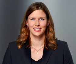
Drolz, Isabella

Drolz, Isabella
Vice President Product Marketing
Comet Yxlon GmbH

Drolz, Isabella

Abstract
The global demand for high-end computing power driven by smartphones, IoT applications, High-performance computing, and new mobility applications is constantly rising while facing miniaturization demands. The semiconductor industry is all about identifying and solving these challenges and thereby, yield and process control is core for foundries and its importance increased even more through the introduction of advanced packaging.In today’s environment two things can be observed. One, prototyping and verification costs exponentially increase while node sizes decrease. Two, a change from typical inspection methods like optical or FIB-SEM to advanced non-destructive inspection techniques like X-ray inspection.Ultimately advanced packaging companies seek non-destructive automated inspection tools which are fast enough to provide value within their production processes, increase yield and reduce waste at an early stage. This presentation will give an overview on how X-Ray and CT inspection can provide value-added data and information for exactly that.

Biography
Isabella Drolz is the Vice President Product Marketing at Comet Yxlon, which is the industrial X-ray & CT inspection system division of Comet. Comet Yxlon provides X-ray & CT inspection solutions for R&D labs & production environments, especially for Semiconductor customers to enhance their productivity. In her role she is responsible for product management, business development, global application solution centers and marketing at Comet Yxlon. Isabella has next to her industrial engineering education, a Bachelor of Science in International Business Administration and a MBA degree from Southern Nazarene University in Oklahoma City, USA. She has held several management positions in the mechanical and plant engineering industry driving market-oriented product development.

Advanced Packaging Conference
Comet Yxlon International GmbH Comet Yxlon International GmbH Driller, Christian
Zero defects matter | The Power of Xray in Advanced Packaging
Driller, Christian

Driller, Christian
Vice President R&D
Comet Yxlon International GmbH

Driller, Christian

Abstract
The semiconductor industry faces numerous challenges in the development and manufacturing of advanced packages. From a technical standpoint, these challenges include miniaturization, thermal management, and interconnect technologies. From a market perspective, challenges arise from higher production mixes due to application-specific integrated circuits (ASICs) and customers' intolerance for failures, particularly in critical automotive applications. These challenges have resulted in constantly increasing costs for designing and manufacturing ICs.Consequently, the industry is adopting two key approaches. Firstly, it is embracing lights-out manufacturing, which involves fully automated factory operations that offer increased productivity, improved repeatability, and consequently, enhanced quality. Secondly, new testing strategies are being implemented to provide data for advanced process analytics, enabling a shift from reactive to predictive actions. These strategies aim to improve traceability, yield, and overall operational efficiency.In the monitoring of interconnect characteristics such as diameter, height, co-planarity, and bump quality, inspection tools play a crucial role. Advanced X-ray technology, in particular, holds significant potential in driving the development of defect-free advanced packaging solutions through identifying root causes of failures.

Biography
Since 2020, Christian Driller has held the position of Vice President of Research and Development at Comet Yxlon, where his team spearheaded the development of cutting-edge x-ray and CT inspection solutions. Under his leadership, he has successfully established an agile R&D organization with a strong customer-centric focus, fostering a passionate and results-oriented team.Prior to his current role, Christian Driller assumed the position of Vice President of Business Excellence at Comet Yxlon in 2017. In this capacity, he played a pivotal role in driving the professionalization efforts across all functional areas of the company.Christian's professional journey commenced in 2012 within the automotive industry, where he served as a Business Consultant at Porsche Consulting. His primary focus was on optimizing and restructuring R&D departments within both automotive manufacturers and suppliers, delivering impactful results.Christian Driller holds a Master's degree in Finance from ESB Reutlingen University and a Bachelor of Engineering from Baden-Wuerttemberg Cooperative State University. Notably, during his undergraduate studies, he collaborated closely with Dr. Ing. h.c.F. Porsche AG, serving as his cooperating company.

Future Disruptions
D To top
D-SIMLAB Technologies D-SIMLAB Technologies Lendermann, Peter
Squeezing More Wafers out of a Fab: Can this be Done without Driving Cycle Times Through the Roof?
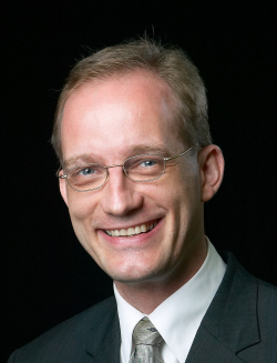
Lendermann, Peter

Lendermann, Peter
Chief Business Development Officer
D-SIMLAB Technologies

Lendermann, Peter

Abstract
Despite the current dip in global IC demand in some areas, industry leaders are optimistic about mid- and long-term growth prospects in semiconductor manufacturing which is also illustrated by the large number of new wafer fabrication facilities that are already under construction or being planned across the globe.In this setting, optimisation of factory capacity – with the objective to squeeze even more wafers out of existing fabs – will continue to be a critical challenge. To achieve this, powerful techniques to determine fab load mixes that are able to maximise wafers out – or better revenue, or even much better margin – with existing capacity are essential. At the same time, because of the complex operating curve of a wafer fab it is important to precent cycle times from going through the roof to make sure that delivery performance to customers does not suffer. In an environment with fast-changing customer demand and product mixes, as well as frequent commissioning of new equipment this is not an easy task at all.How such load mix optimisation can be achieved through a combination of static and dynamic (simulation-enabled) capacity models and powerful yet intelligent optimisation techniques will be showcased in this presentation. Enhancement of the wafer out potential by a double-digit percentage without exceeding operationally feasible equipment utilisation limits and without compromising cycle time has been demonstrated with multiple semiconductor manufacturing companies.

Biography
Peter Lendermann is a Co-Founder and the Chief Business Development Officer of D-SIMLAB Technologies, a Singapore-headquartered company providing simulation-based decision support solutions to Semiconductor Manufacturing companies. Prior to this he worked at the Singapore Institute of Manufacturing Technology where he led related R&D activities until spinning them off into D-SIMLAB. Peter has been engaged in the field of production logistics, supply chain management and related decision support technologies and solutions since the early 1990’s. He holds a PhD in Physics from Humboldt University in Berlin (Germany) and an MBA in International Economics and Management from SDA Bocconi in Milan (Italy).

Fab Management Forum
DAS Environmental Experts GmbH DAS Environmental Experts GmbH Raithel, Stephan
Coming Soon
Raithel, Stephan

Raithel, Stephan
COO Gas Treatment and General Manager US
DAS Environmental Experts GmbH

Raithel, Stephan

Abstract
Coming Soon

Biography
Stephan Raithel joined DAS in 2016 and since then holds the position of the COO Gas Treatment. In his position he is overseeing all aspects of DAS’ gas treatment products, such as development, engineering, product management, procurement, customer care and production. In parallel he also acts as General Manager for the US subsidiary.From 2007 until 2016 he was working for SEMI, the global semiconductor equipment and materials association, where he held various positions within the association – from operations management, SEMI standards and PV Roadmap program to the role of the Managing Director of SEMI Europe.Before his start in the semiconductor industry, he was employed as a project manager in the financial ,creative services and consumer goods industry.

Future Disruptions
DigitalTwin Technology GmbH DigitalTwin Technology GmbH Tomar, Rahul
Digital Twin Software for Finite Element Analysis.
Tomar, Rahul

Tomar, Rahul
Managing Director
DigitalTwin Technology GmbH

Tomar, Rahul

Abstract
Finite Element Analysis (FEA) has long been a pivotal tool in engineering and design, enabling the simulation of complex physical systems. However, as industries evolve towards greater complexity and integration, there is an increasing need for advanced software solutions that can enhance the capabilities of FEA. This presentation introduces the concept of Digital Twin Software for Finite Element Analysis (DT-FEA), a transformative approach that harnesses the power of digital twins to elevate the accuracy, efficiency, and comprehensiveness of FEA simulations.DT-FEA bridges the gap between physical and digital realms by creating a virtual replica of a physical system. This digital twin faithfully captures not only the geometry but also the material properties, boundary conditions, and dynamic behavior of the real-world counterpart. It leverages real-time data integration, AI-driven analytics, and multidisciplinary modeling to continuously update and refine the digital twin's representation, ensuring its fidelity to the evolving physical system.Key advantages of DT-FEA include:1. Real-time Monitoring and Predictive Analysis: DT-FEA allows engineers and analysts to monitor the performance of physical systems in real time. By continuously comparing the digital twin's behavior to the actual system, deviations and anomalies can be detected early, facilitating predictive maintenance and reducing downtime.2. Multidisciplinary Integration: DT-FEA enables the integration of multiple simulation domains, such as structural, thermal, fluid, and electromagnetic analysis, within a single platform. This holistic approach provides a comprehensive view of system behavior and interactions.3. Optimization and Design Exploration: With DT-FEA, designers can explore a vast design space efficiently. Parametric studies and optimization algorithms can be applied to the digital twin, accelerating the development of innovative and efficient solutions.4. Collaborative Decision-Making: DT-FEA supports collaborative decision-making by providing a common platform for engineers, designers, and stakeholders to interact with and analyze the digital twin. This fosters cross-functional collaboration and informed decision-making.5. Reduced Cost and Risk: By enabling a deeper understanding of system behavior and performance, DT-FEA reduces the need for costly physical prototypes and mitigates the risk of unexpected failures or performance issues in real-world applications.

Biography
Rahul Tomar is a distinguished mechanical, civil, and software engineer with over 23 years of extensive experience in the field of engineering and technology. He is most notably recognized as the Co-Founder of DigitalTwin Technology GmbH, a groundbreaking company at the forefront of the digital twin revolution in the engineering and construction sectors.Rahul's profound understanding of mechanical and civil engineering principles, coupled with his expertise in software development, has played a pivotal role in the success of DigitalTwin Technology GmbH. He has spearheaded the development of innovative software solutions that bridge the gap between the physical and digital worlds, revolutionizing how engineers and designers approach their work.Through his leadership, DigitalTwin Technology GmbH has enabled organizations across the globe to harness the power of digital twins for real-time monitoring, predictive analysis, and collaborative decision-making. These advancements have not only improved efficiency in engineering and construction projects but have also significantly reduced costs and risks associated with complex ventures.Rahul Tomar's relentless pursuit of excellence and his unwavering dedication to pushing the boundaries of technology have left an indelible mark on the engineering and software development industries. His vision for the future of digital twin technology continues to drive innovation and transformation, making him a respected figure in the global engineering community.

EU DIGITAL FUTURE FORUM
E To top
Edwards Edwards Jones, Chris
The Challenge to Reduce Emissions during a Period of Growth
Jones, Chris

Jones, Chris
Environmental Solutions Business Development Manager
Edwards

Jones, Chris

Abstract
The establishment of the Semiconductor Climate Consortium underscores the semiconductor industry's unwavering dedication to confronting both its unique and shared challenges concerning greenhouse gas emissions. Given the longevity of many of these gases in our atmosphere, their management is crucial and will also gain heightened significance over time. We will examine releases from our industry using both a top-down and bottom-up approach and juxtapose them with efforts from other sectors. Central to our discussion will be emissions management strategies that resonate with the Consortium’s emphasis on holistic collaboration across the value chain, bolstered by the active involvement of myriad external stakeholders.

Biography
With a Ph.D. in chemistry and nearly four decades of dedication to Research and Development and Environmental Protection, Chris has been at the forefront of creating solutions for industries ranging from semiconductor and nuclear to military and pharmaceutical. He's crafted methods to keep our air and water clean and is currently Edwards' Environmental Solutions Business Development Manager. Always eager to share his knowledge, Chris is passionate about helping fab owners grasp their operations' local and global environmental impacts. He's genuinely committed to a greener future!

imec ITF
Edwards Edwards Pelissier, Christine
Sustainability through Inclusion: how Surveys (Insights) + Analysis Support our Understanding of Generational Expectations
Pelissier, Christine

Pelissier, Christine
General Manager, Customer Center EMEA
Edwards

Pelissier, Christine

Abstract
Join us to gain valuable insights into how Edwards Semiconductor Divisions are leveraging data-driven strategies to promote inclusion, diversity, and unity within the organization. Discover how this approach not only bridges generational gaps but also reinforces the shared vision of a workplace that inspires and supports every individual.In the dynamic landscape of the semiconductor industry, fostering an inclusive and diverse workplace is not just a commitment but a strategic imperative. Edwards Semiconductor Divisions, conduct a employee survey every two years to continuously improve its work environment. This year, a new dimension was added to the survey - Inclusion and Diversity. In this presentation, Christine will delve into the insights derived from this survey, showcasing how data can drive a meaningful dialogue and enhance employee engagement.One of the standout revelations from the survey is the exploration of generational differences. By dissecting the data across generations, Christine uncovered surprising and positive trends that challenge conventional wisdom. She will shed light on the distinct priorities of different generations within the organization, offering compelling conclusions and actionable adjustments that can be considered to nurture a workplace that caters to all.Beyond the generational divide, Christine's presentation will also explore the fundamental similarities in what employees across all generations seek and need from their workplace. By identifying these common threads, Edwards Semiconductor Divisions aim to create a workplace culture that fosters inclusivity, enhances diversity, and, most importantly, empowers every employee to thrive.

Biography
Christine has a proven track record of hiring, developing and managing high performance teams which consistently create superior value. She has over 30 years’ experience successfully growing markets and customers in a high-tech environment and has broad international experience building networks in North America, Europe, and Asia. Prior to joining Edwards in 2018, Christine has held senior strategic marketing positions, business development, operations and applications roles with Applied Materials, KLA-Tencor and Soitec.

Future of Work
Edwards Edwards Lauwers, Koen
Sustainability through Innovation: a Superior Technology Story
Lauwers, Koen

Lauwers, Koen
President Semiconductor Division
Edwards

Lauwers, Koen

Abstract
Semiconductor sales are powering towards a staggering 1 billion USD in the next decade and we all want to be around to enjoy the results – quantum computing, smart healthcare, robotic servants, autonomous vehicles … space travel(!) We find ourselves on the cusp of remarkable growth and we are faced with a unique opportunity too important to pass up. As Edward’s technology influence expands from the sub fab to chamber solutions to long-term after-service – our approach to sustainability is evolving too: our pursuit of superior technology must, necessarily, be intrinsically interwoven with sustainable innovation. Our Science Based Targets initiative (SBTi) commitments serve as a constant and resounding reminder, urging us to ensure that our explorations of novel approaches lead us to advancements that are not just distinct, but genuinely superior. Lower power; smaller footprint; non-fuel products; minimising and recycling resources and raw materials; product longevity; predictive maintenance programmes; and repairability [NEW] are all front and centre as we develop new products and approaches. We are reaffirming our commitment to both environmental consciousness and sustainability with real-world measures across the organization – embedding checks and balances not just in our R&D but in all our business processes. Leveraging principles of sustainability, we aim to drive a revolution characterized by longevity and responsibility, ensuring that our growth is always aligned with the environment and society at large. There will be some step changes but our journey is a continuous pursuit of incremental improvements. Some seemingly modest strides will deliver an enduring positive impact – and deliver transformation through superior technology.

Biography
Koen Lauwers, joined Atlas Copco in 1997, joining as a Calculation Engineer and has since then built a successful career in the Group, including international assignments in the United States and Germany.Koen joined Edwards in 2014 following the acquisition by Atlas Copco, taking the role VP of Marketing and focusing on the industry segment and implementation of synergies. In 2017 he was appointed President of the Industrial Vacuum division, before being announced as the new President of the Semiconductor division on March 30, 2023.Koen holds a Master’s Degree in Electro-Mechanical Engineering from the University of Leuven in Belgium and an MBA from the Antwerp Management School in Belgium.

CEO Summit
Einnosys Technologies Einnosys Technologies Thakkar, Nirav
Adding Automation (SECS/GEM) Capabilities on Legacy Equipment
Thakkar, Nirav

Thakkar, Nirav

Einnosys Technologies

Thakkar, Nirav

Abstract
OverviewSEMI's SECS/GEM standards have become the de-facto communication protocol for semiconductor equipment to interface with factory systems. These standards prevent human errors in selecting incorrect recipes and enable equipment performance monitoring. However, many smaller fabs and assembly, test, and packaging factories still have legacy equipment without SECS/GEM capabilities. Adding SECS/GEM functionality to such equipment has posed challenges due to discontinued OEM support and expensive upgrades. This hinders factories from achieving improved yields, cycle times, and automation benefits.Plug-n-Play SECS/GEMTraditionally, SECS/GEM capability must be purchased from the OEM and integrated at the source code level. Some companies offer "black box" solutions, but they have limitations and potential side effects. A better approach is using equipment PC peripherals to add SECS/GEM capabilities. Data can be extracted from the equipment's controller GUI using computer vision and AI technologies, and remote control commands can be sent through the equipment PC's mouse and keyboard interface.Enhanced Automation CapabilitiesThe peripheral-level approach allows for safer integration without side effects. Additionally, AI/ML and computer vision technologies can enhance automation capabilities beyond SECS/GEM standards. This includes sending images of wafer measurements or inspections, enabling Robotic Process Automation (RPA) on the equipment, and allowing remote desktop access to equipment without a network connection. Implementing this approach overcomes challenges associated with legacy equipment and unlocks automation benefits.

Biography
Nirav Thakkar is a highly accomplished professional with a diverse background in software engineering and business administration. He received his Bachelor of Computer Engineering degree from the University of Mumbai, India in 1994, and later pursued an MBA from Pepperdine Graziadio Business School in Los Angeles, CA, which he successfully completed in 2012.He has gained valuable experience throughout his career, working in various roles and organizations:Software Engineer at Symmetric Multiprocessing (1995 - 1996):During his one-year tenure at Symmetric Multiprocessing, He contributed as a Software Engineer, utilizing his technical skills to develop software solutions.Project Lead at Contech Software Ltd (1996 - 1999):He took on the role of Project Lead at Contech Software Ltd, where he demonstrated leadership abilities and successfully managed projects for a span of three years.Senior Factory Automation Engineer at Conexant (1999 - 2002):In this position, He focused on factory automation engineering, utilizing his expertise to optimize and improve automation processes during his three-year tenure with Conexant.Software Development Manager at Oraxion (2002 - 2003):As a Software Development Manager at Oraxion, He assumed responsibilities for managing software development projects, overseeing teams, and ensuring successful project outcomes.Project Lead at Wonderware Invensys (2004 - 2006):He served as a Project Lead at Wonderware Invensys, where he led and coordinated projects for two years, leveraging his skills to deliver high-quality software solutions.VP - GLA - LIG - Ventura County at itSMF (2010 - 2011):He held a leadership role at itSMF as VP - GLA - LIG - Ventura County, contributing to the organization's goals and initiatives during his one-year tenure.Senior Engineering Manager (Factory Automation/Software Development) at Skyworks Solutions Inc (2006 - 2013):During his seven-year tenure at Skyworks Solutions Inc, He played a crucial role as a Senior Engineering Manager, focusing on factory automation and software development. He demonstrated his leadership abilities and contributed significantly to the company's success.In addition to his professional roles, He is also an entrepreneur and a founder. Since 2013, he has been the Founder and President of eInvenSys Technologies, a company that specializes in providing innovative technological solutions. Moreover, He is also the Founder and President of eInnoSys Inc, a company he established in 2013, which focuses on driving innovation in the industry.With his extensive experience and entrepreneurial spirit, He continues to make valuable contributions to the field of software engineering and technology.

Innovation Showcase (pre-recorded)
ElectraMet Lippert, Cameron
Building A More Sustainable CuCMP Process: Selective Copper Removal & Recovery

Lippert, Cameron

ElectraMet

Abstract
Challenge: (1) Current Cu-CMP processes are unsustainable due to the large amounts of waste copper that end up in the wastewater, millions of kgs per year combined (2) Complicated wastewater matrix makes treatment to remove copper to meet discharge compliance burdensome and expensive, (3) Evolving Cu-CMP chemistries that produce copper laden wastewater that is unable to be treated with conventional treatment solutions. Urgency: (1) Pressure to meet ESG targets of recycling water and waste as well as decarbonization, (2) Copper demand outpacing supply and Cu-CMP produces a large amount of recoverable copper waste, (3) Increasing cost to treat more complex CMP slurry matrices, (4) Current solutions for treatment rely on chemistry or consumable media which are subjected to an unpredictable supply chain.Solution: Electrochemical device (chemical-free) to selectively remove AND recover copper form complex streams without damaging the slurry mixture.ElectraMet® is an electrochemical system for targeted metals removal from process and wastewater streams. This system uses an automated process to treat CuCMP rinse/wastewater directly at the customer site by removing and recovering Cu as high purity metal sheets while achieving discahrge limits (sub mg/L) in the wastewater. This process leaves the rest of the slurry mixture in tact potentially allowing the slurry mixture to be reused. By electrochemically recovering copper, ElectraMet has proven to be a simple and efficient on-site solution for CuCMP wastewater treatment, even in the presence of other chemicals. ElectraMet does not rely on chemicals for its treatment, the overall operation is simpler, and the footprint is much smaller, than other on-site options.ElectraLink™ is an assurance program that provides an additional layer of support by allowing ElectraMet engineers to monitor your system on your behalf in real time. ElectraLink uses a secure cellular connection to run remote diagnostics, send daily system reports, and can protect you from costly downtime. With ElectraLink, historical trends and changes to the water treatment process can be tracked in real-time including monitoring of alarm codes, tank levels, pressure drops, valve positions, pH, and ElectraMet cartridge diagnostics. The ability to actively monitor these process conditions means you can avoid possible upset conditions that result in tank overflows, lack of proper water treatment or impurity removal, or flow-limiting pressure conditions.

Biography
Dr. Cameron Lippert is the Co-Founder, and Chief Innovation Officer at ElectraMet. Dr. Lippert is a serial entrepreneur with over a decade of experience in developing innovations and bringing them to market. In this role, he is responsible for identifying and developing new industry applications for ElectraMet. He is also in charge of identifying key product development needs to solve evolving industrial process water and wastewater challenges. Prior to becoming an entrepreneur, Cameron managed multimillion dollar R&D and technology development & demonstration projects at the Center for Applied Energy Research at the University of Kentucky ranging from carbon capture to new battery chemistry.Dr. Lippert received his BS in Biochemistry from Eckerd College and a Ph.D. in Inorganic Chemistry from the Georgia Institute of Technology, and has more than 50 publications and patents in the field.

Innovation Showcase (pre-recorded)
Elmos Semiconductor AG Elmos Semiconductor AG Montino, Ralf
It is all about Cost of Test? New Duties for Packaging and Test
Montino, Ralf

Montino, Ralf
VP PLI
Elmos Semiconductor AG

Montino, Ralf

Abstract
In the past, the processes “Wafer Sort”, “Assembly” and “Final Test” were considered as more or less independent processes with limited duties: Assembly should cover the silicon and the two test processes took care about the functionality of the product. Efficiency increase results from reducing test effort and increasing the parallelism of the test.Today, more and more of the products are customized during the test. This includes flashing customer specific software as well as adjustments at sometimes several temperatures. A more integrated view on these three different steps is necessary. Moreover, there are new demands to the machines. In addition to that, increasing of parallelism is very limited by the handling systems available on the market.

Biography
Study of physics in Dortmund and Aachen (high-energy physics).PHd in Engineering from the University of Siegen ( Knowledge Based Systems and Knowledge Management )With Elmos since 1990. - Started working for Elmos as a developer of test programs for the automatic electrical test of products.From the middle of the 90's development of the IT at Elmos. (There was actually nothing like that before - you can hardly imagine it today ...)Besides the office IT from the beginning, the integration of the manufacturing processes into the IT structures was a focus.After many years of responsibility for IT: Establishing a new organizational structure taking care about test program development, product engineering and assemblyThe core topics are:Broadening the supply chain, growth at the OSATSEngineering EfficiencyAnd, for shure, COT

Advanced Packaging Conference
Entegris Amade, Antoine
Chairman of the session
Amade, Antoine

Amade, Antoine
President, EMEA Region
Entegris

Abstract
Due to its properties of wide band gap and high thermal conductivity, Silicon Carbide is a compelling choice for an increasing number of semiconductor power applications in a multitude of growing industries. Higher voltages, higher frequency of operation and overall efficiency gains are obtained. Specifically for e-mobility, size and weight for a given performance, as well as enhanced charging speed, can be significant benefits over conventional silicon.However,the SiC industry faces several important challenges, roughly charactered as :•Quality: reliability demanded from the automotive sector is severe and there is still room to improve the maturity of processing SiC.•Cost of Production: achieving high and consistent yieldsis challenging in the fab and the supply chain.•Capacity: the increasing demand is leading to capacity constraints in SiCsubstrate manufacturers and fabs.The session will offer the opportunity to get insights from senior business speakers with the objective to trigger meaningful collaboration along the supply chain and the entire ecosystem. Enjoy!

Biography
Mr. Amade joined Entegris in 1995 as an application engineer in its semiconductor business. Today, he is the President of the Europe and Middle East (EMEA) region as well as the VP of sales for the Microcontamination Control division focused primarily on growing the semiconductor business in North America, Europe and the Middle East through market strategies and the management of sales. For more than 25 years, Mr. Amade has held leadership positions at Entegris in gas microcontamination market management, strategic account management, and regional sales management. Mr. Amade has a degree in Chemical Engineering from ENS Chimie Lille and is a member of the SEMI Electronic Materials Group, the Global Automotive Advisory Council for Europe (GAAC) and the Platform for Automotive Semiconductor Requirements Along the Supply Chain (PASRASC).

Entegris
Entegris Entegris Mahadev, Niraj
Meeting the SiC Gold Rush with Entegris Capabilities
Mahadev, Niraj

Mahadev, Niraj
Vice President, Advanced Planarization Solutions (APS) Division
Entegris

Mahadev, Niraj

Abstract
Entegris leads the way in the design and manufacturing of dedicated SiC consumables, including CMP slurries, post CMP cleans, and pads. Our products are meticulously engineered for high-volume production, catering to the growing demand in the industry.Our versatile products can be utilized across a wide range of new and existing OEM tools, such as single, double, and batch polishing equipment. By incorporating our slurries, these tools experience improved thruput efficiencies while simultaneously reducing wafer level defects and scratches.Post CMP cleaning of wafers is of utmost importance, ensuring the removal of particles and metal contaminants before the epitaxial process. Our post CMP cleans are specifically developed to address this challenge while maintaining the performance of CMP pads and tool sets through effective cleaning solutions.Lastly, Entegris possesses cutting-edge cleanroom facilities, enabling us to conduct in-depth studies, analysis, and testing of pad/slurry interactions. This capability allows us to develop next-generation slurries and cleans, particularly as the industry transitions from 6" to 8" wafer sizes.The focus of this presentation is to showcase compelling data on the performance of Entegris' SiC consumables across various toolsets, addressing both current and future industry requirements.

Biography
Niraj Mahadev is an esteemed professional with a proven track record as a leader in the semiconductor industry since 1999. With extensive experience in the TDK Group of Companies, he has successfully held diverse roles in multiple countries across Southeast Asia and the USA. Throughout his career, Niraj has excelled in research and development (RD), new product introduction (NPI), yield optimization, and operations management. Notably, he demonstrated exceptional leadership skills while overseeing a large-scale manufacturing facility. Additionally, Niraj served as the managing director at BASF MicroChemicals, where he exhibited expertise in managing PCMP cleans and polishing/lapping slurries for the processes within the Hard Disk Drive Industry.Niraj Mahadev's career has been marked by remarkable achievements and notable milestones. His contributions have been instrumental in driving industry advancements, including the successful adoption of the first Apple iPod hard disk drive. He also orchestrated the seamless transfer of high-volume manufacturing for hard-drive products from the United States to Singapore, optimizing operational efficiency and global supply chains. His impactful career highlights his ability to lead and deliver groundbreaking solutions in the semiconductor and storage industries.Within Entegris, Niraj Mahadev leverages his wealth of experience and deep-rooted passion to drive advancements in the realm of advanced planarization solutions. His primary objective revolves around the development of specialty chemical products that seamlessly integrate chemistry and processes. By doing so, he aims to tackle the persistent challenges of enhancing performance, yield, and reliability in the storage, optical, and semiconductor industries. Through his dedication and expertise, Niraj contributes to shaping the future of these sectors by spearheading innovative solutions that optimize processes and elevate overall industry standards.

Entegris
European Association of Career Guidance European Association of Career Guidance Mavromoustakou, Maria
ECoVEM project: Path to certification and recognition
Mavromoustakou, Maria

Mavromoustakou, Maria
Project Manager
European Association of Career Guidance

Mavromoustakou, Maria

Abstract
The ECoVEM project is a collaborative effort that unites vocational education and training (VET) centers, polytechnics, industrial associations, and social partners. Its aim is to establish a European Cooperation platform of Vocational Excellence in Microelectronics to address various challenges, including digitalization, artificial intelligence, green technologies, gender equality, and the integration of migrants. ECoVEM leverages and complements the strengths of national VET systems, particularly in countries with more advanced VET programs, while also supporting less advanced regions in their journey towards achieving VET excellence. The project adopts innovative instructional methods that promote lifelong learning, encompassing both hard and soft skills, using theoretical models based on ecosystems and performance support systems. The ECoVEM consortium developed the path to certification and mutual recognition of the ECoVEM curriculum and training, which consists of six distinct courses covering microelectronics and its applications, with a total of thirty-three modules. All available courses can be accessed on the project's official website, www.ecovem.eu. The project provides a flexible path, serving as an open methodology for planning and implementing the certification and recognition process.

Biography
Maria Mavromoustakou is a Project Manager at the European Association of Career Guidance in Cyprus, where her primary role encompasses project implementation and management. Her professional journey commenced at the University of Nicosia, where she held the position of Environmental Researcher. During this tenure, she made significant contributions to the preparation of numerous European-funded environmental projects. Subsequently, she worked as a Project Manager at the Cyprus Sustainable Tourism Initiative, a nonprofit organization in Cyprus. In this capacity, her core responsibilities included crafting project proposals and overseeing projects related to sustainability initiatives. Maria then advanced her career as a Training and Development Officer and Erasmus Officer at the University of Nicosia. Her academic qualifications include an M.Sc. in Ecotourism from Edinburgh Napier University (Scotland) and a B.Sc. in Environmental Management from the University of Hertfordshire (UK).

Future of Work
EV Group EV Group Varga, Ksenija
Optimization of Advanced Packaging Process: Concept of Maskless Dual–Layer Lithographic Patterning
Varga, Ksenija

Varga, Ksenija
Business Development Manager
EV Group

Varga, Ksenija

Abstract
The integration of advanced packaging features in heterogeneous integration, 3D stacking, and miniaturization of electronic devices is enabled by FO WLP. It offers several benefits, including improved electrical performance, reduced form factor, and enhanced thermal dissipation vs. conventional packaging technologies. The cost–efficient solution to the industry established dual–damascene process in the interconnect formation was investigated in the present paper in relation to the FO WLP application. For this purpose, the concept of maskless exposure patterning of the novel dielectric materials by using two exposure dose levels was set in the DoE.The lithographic patterning was performed by dual–dose exposure of VIA and RDL traces using a single coating and development step without intermediate alignment. The objective was to achieve low resolution, low dielectric layer thickness having half–thickness of the first layer in the dual exposed patterns. A newly developed, low–temperature cure positive tone polybenzoxazoles (PBO) dielectric is cured at about 200 °C and thus is compatible with epoxy materials used in FO WLP packages.The low–temperature cure dielectric was also developed for markets like MRAM, RF, MEMS, and backside RDL applications where the base substrate, other materials, or the device packages themselves are temperature sensitive and require a low–cure dielectric material.At first, an understanding of dose dependency on the dielectric penetration depth in dual–layer exposure needed to be proven. Maskless exposure technology offers a simple exposure dose/wavelength/focus matrix. The parameters can be easily adjusted via recipe enabling efficient process evaluation. The contrast curve proved the linear behavior of exposure dose vs. removed thickness layer after the development. By patterning with the most optimal dual–exposure parameters, the resolution 3.8 µm (via within via opening), min. dual–layer thickness of 8 µm (first layer thickness 4 µm) after cure was proven by SEM images and stylus profile measurement. The spectral reflectance images reveal uniform film thickness (FT) distribution after spin coating, while the FT non–uniformity increased after the cure and the development processes.In conclusion, the newly established concept can support continuous efforts of the BEOL semiconductor industry in the total cost–of–ownership optimization.

Biography
Ksenija Varga is Business Development Manager at EV Group with Head Quarter in Austria, where she is focusing on new application development for maskless exposure technology, primarily in advanced packaging and heterogenous integration. Besides business development, Ksenija is involved in strategic projects working on new lithography equipment for next-generation devices. Prior to EV Group, Ksenija was working at FujiFilm Electronic Materials. She holds a doctorate degree in Chemistry from the University of Innsbruck in Austria and has experience in R&D project management and account management.

Advanced Packaging Conference
Evatec Evatec Rettenmeier, Roland
Opening Remarks
Rettenmeier, Roland

Rettenmeier, Roland
Senior Product Marketing Manager
Evatec

Rettenmeier, Roland

Abstract
Coming Soon

Biography
Roland Rettenmeier qualified as a Mechanical Engineer in 1997 and completed his MBA studies at Vienna, Austria in 2005. Roland extended his education through other international courses and programs since that time (e.g. Six Sigma Program with AT&S and Nokia; Innovation Technology Leader at Stanford University).Roland has worked in the field of Electronics and Semiconductor manufacturing since 2001, managing multiple international projects. After joining Evatec in 2016 as Senior Product Marketing Manager (PMM) within the Business Unit for Advanced Packaging, he focused on business development for Panel Level Packaging where Evatec has now become the recognised market leader for thin film technology solutions. Since 2020 he has also supported development of Evatec’s wafer level packaging solutions business.In addition to his market and customer responsibilities, Roland represents Evatec in the Panel Level Packaging consortium of Fraunhofer IZM Berlin, in the Packaging Research Center at Georgia Tech, USA and in the Panel Level Packaging Consortium at the NCAP in Wuxi, China.

Advanced Packaging Conference
EVG EVG Brandl, Elisabeth
Manufacturing next generation power devices – how temporary bonding allows wide bandgap power devices to go vertical.
Brandl, Elisabeth

Brandl, Elisabeth

EVG

Brandl, Elisabeth

Abstract
Wide bandgap power devices are experiencing a strong growth, especially SiC and GaN technologies are in the front seat. Reason for that growth are mainly electronic vehicles and renewable energy but also the general need for efficient, low loss power conversion. However, both SiC and GaN still face challenges. For SiC the transition to 200mm wafers is still not implemented in the extent to satisfy industry’s demand. GaN is facing technological challenges where only lateral devices with a therefor limited breakthrough voltage are commercially available yet. A novel approach is the transition to vertical devices where a higher breakthrough voltage and therefore wider application window can be expected.For better thermal management temporary bonding was already implemented for lateral GaN power devices, but for vertical GaN power devices grown on foreign substrates, temporary bonding is an essential and critical block in the manufacturing chain.SiC power devices on small wafer sizes not necessarily need temporary bonding as mechanical support during thinning because of SiC’s robust nature. Going to 200 mm wafers temporary bonding is also a necessary process enabling thinning and backside processing.In the presentation the different process flows for wide bandgap power devices with their unique challenges will be discussed and an outlook on the manufacturability on future devices will be given – a focus will be the process compatibility of the temporary bonding during growth substrate removal for GaN power devices and thinning for SiC power devices as well as metal contact formation will be reviewed.This project has received funding from the ECSEL Joint Undertaking (JU) under grant agreement No 101007229. The JU receives support from the European Union’s Horizon 2020 research and innovation program and Germany, France, Belgium, Austria, Sweden, Spain, Italy.

Biography
Elisabeth Brandl is product marketing manager at EV Group for temporary and adhesive bonding and works for EVG since 2014. She holds a Master degree (DI) in technical physics from the Johannes Kepler University Linz specialized on nanoscience and - technology. During her master thesis at the institute of semiconductor and solid state physics she gained experience for semiconductor processing and nanofabrication.

Innovation Showcase (pre-recorded)
F To top
Flexciton Ltd Flexciton Ltd Potter, Jamie
Topic to be confirmed soon
Potter, Jamie

Potter, Jamie
Co-founder and CEO
Flexciton Ltd

Potter, Jamie

Abstract
Abstract to be delivered soon

Biography
Jamie Potter, CEO and Co-founder, FlexcitonJamie is passionate about solving the hardest industrial problems. For the past 10 years, he has been developing optimisation solutions for various sectors, with a focus on semiconductor manufacturing. As an entrepreneur at heart, after spending a few years working in an industrial consultancy, Jamie co-founded Flexciton in 2016. He was initially directly involved in developing and implementing the first release of Flexciton scheduling software at the Seagate Springtown wafer fab. Along with his role as the company CEO, Jamie leads the commercial and operations teams. Over the past 7 years, Jamie has worked on over a dozen operational improvement projects with various semiconductor manufacturers. Jamie is a smart manufacturing enthusiast with an ambition to bring new technology to the semiconductor industry to enable new levels of efficiency.Jamie has graduated with honours in MMath from Oxford University, UK. In 2018 he was featured in Forbes' “30 under 30 list”.

Fab Management Forum
Fraunhofer-Gesellschaft Fraunhofer-Gesellschaft Stephan, Jörg
Coming Soon
Stephan, Jörg

Stephan, Jörg
Project Manager and Research Coordinator
Fraunhofer-Gesellschaft

Stephan, Jörg

Abstract
Coming Soon

Biography
Coming Soon

Future of Computing
Fraunhofer EMFT Fraunhofer EMFT Kutter, Christoph
Topic Coming Soon
Kutter, Christoph

Kutter, Christoph
Executive Director
Fraunhofer EMFT

Kutter, Christoph

Abstract
Coming Soon

Biography
Coming Soon

Future of Computing
Fraunhofer FMD Töpper, Michael
A European 3D Heterogeneous Integration Pilot Line – a Leap ahead to Achieve Technology Leadership

Töpper, Michael
Senior Expert Heterointegration Research Fab Microelectronics Germany (FMD)
Fraunhofer FMD

Abstract
The digital transformation of society and economy creates an increasing demand to transfer, process and store vast amounts of data generated in the context of technologies such as artificial intelligence (AI) and the Internet of Things (IoT). Therefore, future electronic systems like autonomous systems using high-performance computing (HPC) and edge computing systems, sensor-integrated systems and bio-integrated devices will require more and more functions that cannot be managed by a single chip, even if advanced system on chip (SoC) concepts are used. Therefore, advanced 3D heterogeneous integrated systems are the next step of evolution of the IC scaling. To support this a roadmap for required technology developments in heterogeneous integration has been defined by a joint working group of FMD and industry partners with a horizon of 2030 and beyond.It includes lithographical scaling that supports sub µm hybrid bonds pitches. The thermal management of extreme heat dissipation and topological limitations by STCO measures, new materials and new cooling methods. Comprehensive testing of dies to achieve an economically reasonable yield in a complex heterogeneous integration process containing a higher number of dies. To improve the processes and to understand failure mechanisms an appropriate failure analysis has to be codeveloped together to address fails in 3D stacks. Without the possibility to manufacture parts throughout a complete assembly process the full assessment of the impact of these topics is not possible. By looping in wafer or dies of leading-edge CMOS or special technologies like GaN from industry partners or collaborating research and technology organizations advanced processor devices can be realized through an innovative pilot line. Such a pilot line also allows to explore an automotive grade technology along with other industrial applications requiring high robustness. Together with the planned investments into Silicon frontend manufacturing and assembly in Europe as announced e.g. by Intel the heterogeneous integration pilot line at the chip, package and organic substrate level plays a key role to excel the position of Europe as hub for assembly and test.The paper will be presented together with Intel and Siemens EDA.

Biography
Michael Töpper studied chemistry at the University of Karlsruhe and received his doctorate in materials science from the Technical University of Berlin. He has been working in the field of assembly and connection technology for microelectronics since 1994, initially at the TU Berlin, then as a group leader at Fraunhofer IZM including a year at the University of Utah as an assistant professor and until 2021 as a business developer for the entire IZM. Today he represents the Research Fab Microelectronics Germany (FMD) as an senior expert for technologies and cooperation with a focus on heterogenous integration.

Advanced Packaging Conference
Fraunhofer Institute for Applied and Integrated Security AISEC Fraunhofer Institute for Applied and Integrated Security AISEC Hiller, Matthias
Challenges and Technologies towards Secure Embedded Systems and Trusted Electronics
Hiller, Matthias

Hiller, Matthias
Head of Department Hardware Security
Fraunhofer Institute for Applied and Integrated Security AISEC

Hiller, Matthias

Abstract
Coming Soon

Biography
As Head of Department Hardware Security at Fraunhofer AISEC, Matthias Hiller is driving applied research on secure embedded systems and trusted electronics in customer projects and publicly funded research. Matthias Hiller holds a PhD in electrical engineering and information technology from the Technical University of Munich and a Diploma degree from Ulm University. In particular his research interests are in the area of secure implementations, tamper protection and physical unclonable functions.

Future of Computing
Fraunhofer Institute for Electronic Microsystems and Solid State Technologies EMFT Fraunhofer Institute for Electronic Microsystems and Solid State Technologies EMFT Richter, Martin
Machine Learning Supported Self-Sensing Micropump to Detect Air Bubbles to Improve Dosing Accuracy
Richter, Martin

Richter, Martin
Head of Department Micro Dosing Systems
Fraunhofer Institute for Electronic Microsystems and Solid State Technologies EMFT

Richter, Martin

Abstract
When administering drugs with microdosing systems based on micropumps, air bubbles, which cannot be avoided, are a huge disturbance of the micro dosing. On the one hand, bubbles replace the liquid to be dosed, on the other hand the compressibility and surface tension of the bubble can influence the dosed volume of the micropump. Bubble and pressure sensors are commonly used to detect those events, increasing system complexity and cost significantly, which is a hurdle for disposable applications like drug delivery. To detect bubbles, a radically new approach is taken without any additional sensor and without modifying the micropump, just detecting and analyzing the driving signal: indirect piezo effect is exploited to generate stroke volume by a periodic electrical driving signal. Parallelly, direct piezo effect is used: the piezo displacement changes the pump chamber pressure, which moves electrical charge to the piezo and is detected as “sensor current”. This time dependent signal is like a “fingerprint” of the pump cycle. It is processed by the system controller, without influencing the drive signal of the piezo. The data processing is extended by machine learning algorithms (ML algorithms) and integrated on the STM-microcontroller (edge device). The ML algorithms are trained with measurement data in a measuring station.

Biography
Since 2001, Martin Richter is managing the department Microdosing Systems at Fraunhofer Institute for Electronic Microsystems and Solid State Technologies (EMFT) in Munich. Before, he studied Physics at the Technical University in Munich, and achieved his PhD in the field of microfluidic systems in 1998. His mission is to industrialise microdosing systems, based on micropumps, for various industrial applications with a focus to medical applications.

SMART Medtech
Fraunhofer IZM Fraunhofer IZM Braun, Tanja
Opening Remarks
Braun, Tanja

Braun, Tanja
Program Director
Fraunhofer IZM

Braun, Tanja

Abstract
Coming Soon

Biography
Tanja Braun studied mechanical engineering at Technical University of Berlin with a focus on polymers and micro systems and joined Fraunhofer IZM in 1999. In 2013 she received her Dr. degree from the Technical University of Berlin for the work focusing on humidity diffusion through particle-filled epoxy resins. Tanja Braun is head of the group Assembly & Encapsulation Technologies. Recent research is focused on fan-out wafer and panel level packaging technologies.

Advanced Packaging Conference
G To top
Gartner Gartner Gupta, Gaurav
Energy-Efficienct Compute For A Sustainable Future
Gupta, Gaurav

Gupta, Gaurav
VP Analyst
Gartner

Gupta, Gaurav

Abstract
Energy consumption is one of the most relevant issues for information and communication technologies (ICT). New workloads for compute-heavy simulations/forecasting are demanding performance increases that can be achieved only with increasing levels of parallelism (and, hence, power consumption) to deliver the required capabilities. With emerging large language model (LLM) applications, such as generative AI, that require massive workload clusters, this challenge will only become a bigger concern. With worldwide ICT energy demands increasing at a rate higher than global electricity production, resources for generating electricity will feel the pressure. Hence, ICT energy consumption is becoming a key issue for a sustainable future.For more than 50 years, the semiconductor industry has managed to maintain the cadence of Moore’s Law for improvements in integrated circuit performance, and it has driven computing costs (performance per watt) down. That is all changing. Over the past 10 years or so, the cadence of Moore’s Law has slowed down, with the result that the semiconductor industry can no longer deliver improvements in device scaling and power efficiency at historical rates. This presentation will focus on various innovations in the semiconductor industry for energy-efficiency compute to ensure a sustainable future.

Biography
Dr. Gaurav Gupta is a VP Analyst in the Emerging Trends and Technologies team at Gartner. Dr. Gupta's research areas include semiconductor manufacturing process, chip design trends, AI analytics in chip manufacturing, and chip industry economics and supply chain. Dr. Gupta also covers emerging areas, such as autonomous vehicles, Quantum Computing, and energy efficient compute technologies for a sustainable future.Prior to joining Gartner, Dr. Gupta worked as a Knowledge Expert at McKinsey & Co. where he advised clients across the globe in the semiconductor and electronics industry with a focus on business transformation (cost, operations, and growth) and product strategy (launch/development/planning). He has a strong technical background in the semiconductor industry in process, yield, R&D, and integration, having worked at Intel, IBM and GlobalFoundries prior to the stint with McKinsey & Co. Dr. Gupta has delivered keynote speeches at several forums and conferences on a broad range of topics.

Innovation Showcase (pre-recorded)
Global Now Pte. Ltd. Global Now Pte. Ltd. Song, Jae Joon
How to Maximize Power Saving in Chipmaking
Song, Jae Joon

Song, Jae Joon
Director/Chief Strategy Officer
Global Now Pte. Ltd.

Song, Jae Joon

Abstract
After 2015 Paris Agreement, worldwide is driving “Net Zero” and reducing carbon emission. Renewable energy and sustainability become popular topics in each category of our society. To achieve renewable energy or “Net Zero”, we will need to use more IC to producing either EV car or renewable energy equipment. However, IC foundry is the monster for electricity consuming.We would like to introduce a new technology reducing energy consumption & carbon emission. The product name is “Inner heater”, the new heating system for the semiconductor manufacturing facility. This saves energy during the manufacturing process of FAB and will help the semiconductor companies to contribute to the Net Zero target. It also helps to execute SBTI scopes 1 & 2.Inner heater saves around 5% of the total power consumption of manufacturing. SK Hynix is using this product, and they are now saving around 50-60% of energy consumption compared to the heating jacket, which is the current way of pipe heating.

Biography
▪Education: Bachelor of Science, SungKyungKwan univ, Korea Master of Business, Tsinghua univ, China▪Experience: Samsung Electronics / EY (’02~’23)- Work at Samsung Electronics, Semiconductor BU (’02~’14) - ’02~’09: Manager, FAB SCM - ’09~’14: Senior Manager, Corporate Strategy- Work at Ernst & Young, Strategy and Transactions Service Line (’14~’23) - ’14~’16: Associate Director, Korea office - ’17~’23: Director, Singapore officJJ Song is a seasoned professional with a wealth of experience in the Semiconductor sector, making a significant impact through his strategic insights and expertise.During his tenure at Samsung Electronics, he played a pivotal role in shaping the strategic direction of the DRAM and NAND business segments. JJ's responsibilities included initiating and implementing corporate, financial, technical, and operational strategies, creating comprehensive business plans, and overseeing critical investments like the Xi'an Fab project in China.From 2014, JJ Song furthered his career as the Director at Ernst & Young in APAC. Here, he led teams in driving strategic value creation and performance improvement projects for various global semiconductor manufacturers.JJ's career journey is a testament to his dedication to the Semiconductor sector. His commitment to making a positive impact in the industry aligns perfectly with his aspiration to engage with influential decision-makers and thought leaders. JJ's ultimate goal is to contribute to the industry's growth and sustainability by leveraging his extensive experience. His biography reflects a remarkable career dedicated to shaping the future of the Semiconductor sector, encompassing diverse roles that have molded him into the industry leader he is today.

Fab Management Forum
GlobalFoundries GlobalFoundries Yan, Ruby
Opening Remarks
Yan, Ruby

Yan, Ruby
Director Human-Machine-Interface HMI
Globalfoundries

Yan, Ruby

Abstract
Coming Soon

Biography
Ruby is a Business Line director in AIM Strategic Business Unit. She is responsible for HMI (Human-Machine-Interface) product line in wearable, AR/VR, smart home and machine vision applications.

Advanced Packaging Conference
GlobalFoundries Heller, Thomas
Data Driven Optimization in Semiconductor Fabrication: How Business Efficiency Helps Environment as Well

Heller, Thomas
Director for Yield Engineering Responsible for Development & Production
GLOBALFOUNDRIES

Abstract
The complexity of modern Semiconductor Fabrication requires a combination of the real- and the digital world. Data driven optimization and digital manufacturing enable a new area to harvest savings related to energy consumption, material spending and efficiency regarding human capital. These points equally improve cost efficiency of the supply and production chain, which also helps to spare the environment. One example is an application that helps to detect consumption differences between semiconductor fabrication tools, another solution monitors the transport system. A very different approach are our Physics-informed Digital Twins of semiconductor devices, which reduce computation times from hours per simulation to seconds for thousands samples. The presented examples will show that there are opportunities in every area within semiconductor fabrication in which digital manufacturing can be used to harvest/enable savings that also protect our environment.

Biography
Dr. Thomas Heller started his professional career as a technician in a brown coal power plant, pretty much the opposite of a semiconductor clean room. After studying physics at BTU Cottbus, he earned his doctorate in Cottbus (Germany) and St. Andrews (Scotland).Thomas joined AMD's Fab30/GF Fab1 Yield Engineering department in 2000. After bringing seven key technology nodes and several differentiated offerings to best-in-class yield levels, he has been responsible for all technologies in development and production since 2017. In 2020, Thomas also took over responsibility for Advanced Analytics & Machine Learning at GF Fab1 Dresden.Thomas believes that yield engineering is one of the most interesting areas in the semiconductor industry because it provides comprehensive insight into customer, manufacturing and technology issues. By using advanced data analytics techniques, one can reach the next level of improving yield, quality and production efficiency.

SMART Manufacturing
GlobalFoundries GlobalFoundries Agshikar, Aniket
Coming Soon
Agshikar, Aniket

Agshikar, Aniket
Director, Global Quality Engineering
GlobalFoundries

Agshikar, Aniket

Abstract
Coming Soon

Biography
Aniket Agshikar Director, Global Quality Engineering @ GlobalFoundriesDresden, Germany With a robust career spanning 15 years at GlobalFoundries (GF), Aniket has cultivated a rich tapestry of experience across various functional teams. Beginning in test engineering, His journey has encompassed roles in R&D, Process Integration, and pivotal contribution to multiple 28nm customer projects. Furthermore, as the 22FDX platform owner, he demonstrated expertise in leading-edge technology development, customer engagement and production ramp. From November 2021, he took the helm at Fab1 Quality, showcasing a commitment to excellence. Most recently, this dedication has been further exemplified in a transition to a Global Quality Engineering role, ensuring that GlobalFoundries continues to be at the forefront of semiconductor excellence.He has completed Executive MBA from ESMT, Berlin and Master's degree in Electrical Engineering from NUS, Singapore. His key interests are problem solving & decision analysis, technology development, strategy, program management and team/people development. He loves to solve complex challenges and continues to build a Total Quality Culture at GF. He is married with one son and enjoys watching movies, listening to Bollywood music, cooking and traveling.

SOI Industry Consortium
GlobalWafers GlobalWafers Zavattari, Carlo
Study of Diamond Coated Wire (DCW) slicing technique process parameters impacting high grade Semiconductor Wafer quality, mainly for Warp, Total Thickness Variation (TTV) and Nanotopology (NT)
Zavattari, Carlo

Zavattari, Carlo

GlobalWafers

Zavattari, Carlo

Abstract
The study describes in detail how the technique of slicing high grade semiconductor wafer with Diamond Coated Wire (DCW) drives mechanical wafer quality, how both the slicing process parameters and tool set-up impact the quality and how one can take advantage in tuning those parameters to properly change wafer shape according to the needs.For as cut wafers, mainly focus is on warp (warpage, wafer shape,), TTV (total thickness variation), and waviness, which is a prediction of wafer behavior at the end of the line (post polishing), where NT (nanotopology) is measured. NT is a surface variation over a small area, and it can be considered as a non-planar deviation within this area, and it can be seen as a local warp. Each of these wafer parameters are driven by different saw parameters, and the optimization of the wafer ones is descending from an equilibrium and “compromise” in the saw set-up. This means there is no optimum slicing process, but there are specific processes to fulfill different wafer requirements.The major slicing parameters are wire and coolant. Being the wire the cutting agent, its characteristics in terms of diamond grain distribution, adhesion (plating or bonding) and shape are determining the cutting ability and precision. Coolant contribution comes from its property to enhance the silicon swarf removal from the wire and the way it is distributed inside the cutting room determines the efficiency of removing not only the swarf but also the heat generated during cutting.The saw set-up includes wire management, coolant distribution, feed unit and wire guide shape. New generation saws, born in the 2010’s, have been built to optimize the DCW slicing process, which is slightly different from the slurry one (original process for wire sawing), and for some extent more critical, since the DCW is more fragile and brittle. To guarantee the proper cutting ability the new wire management needs to provide double (or more) top wire speed and acceleration compared with the past. Water and surfactant (coolant) are used instead of slurry. The coolant has a different scope compared to slurry: it is not used for cutting but for cooling and for removing the silicon swarf during cutting; thus, coolant distribution needs to be different and more focused than what is done for slurry. Feed unit and wire guide shape also need to be optimized to handle the new type of wire and its different cutting ability.This study is strictly referring to semiconductor silicon

Biography
My name is Carlo Zavattari, I have been working with MEMC Electronic Materials spa since 1995. I am an R&D senior engineer, Fellow of Global Wafers company.I am primarily working in slicing silicon wafers for semiconductors, developing new techniques to improve wafer quality.. My career has been developed at Corporate level, working on new processes in Europe, Far East and US.This paper represents the development of about 15 years of slicing silicon wafers with the diamond coated wire technology.This is a brand new edition of the article, which is submitted for the first time.

Innovation Showcase (pre-recorded)
H To top
Henkel Ltd Henkel Ltd Winster, Tony
Bare Copper Lead Frame Compatible Die Attach Developments for Automotive Applications
Winster, Tony

Winster, Tony
Technical Advisor
Henkel Ltd

Winster, Tony

Abstract
Many semiconductor devices using SOIC, QFP and QFN format are packaged by mounting and wire bonding a die onto metal lead frames using conductive die attach adhesive. Such lead frames have traditionally been fabricated from copper, with a surface of Ag or Ni-Pd-Au (PPF) plating to provide good and stable adhesion and electrical contacts. However, the elimination of the plated finishes would offer significant reduced costs; and also improved reliability, due to higher adhesion of molding compounds to the metal leadframe. To enable this trend, the die attach industry has been engaged in developing new adhesives which offer excellent compatibility with bare copper. In addition, package performance has been improved by formulating for enhanced electrical & thermal conductivity to allow higher power ratings. This has been achieved partly by using increased Ag contents, but mainly by introducing Ag sintering mechanisms. Lastly, package reliability has been improved by optimizing formulations to withstand stresses imposed by higher AEC Q100 automotive requirements, in particular passing 2000 or even more thermal cycles from -55 to 150 Celsius (Grade 0). This has been done by optimizing the polymer chemistry, but also by introducing additives to act as “crack stoppers” to absorb stresses and prevent cracks & delamination from propagating.The paper will describe how a test vehicle was selected to quantify improvements in packages, using automotive industry standard tests. And then go on to describe how changes in chemistry have been introduced to enable significant improvements to package specifications, while controlling and reducing overall package costs, and providing compatibility with materials currently adopted by multiple semiconductor makers, and maintaining capability of being processed using existing equipment and processes.This development work has produced many successes, and continues with a program of further improvements. A “roadmap” showing targeted future developments will be outlined.

Biography
Tony Winster studied Metallurgy & Materials Science before researching materials for high reliability electronics. After some years involved with design and manufacture of Defence/Aerospace packages, Tony joined Ablestik, supporting and growing their respected range of die attach materials. Since Henkel took over Ablestik in 2008, Tony is technically deeply involved with the wide portfolio of Henkel products for semiconductor packages, by supporting new semiconductor packaging developments & “design-in” programs around Europe.

Advanced Packaging Conference
Heraeus Electronics Heraeus Electronics Jörger, Michael
Topic Coming Soon
Jörger, Michael

Jörger, Michael
Head of Business Line Power Electronic Materials
Heraeus Electronics

Jörger, Michael

Abstract
Coming Soon

Biography
Michael Jörger has 20 years experience in managing product development and launching of innovative materials for electronics and renewable energies with a focus of Power Modules and Semiconductor Packaging materials.Michael holds a Ph.D in Material Science from ETH Zurich, Switzerland, and a diploma in chemistry from the University of Karlsruhe in Germany.Currently he is leading the Business Line Power Electronic Materials at Heraeus Electronics.

Materials Innovations
I To top
imec imec Marent, Katrien
Topic Coming Soon
Marent, Katrien

Marent, Katrien
EVP & Chief Marketing & Communications Officer
imec

Marent, Katrien

Abstract
Coming Soon

Biography
Katrien has an engineering degree in microelectronics. She joined imec in 1992 as analog design engineer and specialized in design of low-noise readout electronics for high-energy physics. In 1999, she became press responsible and scientific editor at imec's business development division and was responsible for authoring and editing the research organization's numerous company technical documents and publications. In 2001, she was appointed corporate communications director at imec. Her responsibilities expanded in August 2007, when she got the position of external communications director including corporate, marketing and outreach communications. In October 2016, she became VP corporate, marketing and outreach communication. Since April 2020 she is Executive Vice President & Chief Marketing and Communications Officer and member of the executive board of imec.

imec ITF
imec imec Ragnarsson, Lars-Ake
Towards Netzero for the IC industry
Ragnarsson, Lars-Ake

Ragnarsson, Lars-Ake
Program Director Sustainable Technologies and Systems (SSTS)
imec

Ragnarsson, Lars-Ake

Abstract
Coming Soon

Biography
Lars Åke Ragnarsson received the M.S. degree and the PhD degree in electrical engineering from Chalmers University of Technology, Göteborg, Sweden, in 1993 and 1999, respectively. Between 2000 and 2002, he did postdoctoral studies with the IBM T.J. Watson Research Center, Yorktown Heights, NY, focusing mainly on the electrical characterization of high-k dielectrics. Since 2002, he has been with imec in Leuven, Belgium, focusing on the development of advanced technologies using high- κ dielectrics and metal gates. Today Lars-Åke is a scientific director in compute and memory technologies with a strong focus on the Sustainability of current and future technologies.

Advanced Packaging Conference
imec ITF
imec imec Gallagher, Emily
High NA EUV introduction – the more sustainable choice? - joined presentation with ASML and imec
Gallagher, Emily

Gallagher, Emily
Principal Member of Technical Staff
imec

Gallagher, Emily

Abstract
Coming Soon

Biography
Emily Gallagher is a Principal Member of Technical Staff at imec, focusing on sustainability in semiconductor manufacturing, EUV pellicle membrane development, and advanced patterning. Emily earned her PhD in physics from Dartmouth College where she studied free electron lasers. After graduation, she joined IBM and became immersed in semiconductor technology. She held many wafer fabrication roles at IBM from functional characterization to process integration; the last was leading the EUV mask development effort. She joined imec in 2014 to continue EUV development work. Emily has authored over 100 technical papers, holds over 20 patents, is an SPIE Fellow and co-leads the SEMI SCC Scope1 Working Group.Carlo Luijten joint ASML in 1999 as a System Engineer, after finishing his PhD in Applied Physics. Over the years he worked on various topics such as Focus control, cost of goods and machine conditioning. In 2005 he left ASML for a University position pursuing research on clean engines, fuels and sustainable mobility, then returned to ASML in 2011. From 2018 onwards he has been involved with energy consumption of EUV tools, initially from a System Engineering position. After joining ASML’s ESG Sustainability Strategy team in 2021, his main role is now to define and drive the CO2 emissions reduction roadmap of ASML

imec ITF
imec imec Posthuma, Niels
Case Study of ALD dielectrics for GaN Power Electronics
Posthuma, Niels

Posthuma, Niels
Principal Engineer GaN Power Electronics
imec

Posthuma, Niels

Abstract
Coming Soon

Biography
Niels Posthuma, Ph.D., is the principal engineer and team leader of the GaN power process integration team at the Interuniversity Microelectronics Center (imec). Niels has enjoyed a long career with imec, having begun his Ph.D. research with them at their Leuven, Belgium headquarters in 2000, going on to receive his doctorate on germanium photovoltaic devices from the Catholic University of Leuven in 2006. Since then, Niels’ work has spanned the breadth of the field, covering the development of high-efficiency silicon solar cells and the development of GaN-based power transistors – with a specific focus on p-GaN gate HEMTs for various voltage range applications.

Beneq
imec imec Van den hove, Luc
A World Under Pressure Needs Skyrocketing Collaboration
Van den hove, Luc

Van den hove, Luc
President and CEO
imec

Van den hove, Luc

Abstract
We are living through a time of complexity. Geopolitical tensions, economic instability and the climate crisis form a knot of mutually reinforcing challenges. And as the problems become increasingly complex, so do the solutions. We need system solutions that build on cross-pollinations between sciences, sectors and industries, and with semiconductors as a flywheel enabling disruptive innovation. To handle the exponentially growing complexity in a sustainable way, we will need a multitude of semiconductor and system scaling approaches. And collaboration between regions across the globe, leveraging the expertise of the entire value chain, will be key. The chips acts have the potential to strengthen different regions in the world and complement each other. They offer an opportunity to create critical mass to drive progress in semiconductor technologies, which is essential to develop the disruptive system solutions that our world needs today. If they’re done in a smart way, the various chips acts offer an opportunity to accelerate innovation. They are a catalyst to open up, connect strengths, and pursue cross-border collaboration. Only of we deliver as one, we will succeed.

Biography
Luc Van den hove is President and CEO of imec since July 1, 2009. Before he was executive vice president and chief operating officer. He joined imec in 1984, starting his research career in the field of silicide and interconnect technologies.In 1988, he became manager of imec’s micro-patterning group (lithography, dry etching); in 1996, department director of unit process step R&D; and in 1998, vice president of the silicon process and device technology division. In January 2007, he was appointed as imec's EVP & COO. Luc Van den hove received his PhD in electrical engineering from the KU Leuven, Belgium.He has authored or co-authored more than 200 publications and conference contributions. In 2023, he was honored with the Robert N. Noyce medal for his leadership in creating a worldwide research ecosystem in nanoelectronics technology with applications ranging from high-performance computing to health.

CEO Summit
Imec vzw Imec vzw Van den Bosch, Wouter
AI for Health in an Age of Bioconvergence
Van den Bosch, Wouter

Van den Bosch, Wouter
R&D Program Manager Health & AI
Imec vzw

Van den Bosch, Wouter

Abstract
Coming Soon

Biography
Coming Soon

SMART Medtech
IMG – Investment and Marketing Corporation Saxony-Anhalt IMG – Investment and Marketing Corporation Saxony-Anhalt Franke, Robert
Discover Saxony-Anhalt - Vibrant Industries Joined by Intel’s Gigafactories
Franke, Robert

Franke, Robert
Managing Director
IMG – Investment and Marketing Corporation Saxony-Anhalt

Franke, Robert

Abstract
Saxony-Anhalt, operating on a global scale, is soon home to global players like Intel, Daimler, Avnet, and Sioux. Discover the possibilities of our region, which is on the path to becoming a leading European high-tech area and also offers a solid base of small and medium-sized companies.

Biography
Since January 2023, Robert Franke is Managing Director of IMG – Investment and Marketing Corporation Saxony-Anhalt.Before Robert Franke was Director Office of Economic Development and Director Office of Road and Infrastructure Department (temp.) in City of DresdenFrom 2013 to 2016, Robert Franke was Managing Director of Energy Saxony e.V.

Fab Management Forum
INFICON INFICON Behnke, John
Enabling Semi's Autonomous Fab
Behnke, John

Behnke, John
General Manager FPS Product Line
INFICON

Behnke, John

Abstract
Coming Soon

Biography
Mr. Behnke has over 35 years of semiconductor industry experience including: logic and memory manufacturing, technology/product development and fab operational excellence. As the GM of Final Phase Systems an INFICON Product Line, John leads a team that develop and deploy SMART software solutions that enable fabs to improve their manufacturing efficiency. FPS’s suite of software solutions are built upon a common Datawarehouse which enables advanced Fab Scheduling and optimized WIP movement as well as other related capabilities. He is also a Co-Chair of the Semi North America Smart Manufacturing Special Interest Group. Prior to FPS John served as the CEO and President of Novati Technologies, the SVP and GM of the Semiconductor Group of Intermolecular, the CVP for Front End Manufacturing, Process R&D and Technology Transfers at Spansion and the Director of AMD’s Fab 25’s Engineering and Operations groups where he was a founding member of AMD’s Automated Precision Manufacturing (APM) initiative which led the Semiconductor industry’s development and use of APC and other advanced factory systems. He also led the successful conversion of Fab 25 from Logic to Flash memory which was enabled through the virtual automation of the fab.Mr. Behnke earned a B.S. degree in Mechanical Engineering with an Industrial Engineering Minor from Marquette University. Mr. Behnke holds five U.S. patents.

Fab Management Forum
Infineon Technologies AG Infineon Technologies AG Recklies, Joerg
Opening Remarks
Recklies, Joerg

Recklies, Joerg
Senior Vice President
Infineon Technologies AG

Recklies, Joerg

Abstract
Coming Soon

Biography
Joerg Recklies has been in the semiconductor industry for 27 years with responsibilities ranging from Chip design to IDM. He is currently in charge of the General Manager at Infineon Technologies Regensburg. Prior to that, Joerg Recklies was in charge of the FAB Manager at Infineon Dresden and held several positions in automation and productions at Infineon. These positions contributed to his excellent experience in terms of equipment and automation. Earlier in his carrier he has made contributions in digital and analog Chip design.Joerg Recklies holds a graduate engineer for Semiconductor. Highlight during the time with Infineon …. - Establish high automation at IFD 1995- 1997 as project leader automation software integration- Project Leader world wide cost reduction program within Infineon Frontend Productions from 1999 –2003 (within Europe, US, Asia)- Section Manager Plasma Etch / Wafer Inspection 2003- 2007- Director Maintenance Engineering 2007 – 2014- Project Leader 300 mm Fab Startup / Transfer Power Technologies 2011-2013- FAB Manager Senior Director 200 / 300 mm Dresden 2014 – 2018- General Manager Site Regensburg Senior Vice President since 2018

Fab Management Forum
Infineon Technologies AG Infineon Technologies AG Hornik, Karl
Coming Soon
Hornik, Karl

Hornik, Karl
IFAG FE R
Infineon Technologies AG

Hornik, Karl

Abstract
Coming Soon

Biography
Coming Soon

Materials Innovations
Infineon Technologies AG Infineon Technologies AG Grassmann, Andreas
New Approaches to Achieve Superior Reliability in Power Electronic Packaging
Grassmann, Andreas

Grassmann, Andreas
Vice President for Package Innovation
Infineon Technologies AG

Grassmann, Andreas

Abstract
Coming Soon

Biography
Andreas Grassmann is currently working for Infineon Technologies AG as Vice President for package innovation with strong focus on automotive power modules. He is in semiconductor industry since more than 30 years. He was working in various management position in R&D and technology in Europe, Asia and USA. He holds a PhD in Physics from the University of Erlangen.

Advanced Packaging Conference
Infineon Technologies AG Infineon Technologies AG Wijburg, Rutger
Topic Coming Soon
Wijburg, Rutger

Wijburg, Rutger
Chief Operations Officer
Infineon Technologies AG

Wijburg, Rutger

Abstract
Coming Soon

Biography
Rutger Wijburg has been a member of the Management Board of Infineon Technologies AG and Chief Operations Officer since 2022 (appointed until 31 March 2025)Rutger Wijburg was born in Nijmegen (Netherlands) in 1962. He studied Electrical and Electronics Engineering at the University of Twente, NL and received his PhD in 1990.He started his career in 1990 at the University of Twente. Before joining Infineon in 2018, he held various leading positions at Philips, NXP and Globalfoundries.

CEO Summit
Infineon Technologies Dresden GmbH Infineon Technologies Dresden GmbH Hasse, Holger
Building the new Smart Power Fab in Dresden: A Strong Signal for the Future
Hasse, Holger

Hasse, Holger
Project Manager for the Plant Expansion, nfineon Site Dresden
Infineon Technologies Dresden GmbH

Hasse, Holger

Abstract
The Infineon Dresden production site already produces over 400 different products based on 200- and 300-millimeter wafers. The site was founded in 1994 – at that time still as part of Siemens.Today, Infineon operates one of the most modern and largest sites for manufacturing, technology, and product development in Dresden – with around 3,300 employees. This makes Infineon Dresden one of the largest industrial employers in the region.With the new Smart Power Fab, the site in Dresden will grow significantly in the coming years and become Infineon’s largest Frontend location. This investment is an essential contribution to achieving the European Commission’s declared objective of reaching a 20 percent share of global semiconductor production in the EU by 2030. Semiconductor solutions for industrial and automotive applications from the Dresden Fab will help secure value chains in key European industries even better in the future.The Smart Power Fab is the largest single investment in Infineon’s corporate history and will make a decisive contribution to driving climate protection and digitalization forward. With the level of digitalization and automation established here, Infineon in Dresden is also setting new standards in manufacturing excellence. Furthermore about 1,000 direct new jobs will be created.In February 2023, the Infineon Management Board and supervisory bodies gave the green light for the Dresden site. The German Federal Ministry for Economic Affairs and Climate Action (BMWK) has approved an early project launch, meaning that construction can already begin before completion of the inspection of legal subsidy aspects by the European Commission. Subject to the European Commission's state aid decision and the national grant procedure, the project is to be funded in accordance with the objectives of the European Chips Act.For a long time, no semiconductor plant of this size was built in Europe. Due to the increasing demand in the semiconductor market, Infineon has set a very ambitious timeline for this complex project. Diverse challenges arise, for example, the extensive approval process with the local authorities must be mastered. Price increases in construction and delays in delivery of long lead items must also be absorbed.

Biography
As Senior Project Director at Infineon Dresden, Holger Hasse is responsible for the construction and facilitation of the new Smart Power Fab with more than 20,000-square-meter clean room, where the 300-millimeter wafers for semiconductor production will be processed in the future.He learned the semiconductor business from scratch: At the beginning of the 1990s, he completed an apprenticeship as an electronics technician and started in the industry in 1995. At the same time, he studied business administration and mechanical engineering.After his studies, Holger Hasse first took care of maintenance as a team leader and later as a department manager. This was followed by management positions in various production areas at different semiconductor companies.Holger Hasse was born in Görlitz, Germany, in 1970.

Fab Management Forum
Intel Intel Schell, Christoph
Topic Coming Soon
Schell, Christoph

Schell, Christoph
Executive Vice President and Chief Commercial Officer
Intel

Schell, Christoph

Abstract
Coming Soon

Biography
Christoph Schell is the Executive Vice President and Chief Commercial Officer of the Sales, Marketing and Communications teams at Intel Corporation. In his role, Schell oversees Intel’s global sales, business management, marketing, communications, corporate planning, customer support and customer success teams, leading the company’s efforts to foster innovative go-to-market approaches that broaden Intel’s business opportunities and deepen customer and partner relationships and outcomes worldwide.Schell joined Intel in March 2022 from HP Inc., where he was Chief Commercial Officer. During his 25 years with the company, Schell held various senior management roles across the globe, including President of 3D Printing & Digital Manufacturing. Prior to rejoining HP in 2014, Schell served as Executive vice president of Growth Markets for Philips, where he led the lighting business across Asia Pacific, Japan, Africa, Russia, India, Central Asia and the Middle East. He started his career in his family’s distribution and industrial solutions company before working in brand management at Procter & Gamble.Schell holds bachelor’s degrees from ESB Reutlingen in Germany and École Supérieure de Commerce de Reims in France. He is fluent in German, English and French.

CEO Summit
Intel - partner of Invest in Pomerania Intel - partner of Invest in Pomerania Dropiński, Mieszko
Advanced Packaging Disruptions
Dropiński, Mieszko

Dropiński, Mieszko
TA to DCAI & NEX Poland General Manager at Intel
Intel - partner of Invest in Pomerania

Dropiński, Mieszko

Abstract
Advanced Packaging enables new era of chip design. It opens door for innovations way beyond traditional transistor miniaturization. What we can expect in this area and how it will affect power efficiency and scalability of future semiconductors? The presentation of Mieszko Dropiński from the Polish branch of Intel - a partner of Invest in Pomerania - will attempt to answer these questions.

Biography
Mieszko Dropiński is a business & technology leader, MBA advocating for building silicon & digital valley in Central Europe. Strategist and tech voice involved throughout ecosystem projects in building Europe’s semiconductor industry resilient. Experienced in Business & Technology Management. Currently associated with Intel’s largest R&D Center in Europe. Trusted advisor uniquely coupling technology with the business. Engineering and transformation manager with a successful track record in leading international, high-performing teams - both engineering & sales. On a daily basis he serves as Change Manager navigating through a complex, ambiguous environment. Mentor for professionals from Top500 companies, Forbes 30under30 laureates. D&I ambassador. Always staying positive and enjoying life. In his spare time, he catches wind & waves – kitesurfing is the biggest passion in his life, just after making the world a better place.Feel free to add the speaker to your network @ LinkedIn: linkedin.com/in/mieszko-dropinski/

Future Disruptions
Intel Corporation Intel Corporation McKenna, Jennifer
How Intel is Addressing Sustainability
McKenna, Jennifer

McKenna, Jennifer
EU Programme Manager
Intel Corporation

McKenna, Jennifer

Abstract
The semiconductor industry plays a pivotal role in today’s technology-driven world. With rapid innovation and constant evolution, this industry faces many challenges when it comes to environmental and social responsibility. Semiconductors require energy-intensive manufacturing processes and industry focus is on the development of more energy-efficient fabrication techniques, use of renewable energy sources and the reduction of hazardous materials in production. This presentation will highlight Intel’s commitment to sustainability to drive down scope 1/2/3 emissions, Intel’s RISE 2030 & 2040 RISE goals and address concerns relating to chemicals of concern in the semiconductor industry. Opportunities to collaborate with industry and academia will be discussed.

Biography
Jennifer is European Programme Manager for the Components Research Group at Intel Corporation. Her role is to identify opportunities to participate in European funded research programmes, in the areas of core technology and sustainability. Jennifer has spent 20 years at Intel in both research and manufacturing roles, based at the Irish site. Jennifer has a PhD in Organometallic Chemistry from Dublin City University.

Future Disruptions
Intel Foundry Services Intel Foundry Services De Ambroggi, Luca
Chiplets - Accelerating System Innovation in the Era Heterogeneous Integration
De Ambroggi, Luca

De Ambroggi, Luca
Segment Director Solutions Marketing
Intel Foundry Services

De Ambroggi, Luca

Abstract
The semiconductor industry is undergoing a structural transformation driven by technology innovation, as well as supply-chain disruption, like the move from SoCs to “Chiplets” and the vertical integration of OEMs and CSPs in various industry domains.These trends are also coupled with increased R&D costs for advanced node technologies, required to cope with rising performance requirements in several applications.All the above is expected to propel a significant growth in the semiconductor market for leading-edge nodes in data processing industry segments, like Mobile, Compute, Telco and Automotive.Learn about how IFS is uniquely positioned to address this transformation by creating an “open system foundry” that enables our customers to differentiate and lead in their markets by creating full-stack solutions from their choice of the best of Intel and the foundry industry ecosystem, delivered from a secure and sustainable source of supply.

Biography
Luca De Ambroggi, Director, Marketing and Platform Solutions, at Intel Corporation.Luca is a veteran in the semiconductor and automotive industry with more than two decades of experience in various domains spanning along the entire supply chain.He joined the company with 25+ years of semiconductor industry experience, including product and design management and technical marketing.He began his career as a design engineer with STMicroelectronics and has held various technical and marketing positions within both STMicroelectronics and Infineon.Before joining Intel, Luca contributed to develop the automotive electronics and semiconductor research at IHS Markit, providing advisory services on advanced Infotainment and ADAS/AV systems, as well as AI technologies.Luca has more than 20 patents issued while working in the semiconductor industry.He graduated full marks from the University of Catania in Electro-Technic Engineering. He is fluent in Italian, English, and German.

Future Disruptions
Intel Research and Development Ireland Ltd Intel Research and Development Ireland Ltd Capraro, Bernard
Topic Coming Soon
Capraro, Bernard

Capraro, Bernard
EU Talent Development Programme Manager
Intel Research and Development Ireland Ltd

Capraro, Bernard

Abstract
Coming Soon

Biography
Bernie received a Masters Degree in Engineering from Newcastle upon Tyne Polytechnic (now Northumbria University Newcastle) and has been working at Intel for the past 26 years holding various Engineering and Management roles across the wafer fabrication facilities, semiconductor and nanotechnology research activities in Ireland and wider Europe, as well as University engagement and relationship building across Ireland. Bernie is currently responsible for Higher Education talent pipeline development across wider Europe, currently focusing on Intel’s manufacturing expansions in Germany and Poland. In February 2019, Bernie was announced as an Adjunct Professor within Ireland’s first Technological University, TU Dublin. Bernie’s semiconductor experience spans 36 years, with other Process and Equipment Engineering positions held at Telefunken GmbH (DE), Nortel/Bell Northern Research (UK/Canada), Applied Materials (UK) and Newport Wafer Fab (UK).

Fab Management Forum
J To top
JCET Group - STATS ChipPAC JCET Group - STATS ChipPAC Antonicelli, Roberto
Opening Remarks
Antonicelli, Roberto

Antonicelli, Roberto
Automotive BU for US and Europe
JCET Group - STATS ChipPAC

Antonicelli, Roberto

Abstract
Coming Soon

Biography
Roberto Antonicelli is a professional with over 20 years of experience in the semiconductor industry. At JCET Group, formerly STATS ChipPAC, he is in charge of the Automotive BU for US and Europe. He is based in Morges (Switzerland), on the shores of the Leman Lake. Prior to joining STATS ChipPAC in 2010, he has held diverse R&D positions at Infineon Technologies, Alcatel Microelectronics and ST Microelectronics. Roberto obtained his MSEE and PhD from Polytechnic University of Bari, Italy, respectively in 1997 and 2002.

Advanced Packaging Conference
K To top
kiutra kiutra Regnat, Alexander
How Cryogenic Cooling can Enable the Future of Computing – or Block It
Regnat, Alexander

Regnat, Alexander
Managing Director
kiutra

Regnat, Alexander

Abstract
Quantum technologies promise to solve some of the most pressing problems of our time, e.g., by means of quantum computers or quantum-enhanced sensors. Because of the sensitivity of most quantum mechanical systems with respect to thermal excitations, ultra-low temperature (cryogenic) cooling is essential for both the development and the operation of scalable quantum systems. In this talk, I will discuss how new cooling paradigms based on solid-state magnetic cooling support the adoption of quantum technologies by shortening innovation cycles, improving scalability, as well as building resilience by avoiding the use of critical resources.

Biography
Alexander Regnat, Managing Director at kiutra, holds a PhD in physics from the Technical University of Munich, Germany, for his low-temperature research on novel intermetallic compounds. With a strong background in cryogenics, he co-founded kiutra in 2018 to support the advent and industrial adoption of quantum technologies by means of sustainable magnetic cooling.

Future Disruptions
KLA KLA Donzella, Oreste
Bridging Front End, Packaging and Substrates to Advance the Semiconductor Roadmap

Donzella, Oreste
Executive VP
KLA

Donzella, Oreste

Abstract
For over 50 years, Moore’s Law has defined the pace of the semiconductor industry with its ability to scale transistor density every 2 years. While the frontend roadmap is still progressing thanks to EUV lithography and other process technology innovations, it’s no longer sufficient to keep pace with the diversified demand of the new digital society.In recent years, we have seen an acceleration of technical innovations in IC packaging and IC substrates to complement front end wafer fabrication technologies and meet performance, power, and cost requirements.The implementation of heterogeneous integration started long ago with the first multi-chip modules and 2D packages and is now accelerating with several new 2.5 and 3D architectures serving various end-applications, including high-performance computing, mobile, and networking, among others.With interconnect geometry scaling, we see the need and the opportunity to bridge process equipment and process control methodologies across the three worlds of front-end, packaging and substrates. These once completely separated domains are becoming integrated just like the packages and systems they create.The adoption of front end-like technologies and methodologies into packaging and IC substrates is not trivial and it requires innovation and customization to meet cost and performance requirements.KLA is partnering with key industry players to bridge these three worlds and this presentation will show the challenges we are facing and problems we are solving to advance the semiconductor technology roadmap.

Biography
Oreste Donzella serves as Executive Vice President of Electronics, Packaging and Components.In his 20 years at KLA, he has held leadership roles in the field of customer engagement, process control solutions, application development, strategic marketing and product development. Before joining KLA, Mr. Donzella worked at Texas Instruments and Micron, where he held various engineering and management positions in process integration and yield enhancement.Mr. Donzella currently serves as a member of the SEMI North American Advisory Board.Mr. Donzella earned his bachelor’s degree and master’s degree in electrical engineering from the Sapienza University of Rome.

Advanced Packaging Conference
Koh Young Europe GmbH Koh Young Europe GmbH Lindloff, Axel
High-speed Die, Component 3D Reconstruction Solution ​by Multimodal Phase Shift Optics Approach
Lindloff, Axel

Lindloff, Axel
Senior Process Specialist Pre-Sales
Koh Young Europe GmbH

Lindloff, Axel

Abstract
The first automated 3D inline measurement system for solder paste inspection was introduced in 2003 to the global Surface Mount Technology (SMT) industry by Koh Young Technologies. This system utilized Moiré fringe pattern technology to accurately measure pixel heights. Subsequently, 3D solder paste measurement became an established industrial standard in SMT within a few years. Building on the same measurement concept, the first automated 3D component measurement system, known as Automated Optical Inspection (AOI), was introduced in 2010. Today, 3D measurement has become the prevailing AOI standard.The packaging industry has also shown keen interest in this technology from its inception. The measurement principle proved to be robust and flexible, offering high accuracy at faster speeds compared to conventional point-measurement methods like confocal microscopy. Consequently, 3D solder paste inspection was quickly adopted for printing applications in the packaging sector.However, 3D AOI systems encountered challenges in the harsh conditions of the semiconductor packaging world. Particularly, systems based on Moiré fringe pattern technology faced difficulties with the mirroring surface of silicon chips. Moreover, the topography posed a challenge with small features, such as 0201 metric components located next to higher silicon chips in densely packed layouts.Presently, advancements in optical 3D measurement and the integration of Artificial Intelligence (AI) have paved the way for advanced packaging applications. Multi-modal measurement probes, equipped with enhanced depth of focus, are capable of covering all height differences in state-of-the-art packaging. Various surface conditions of components, chips, and surfaces are measured by combining an oblique optical system, which ensures stable high-speed measurement of objects with diffuse reflection, with a coaxial optical system, suitable for measuring objects with specular reflection. The integration of AI deep learning technology enables effective processing of various noises encountered during the measurements.In conclusion, this presentation will highlight how high-speed 3D reconstruction addresses the growing demand for electronic components, which necessitates fast and efficient processing. These advancements in measurement technology and AI integration have paved the way for enhanced packaging applications in the semiconductor industry.

Biography
Axel Lindloff pursued his studies in general electrical engineering at Bielefeld University of Applied Sciences and has been an active participant in the SMT industry since 1999. He gained initial experience in sales for a period of 3 years before transitioning to the application department of a printing machine manufacturer in 2003. During his time there until 2012, Axel focused on optimizing existing processes, conducting audits, and developing new printing applications.Since September 2012, Mr. Lindloff has been employed as a Senior Process Specialist at Koh Young Europe GmbH. His primary responsibilities revolve around process optimization using 3D data, facilitating machine-to-machine communication, conducting process audits, and contributing to the introduction of new products.

Advanced Packaging Conference
Kontron AIS GmbH Kontron AIS GmbH Schulze, Natalie
Enabling smart manufacturing and new processes for fab automation – Equipment control tools for longer machine lifetime and material rescue
Schulze, Natalie

Schulze, Natalie
Product Manager Equipment Control and Integration
Kontron AIS GmbH

Schulze, Natalie

Abstract
Special tools in the software equipment control can help prevent failures, step in sooner or limit the damage. Depending on type of failure and the wafer and tool type, the overall damage value can reach up to hundreds of thousands of dollars.The efficient management and monitoring of equipment play a vital role in minimizing downtime, reducing maintenance costs and maximizing productivity. Equipment control software provides an array of functionalities, including real-time monitoring, predictive maintenance, and intelligent decision-making capabilities, all of which contribute to prolonging the lifespan of machines and enabling effective material rescue.To ensure longer machine lifetimes, equipment control software offers real-time monitoring capabilities that allow operators to track the performance and condition of machines continuously. By analyzing data collected from various sensors and components, potential issues and anomalies can be detected at an early stage, enabling proactive maintenance interventions. Timely identification of impending problems helps prevent major breakdowns and costly repairs, ultimately increasing the overall lifespan of machines.Moreover, equipment control tools incorporate predictive maintenance features that utilize advanced algorithms and machine learning techniques. These capabilities enable the software to analyze historical data, predict future failures or malfunctions, and recommend optimal maintenance schedules. By implementing preventive measures based on these insights, organizations can minimize unexpected downtime, reduce maintenance costs, and extend the operational life of their equipment.Another crucial aspect of equipment control software is its ability to support material rescue efforts. In manufacturing processes, scraps, or defects often occur. By leveraging intelligent decision-making capabilities, equipment control tools can identify salvageable materials, redirecting them for reuse or repurposing. This not only helps reduce material waste but also promotes sustainability and cost-effectiveness within production cycles.To address the security concerns, a set of recommended security measures that should be integrated into equipment control systems compliant with E187 and E188 is also necessary. These measures encompass various layers of defense, including network security, access controls, encryption, intrusion detection systems, and incident response mechanisms. Moreover, it emphasizes the importance of ongoing monitoring, vulnerability management, and security awareness training for personnel involved in equipment control system operations.In conclusion, equipment control software plays a critical role in optimizing equipment performance, prolonging machine lifetimes, and facilitating material rescue. Real-time monitoring, predictive maintenance, and intelligent decision-making capabilities all contribute to achieving these goals. By implementing these tools, organizations can ensure efficient operations, minimize downtime, and contribute to a more sustainable and cost-effective and secure SEMI compliant manufacturing ecosystem.

Biography
Natalie Schulze is Product Manager for SEMI compliant Equipment Control and Integration Software at Kontron AIS GmbH in Dresden. Before joining the Kontron team in 2022, she worked in the Machine Vision industry for Baumer, managing all Vision Technologies related accessories, including calbes, lenses and illumination supporting automation.

Innovation Showcase (pre-recorded)
L To top
Luceda Photonics Dumon, Pieter
Photonic IC Design: Innovation and Scalability

Dumon, Pieter
CTO
Luceda Photonics

Abstract
Photonic integrated circuits are steadily growing in scale from just 5-10 integrated components to hundreds, as well as in number of process steps and materials. Because of the breadth of the application space, numerous material and process platforms serve different submarkets. To increase IC complexit, re-use and addressable markets, heterogenous integration of dies and chiplets of different optical materials is becoming a market reality.There is an equal diversity in the maturity level of the photonic IC technologies. Device design, compact modeling, circuit analysis, placement and routing and verification all require tools and algorithms specific to the physics as well as application requirements of phtoonic ICs. We will discuss recent technology innovations in photonic design automation technology of photonic ICs to address the above scaling challenges.

Biography
Pieter Dumon is CTO of Luceda Photonics, which he co-founded in 2014 as a spin-off from Ghent University, imec and VUB. He obtained his EE MSc degree in 2002 and a PhD in photonics in 2007 with work on silicon photonic wavelength filters. Pieter coordinated ePIXfab, the first multi project wafer service for photonics from 2007 until 2014, where he extended the collaboration to include more technology providers as well as design and packaging providers. At Luceda Photonics, he is responsible for R&D and leads the PDK team that manages over 30 photonic design kits of more than 20 photonic foundries.

Integrated Photonics
M To top
Merck Electronics KGaA Merck Electronics KGaA vom Stein, Thorsten
Digitalization of Chemical Process Design for Semiconductor Materials Manufacturing
vom Stein, Thorsten

vom Stein, Thorsten
Director, Head of Process Design Semiconductor Materials
Merck Electronics KGaA

vom Stein, Thorsten

Abstract
The drive to scale nodes towards physical limits, known as "More than Moore", and the adoption of 3D architecture in chip integration strategies for advanced logic and memory applications has led to an unprecedented demand for high-quality and dependable materials solutions. This presentation focuses on the digitalization of chemical process design for semiconductor materials manufacturing, employing molecular precision. It delves into the data-driven approaches used to streamline manufacturing processes from laboratory to HVM scale by leveraging connected asset infrastructures for cost optimization, quality, reliability, and sustainable excellence. Moreover, this talk emphasizes the importance of diversity and inclusion in fostering the "leap of faith" culture necessary for this digital revolution.

Biography
Professional ExperienceSince January 2022 Director, Head of Process Design Semiconductor MaterialsJune 2020 - January 2022 Director, Head of Process Development Semiconductor Materials EuropeJan. 2018 - May 2020 Associate Director Process Technology Japan, Chemical Lead of ProcessDevelopment Performance Materials Asia (Expatriate Assignment)Jul. 2015 – Dec. 2017Laboratory Head at Merck KGaA Process DevelopmentMarch 2014 - July 2015 Alexander-von-Humboldt Foundation research fellow (Feodor Lynen program) in the group of Professor D. W. Stephan at the University of TorontoEducationOctober 2010 – March 2014 PhD thesis (summa cum laude) “Catalytic Multistep Hydrogenation andHydrogenolysis Reactions for the Utilization of Renewable Carbon Resources”’ in the group of Professor W. Leitner as part of the cluster of excellence „Tailor Made Fuels from Biomass“ (TMFB) at the ITMC, RWTH Aachen UniversityAugust 2010 Graduation diploma (Dipl.-Chem.) in chemistry with distinction (summa cum laude)Diploma thesis “Organic acid catalyzed selective fractionation of lignocellulose” in the group of Professor W. Leitner as part of the cluster of excellence „Tailor MadeFuels from Biomass“ at the Institut für Technische und Makromolekulare Chemie(ITMC), RWTH Aachen University2005-2010 Undergraduate studies in chemistry at RWTH Aachen University 2005 High school diploma1996-2005 High school education at the Städtisches Gymnasium Wermelskirchen

Advanced Packaging Conference
Merck KGaA Merck KGaA Braeuninger-Weimer, Laura
Intersecting Paths: Uniting Moore's Law and Biology Through Bioconvergence
Braeuninger-Weimer, Laura

Braeuninger-Weimer, Laura
Director
Merck KGaA

Braeuninger-Weimer, Laura

Abstract
Intersecting Paths: Uniting Moore's Law and Biology Through Bioconvergence For more than 4 billion years, nature has been perfecting its biological systems, developing solutions that scientists and engineers are just beginning to grasp and utilize. Leveraging synthetic biology, a myriad of applications - ranging from antibiotic development to laundry detergent enzymes, even to DNA data storage - have come to fruition. Biological systems inherently possess the ability to self-assemble, self-repair, and self-replicate. This gives them an edge that critically affects capacity, precision, and cost-efficiency, metrics highly relevant in the material science as well as manufacturing process. Recent technological developments allow us to read (sequence) and write (synthesize) DNA with greater ease and accuracy. This exponential advancement in our ability to 'program' DNA propels a technological revolution mirroring the computer surge of the 20th century and impacting manufacturing on a scale reminiscent of the 19th-century industrial revolution. In the domain of synthetic biology, two fundamental design principles particularly stand out - the concept of reusable parts and the engineering design cycle. The engineering design cycle, also applied in the semiconductor industry, simplifies the engineering process into three stages: design, build, and test. This structure's ability to scale exponentially implies that we are now able to function within the framework of Moore's Law. This principle, established in computer manufacturing, indicates that capacity successfully doubles approximately every 2 years over extensive periods. Moore's Law's relentless pace has become the benchmark for significant, long-term industrial progress. This pace is now attainable in gene synthesis. As we transition from conventional manufacturing to 'smart' manufacturing, we are harnessing the incredible compute power that Moore’s Law has provided for image and pattern recognition and massive data set analysis to drive manufacturing efficiency.

Biography
Laura Braeuninger-Weimer is a Director in the team of Dr. Steven Johnston, Vice President Technology Scouting and Enablement of the Science and Technology Office at Merck.Laura is responsible for enabling and driving cross-sectoral collaboration and innovation at Merck among the 3 business sectors. Her tasks include advancing the strategic bioconvergence activities, identifying and launching disruptive technology and new business growth programs that span the electronics, health care, and life sciences ecosystems and product areas.Prior to her role within the Technology and Ecosystem Enablement function, Laura was part of the M Ventures leadership team. As the Head of Operations of the Corporate Venture Fund she was responsible for general operational excellence, and furthermore strategically building and extending the Israel Innovation platforms for early stage funding strategies across the Merck investment fields. This included representing MV on the board of companies and consortia. She started her career at Merck within the Healthcare division as an Associate in the Business Development, Oncology function. Laura holds a Master in Economic History & Economics from the University of Zurich and a Bachelor in Management, Philosophy & Economics from the Frankfurt School of Finance.Prior to becoming Chief of Staff, Nina has been driving corporate innovation as Biotechnology Lead of a synthetic biology innovation project, Senior Manager responsible for the creation of strategic alignment as well as building and management of high performing teams and finally as Associate Director responsible for targeted sourcing of innovative ideas, with the goal to generate new businesses.Nina has a PhD in Biology from the University of Tuebingen, Germany. She has worked as a researcher in Europe and the USA at Yale University prior to joining Merck KGaA, Darmstadt Germany in 2016.

SMART Medtech
Mercuri Urval Mercuri Urval Kehr, Flemming
At the Top, a New Leadership Agenda is Emerging!
Kehr, Flemming

Kehr, Flemming
Global Practice Lead, Sustainability
Mercuri Urval

Kehr, Flemming

Abstract
To deal with the top-themes and challenges of the semiconductor industry; Global Economic Outlook, Path to net Zero, Supply Chain Redesign, Resilient company, and War for Talent, leaders need to unlearn “the old”, bring in new capabilities, prepare for the unannounced, and live the values, if they want their companies to be the long-term winners in the industry transformation.

Biography
More than 25 years of experience in advising leading international organisations and innovative start-ups. Deep understanding and knowledge of strategydevelopment and implementation, fit-for-future programmes, leadership development programmes, leadership framework development, performanceacceleration as well as on building purpose-and value-driven leadership teams and organisations. Strong focus, experience and interest in sustainabilityleadership, DEIB-leadership and on how to merge sustainability and circularity with strategy.

Future of Work
Fab Management Forum
MKS/Atotech MKS/Atotech Pieper, Stefan
How to Achieve Upcoming Bump Requirements by Optimized ECD Plating Processes

Pieper, Stefan
Global Application Manager for Semiconductor Processes
MKS/Atotech

Pieper, Stefan

Abstract
Next to Cu-to-Cu hybrid bonding technology for upcoming packaging requirements, the rapid advancements in advanced packaging technologies demand the development of cutting-edge microbump structures with smaller pitch sizes in the range of < 10 µm. Hence, optimized electrochemical deposition (ECD) plating processes will be required to fulfill the needs for this microbump structures. This presentation focuses on the deposition of Cu, Ni-alloys and SnAg, each of them crucial for device miniaturization and performance. We will first give insights into the optimization of the process parameters to allow shape control and the simultaneous deposition of Cu bumps of different sizes on one die (i.e., “hybrid bumps”). Additionally, due to ever decreasing form factors, next generation plating requires Ni-alloy-based barrier layers, which form minimal intermetallic compounds. We will present novel results of possible barrier materials with minimized intermetallic layer thickness. The final part of the presentation focuses on SnAg plating and the optimization of coplanarity and surface roughness, other crucial bump features for smallest, next generation packages.

Biography
Stefan Pieper has studied chemistry in Berlin, Germany where he also completed his PH.D. in analytical chemistry. In 2009 he joined Atotech as Application Scientist in the department of Semiconductor Advanced Packaging processes where he used the opportunity to gain deep insight in multiple electrochemical metallization processes and their characterization for semiconductor application. During his work as Application Scientist, he also spent over 3 years in the US where he optimized Cu dual damascene electrodeposition and Through Silicon Via plating. In 2020 he took over the position as Global Application Manager for semiconductor processes at MKS/Atotech. In his current position he is leading a team that provides wet-chemical solutions for semiconductor metallization with the focus on power semiconductor.

Advanced Packaging Conference
N To top
Nova Ltd Nova Ltd Popova, Irene
Increased use of chemical process control taking as a path to increased sustainability
Popova, Irene

Popova, Irene

Nova Ltd

Popova, Irene

Abstract
As a responsible participant in the modern economy, semiconductor industry shares a burden to Reduce, Reuse and Recycle, as much as possible. Our customers constantly feel this ever-increasing pressure but feel reluctant to fully embrace it. Simply because with it comes sharp need to balance improving process yields and device reliability, while controlling process costs, and optimizing resource utilization. Intense use of chemical materials in the semiconductor process flow is a given and often – aggressive replacement of process chemicals is a safest solution, offered in cases of process variations, unexplained process excursions. This invariably leads to massive amounts of process waste, burden shouldered by our communities and our environment. This is a perpetual challenge in our industry. So – why have not we solved it and is there a sustainable answer to this problem? We, at NOVA, believe that the answer is increased use of chemical process control. Process control not only allows to reduce natural process variation, improving overall process stability, but in case of chemical process metrology, directly translates to the reduced chemical consumption and optimized chemical lifetimes. With improved process stability and materials optimization, comes possibility to streamline chemical utilization in the fab, while maintaining process complexity, dictated by new integration schemes and material solutions. Electrochemical deposition is a particular sector, where applications at both local interconnect damascene and advanced packaging are intense chemical users, with high refresh rates and often, short bath lifetimes. At both of those instances, implementing unique solutions like DMR (Direct Metal Replenishment) or traditional chemical analyzers enables significant improvement of cost of ownership and reduction in waste generation – a win-win for the customer, environment, and process stability. Outside of the optimizing process chemicals, we believe that implementing more control solution on the incoming materials quality side allows to prevent excursions and process deviations from happening, leading to even more optimized use of resources.We will discuss several use cases where improved chemical process control by NOVA chemical analyzers shifts the scales sharply in favor of higher process yields, minimizes excursion risks while reducing the environmental impact of the semiconductor process flow.

Biography
Dr. Popova is a physical chemist and material scientist by training. She started her career at IBM Microelectronics Division in NY in 2004, where she successfully worked on developing novel types of lithographic imaging materials and their processing optimization. She has extensive experience in the semiconductor process integration and technology development side of the business both in the front and back end of the semiconductor manufacturing process. She continued her career by taking a leadership position in IBM’s advanced semiconductor packaging division in 2011, with an emphasis on R&D, before joining ancosys in 2013. Here, by engaging the team in multiple strategic collaborations, she has enabled the development of several new platforms and applications for the packaging semiconductor market, strengthening ancosys position as one of the leaders in galvanic bath inline analysis. In 2022, the company joined Nova Ltd as a chemical metrology division, and Dr. Popova now leads as a CTO in developing future applications and methodologies for chemical metrology in multiple sectors and industries.

Innovation Showcase (pre-recorded)
NXP NXP Hemon, Erwan
Coming Soon

Hemon, Erwan
Vice President of Technology and Innovation
NXP

Hemon, Erwan

Abstract
Coming Soon

Biography
Erwan HEMON is Vice President of Technology and Innovation in NXP semiconductors working in Business Line Advanced Analog responsible for Technology & Innovation as well as ESD-EMC Center of excellence and Back End activities. He has been in this role since 2016 based in Toulouse (France).In addition , Erwan HEMON is the CTO and General Manager of Energy and Lighting Business Line for Datang NXP Semiconductors, responsible for BMS (Battery Monitoring Systems) product development.Prior this he worked 10 years for Freescale as R&D Director for Analog division (based in Phoenix and Toulouse) , and 10 years for Motorola Semiconductors as design manager where he managed the Toulouse design centers (France), focused on mixed signal design in smart-power technology for use in automotive and Power Over Ethernet applications.Over those years he worked on products for applications like BMS (Battery Monitoring Systems), Airbags, Braking systems (ABS, ESP), Automotive networking transceivers, Motor driver (H-bridge, 3Ph motor drivers) , DFI (Direct Fuel Injection), Engine Management , Power Management, E-switch (electronic switches) and is familiar with most automotive related processes like AECQ100, ISO2626 (functional safety) , ESD and EMC .Before joining Motorola Semiconductors, he worked as a design engineer at Philips Semiconductors in Caen (France) on various analog products for Hard Disk Drive market as well as telephony ICs.Overall he has been working on Mixed Signal IC development for 30 years and hold more than 10 patents granted in those area.Erwan Hemon graduated as an electronic engineer from the French Grande Ecole “ENSERG” Grenoble’s National Institute of Electronics and Radio-Electricity in 1990.

SOI Industry Consortium
nxp semiconductors Wessels, Piet
SOI for HV and Power Management Applications
Wessels, Piet

Wessels, Piet
Fellow and senior director HV technologies
nxp semiconductors

Abstract
NXP is using SOI substrates for BCD technologies. The SOI helps the products to be robust in the automotive environment. Since it allows transistors and other componenets to be fully isolated with oxide. Over the years NXP has build a broad platform of products for the automotive domain, using SOI.

Biography
Piet Wessels studies Physics at the Delft Unverisity of technology.He started at Philips semiconductors in 1987. He worked on bipolar, cmos and Bicmos technologies. Since 2006 he leads various team in the area of BCD technology and SiGe based technologies. In 2015 the span of control has been further increased after the merger with freescale semicobductors.

SOI Industry Consortium
O To top
Okmetic Oy Okmetic Oy Karttunen, Jani
SOI for Automotive panel discussion
Karttunen, Jani

Karttunen, Jani
Product Manager
Okmetic Oy

Karttunen, Jani

Abstract
SOI for Automotive panel discussion

Biography
Mr. Jani Karttunen is Product Manager of the Patterned Wafer Products at Okmetic, the leading supplier of advanced silicon wafers. He has been with Okmetic since 2007, in various positions including sales, new business development and technical customer support. He has 20 years of hands-on experience in process development and process integration of state-of-the-art MEMS devices. His career to date includes engineering positions at VTI Technologies Oy (now Murata Finland), the State Research Centre of Finland (VTT) and petrol company Neste Oyj. Mr. Karttunen received his Master’s degree in Materials Science at the Helsinki University of Technology (now Aalto University) Finland.

SOI Industry Consortium
Orange Quantum Systems B.V. Orange Quantum Systems B.V. Last, Thorsten
Key ingredients for Developing Superconducting Quantum Processing Units at Scale
Last, Thorsten

Last, Thorsten
Director
Orange Quantum Systems B.V.

Last, Thorsten

Abstract
When fully developed, quantum computing will offer novel ways to solve problems intractable by classical means of computing. The potential to transform the paradigm of computing makes it a strategic technology for the world’s leading economies ([1] and references therein). But to bring the technology to this level of readiness, several developments and breakthroughs in quantum computing design and architecture are still required. Quantum processors need more and better qubits for passing the usefulness barrier for this technology. Still, even current computational ecosystems of classical supercomputers combined with general-purpose but error-prone demonstrators already provide a steady increase in computation capabilities. And although the sole unifying platform for qubit implementation is not yet apparent, superconducting qubit technology has emerged as a leading candidate for realizing a scalable platform. The current figurehead of this qubit technology is the so-called transmon qubit.However, current lab-based approaches in transmon fabrication and testing are not scalable and have already started to limit the rapid development of the field. Novel solutions are required to tackle the approaching bottleneck. Therefore, here we present aspects of how to move superconducting qubit manufacturing and testing from small-scale laboratories to large-scale fabrication facility environments. To enable this transfer, two key ingredients are demonstrated: (i) A foundry-compatible fabrication process of superconducting qubits that can benefit from the advanced process control in industry-scale CMOS fabrication facilities, and (ii) an acceleration of testing through switching techniques and parallelization of benchmarking tools with end-to-end data analytics. Although some of these elements have been explored independently, co-development is crucial to enable an efficient scalable development cycle for quantum computing technology. A full development cycle consisting of scalable manufacturing, testing, and benchmarking will enable the large-scale fabrication and control of quantum computing devices and thus pave the way to commercial quantum advantage. [1] T. Last, et al, ”Key ingredients for manufacturing superconducting quantum processors at scale”, Proc. of SPIE 12497, Novel Patterning Technologies 124970H (2023).

Biography
Dr.-Ing. Thorsten Last is co-founder and Director of D&E at Orange QS.

Innovation Showcase (pre-recorded)
Otto-von-Guericke-Universität Magdeburg Otto-von-Guericke-Universität Magdeburg Rolf, Benjamin
AI Engineering (B. Sc.) - Rethinking Applied AI Education
Rolf, Benjamin

Rolf, Benjamin
Researcher
Otto-von-Guericke-Universität Magdeburg

Rolf, Benjamin

Abstract
In the era of Industry 4.0, where advanced manufacturing processes are shaping industries like never before, the potential of AI cannot be ignored. To address this paradigm shift, the "AI Engineering" project, run at Institute of Logistics and Material Handling Systems at Otto-von-Guericke-University in Magdeburg, Germany, is a new way of teaching engineering. This fresh Bachelor's degree program, started in October 2023, mixes the study of Artificial Intelligence and engineering sciences together. The main goal is to teach students how to create advanced AI solutions that can be used in many different kinds of industries.Thie AI Engineering program, which is supported by the German Federal Ministry of Education and Research, is part of a collaboration between Otto-von-Guericke-University Magdeburg and Anhalt, Harz, Magdeburg-Stendal, and Merseburg universities of applied sciences. Each university adds its own special knowledge to one of five important areas: Manufacturing, Production and Logistics; Green Engineering; Biomechanics and Smart Health Technologies; Mobile Systems and Telematics; and Agricultural Economy and Technology. By offering in-depth training in these domains, we ensure our graduates possess a deep understanding of both AI principles and domain-specific expertise.At the core of AI Engineering is a hands-on, project-based learning approach that commences from the very first semester. We firmly believe that the best way to comprehend theory is by applying it to real-world challenges. Through close collaboration with regional and international companies, our students gain invaluable experience working on real use cases, utilizing actual datasets, and benefitting from industry mentorship.

Biography
Benjamin Rolf is a researcher specializing in supply chain management and logistics. He is currently pursuing a Ph.D. in Mechanical Engineering at Otto-von-Guericke-University Magdeburg, focusing on inventory management and reconfiguration in large-scale supply networks. He holds a Master's degree in Industrial Engineering Logistics and gained practical experiences when working for different manufacturing companies. His research interests lie at the intersection of supply chain management, simulation, network science, and machine learning. His contributions have been published in reputable journals and presented at international conferences. In 2024, he will continue his research as an expatriate at the RIKEN Center for Computational Science in Kobe, Japan.Education- 10/2019-06/2021 M. Sc. Industrial Engineering Logistics (with distinction) at Otto-von-Guericke-University Magdeburg, Germany- 10/2020-06/2021 Special auditing student at Niigata University, JapanProfessional Experience- 07/2021-Now: Researcher at Institute of Logistics and Material Handling Systems, Otto-von-Guericke-University Magdeburg- 01/2024-06/2024: Expatriate at RIKEN Center for Computational Science, Kobe, Japan- Internships/projects at BMW AG, LivingSolids GmbH, 4Flow AG, ...Academic Publications- International Journal of Production Research, Procedia Manufacturing, Hawaii International Conference on System Sciences, ...

SMART Manufacturing
P To top
PEER Group GmbH PEER Group GmbH Arnold, Michael
Coming Soon
Arnold, Michael

Arnold, Michael
Managing Director
PEER Group GmbH

Arnold, Michael

Abstract
Coming Soon

Biography
Coming Soon

SMART Manufacturing
Philips MEMS & Micro Devices Philips MEMS & Micro Devices Corduwener, Erik
MEMS Devices and Manufacturing for Medical Applications
Corduwener, Erik

Corduwener, Erik
Key Account Manager
Philips MEMS & Micro Devices

Corduwener, Erik

Abstract
An overview is given of the platform used for the fabrication of cMUT ultrasound imaging devices, developed at Philips.The wafer-level manufacturing process is explained, as well as the flex-to-rigid (F2R) micro assembly in catheter tips and the integration on CMOS devices. The same assembly technology enables the manufacturing of highly miniaturized optical modules for high-speed data transmission between the catheter tips. Furthermore, micro-needle arrays can be realized for 3D imaging of neural activity.Ultrasound imaging is a non-invasive method for visualizing and measuring a patient’s health. It enables the creation of images and functional information. Efficient mobile ultrasound systems are extending the use beyond radiology, cardiology, and fetal applications to a wide range of medical specialties. The Philips cMUT (Capacitive Micro-machined Ultrasound Transducer) arrays enable smaller form factors and higher levels of system integration, while ensuring similar imaging quality as traditional piezoelectric transducers.

Biography
Erik Corduwener is a seasoned professional with over 35 years of experience in the semiconductor industry.During his career, Erik has been working in customer service, business development, marketing, and sales account management at reputable semi equipment companies, being employed throughout Europe, Asia, and the USA. He’s currently active as key account manager at Philips MEMS & Micro Devices, leading the strategic relationships with its major customers, as well as developing new key accounts.Erik has a BSc in precision mechanical engineering from the HU University of Applied Sciences Utrecht.

SMART Medtech
PhotonDelta PhotonDelta Scheper, Frans
How PICs fit in a Heterogeneous World
Scheper, Frans

Scheper, Frans
Supervisory Board Member PhotonDelta, Former President & General Manager EMEA Intel Corporation
PhotonDelta

Scheper, Frans

Abstract
Photonic Integrated Circuits (PICs) use photons instead of electrons to sense, process and transmit data at unparalleled speed & sensitivity. In combination with electronics, these circuits enable the creation fast and energy-efficient devices, adding new functionalities that push the boundaries of innovation. A combination of platforms is needed to unlock the full potential of photonic chip technology, as each platform has characteristics that in combination can unlock the desired functionality for new applications. Next to Silicon Photonics, Indium Phosphide and Silicon Nitride are gaining in popularity as Indium Phosphide (III/V) can integrate active components such as lasers, amplifiers and detectors on the wafer and Silicon Nitride can process visible light with very low losses. To unlock the full potential of integrated photonics, the platforms need to work together. However, blending these different elements onto a chip can be challenging when producing in high volume. With strong support from the government and industry, PhotonDelta is looking for international collaboration to achieve the ambitions depicted in the National Growth Fund Programme – a €1,1 billion programme to accelerate the PIC industry. This presentation will give an overview of the latest trends & developments and provide insights into the future of the European ecosystem for integrated photonics. It also points out the challenges and calls for collaboration with the semiconductor community to reach high volume production of photonic chip technology, creating new applications, opening the door to new markets.

Biography
Frans Scheper is a Member of the Supervisory Board of PhotonDelta, a growth accelerator for the photonic chip industry based in the Netherlands. Prior to joining PhotonDelta, Frans was Corporate Vice President and President for Europe, Middle East, and Africa (EMEA) for Intel Corporation. He was responsible for Intel's overall business in EMEA and also in charge of overseeing Intel's IDM 2.0 strategy across Europe, with research, design, leading-edge semiconductor manufacturing. Prior to Intel, Frans was Chairman and Executive Vice President of Opto Semiconductors at ams OSRAM, and has also held executive board positions at WeEn Semiconductors, NXP Semiconductors, and was the CEO and President at Nexperia Semiconductors.

Integrated Photonics
Photonics Valley Corporation Pulipati, Madhav
PICs for Alternative Computing Discourses
Pulipati, Madhav

Pulipati, Madhav
Chief Executive Officer
Photonics Valley Corporation

Abstract
The world is evolving into a plethora of ‘Alternative computing paradigms’, in the backdrop of ‘Beyond Moore’ scenario. Photonics, Quantum and Neuromorphic computing, among others, started positioning themselves as the plausible future computing discourses. Having established in the communications space, Photonics started offering solutions in the computing space. Integrated Photonics is the order of day and PICs lead the way forward. Among several various applications, Integrated Photonics are decisively providing valuable propositions for the Quantum discourse in such a way that the discipline of ‘Quantum Photonics’ started assuming prominence. PICs, specifically started extending tremendous advantages in the space of Quantum communications and Quantum computing. The presentation focuses on the trends of Integrated Photonics with a special focus on the role of PICs in certain Quantum propositions.

Biography
Heads ‘Photonics Valley Corporation’, an organisation pursuing efforts in facilitating the evolution of alternative computing paradigms. The company is cultivating an ecosystem for the exponents in the space of Silicon Photonics and Quantum Photonics among the other alternative computing discourses.

Integrated Photonics
Porsche Consulting S.A.S. Porsche Consulting S.A.S. Ruhnau, Marius
SiC: Paving the way for Sustainable Mobility
Ruhnau, Marius

Ruhnau, Marius
Manager
Porsche Consulting S.A.S.

Ruhnau, Marius

Abstract
Power transistors based on silicon carbide (SiC) technology will play an important role in a wide range of industries in the context of electrification and decarbonization. For the automotive industry, with the shift to battery-electric vehicles in many regions, SiC will be an important technical lever to improve charging performance and efficiency, and thus range. There are also weight and packaging benefits to consider. However, as the maturity of SiC technology is still relatively low compared to mature silicon-based products, the semiconductor industry, as well as Tier-1s and OEMs, need to address three main challenges. First, unit costs must be reduced to penetrate volume segments and make the technical benefits widely available. Second, automotive quality requirements are high, especially when considering the higher mileage mission profiles of future vehicles. Third, global capacity must keep pace with rapidly growing global demand. By addressing these three levers, OEMs, Tier-1s and the semiconductor industry can make the most of SiC technology and pave the way for a sustainable automotive future.

Biography
Since 2019: Porsche Consulting Germany and FranceManager with competence focus semiconductor technology, product strategy and development, product cost optimization, design to cost, cost reduction and profitability programs

Entegris
ProSys, Inc. ProSys, Inc. Dussault, Donald
High Efficiency Cleaning for Permanent Bonding-Based 3D Applications
Dussault, Donald

Dussault, Donald
General Manager
ProSys, Inc.

Dussault, Donald

Abstract
Bond defectivity due to particle generated voids in the bond interface is a limiter in direct bonding yield. This issue is growing exponentially with the reduction in interconnect pitch making the killer defect particle size smaller and smaller. An effective cleaning process should remove all contaminates (if removeable), but must not add particulate or damage the substrates to be cleaned. The cleaning method should also be applicable to singulated die on tape frame and address the die edge/kerf contamination without displacing the die. In this presentation we will present a unique Megasonic Cleaning device that meets these emerging cleaning challenges. We will also present pre-bond cleaning results achieved with this device in several direct bonding applications evaluated both through classical particle detection (SP-X) as well as actual void detection with acoustic microscope. We will further describe how this device can be applied to the evolving cleaning challenges in W2W and D2W Hybrid bonding process sequences.

Biography
General Manager, ProSys, Inc., the market leader in Megasonic systems for the Semiconductor Industry wet process segment. Since 2005 he has successfully expanded the application range and installed base of ProSys Megasonic systems in the European and Asian markets making ProSys the de facto standard for many high volume production OEMs.Don started in the Semiconductor industry in 1980 as an Equipment Engineer responsible for a new front-end startup, and later specialized in Microlithography systems for a leading Semiconductor OEM. Don was transferred to Europe to support the rapid expansion there in the Mid 1980s and has remained in Europe ever since. For the past 20+ years he has specialized in wet process applications and has held management positions with several OEM Equipment suppliers. During this time he has helped to develop and test new wet process applications. He has co-authored papers on, and presented much of this process development work to the wet process community.

Advanced Packaging Conference
Q To top
Qualcomm Qualcomm Sokolowski, Benjamin
Qualcomm’s Approach to Carbon Net-Zero and the Transformative Role of 5G for a Greener Economy
Sokolowski, Benjamin

Sokolowski, Benjamin
Managing Director & VP Government Affairs EMEA
Qualcomm

Sokolowski, Benjamin

Abstract
Coming Soon

Biography
Benjamin Sokolowski is Qualcomm’s Vice-President Government Affairs EMEA and Managing Director for Germany since July 2022. In this role, he oversees the company’s government relations in Germany and Austria and supports Qualcomm’s growth in the digital transformation of new industries such as automotive and industrial IoT.Before joining Qualcomm, Mr. Sokolowski was Head of Government Relations for the enlarged Europe at Stellantis since 2020. Additionally, he was in charge of developing Stellantis’ carbon neutrality agenda and worked on the company’s digital transformation and electrification projects.Mr. Sokolowski was also Head of Government Relations at Groupe PSA for Germany and Europe (2017-2020), Head of the Berlin Office for General Motors/Opel (2015-2017) and Vice-President Public Policy at FleishmanHillard (2010-2015).He has an MBA from the University of Applied Sciences in Berlin, a Diploma in Public Policy and Management from the University of Potsdam and participated in a Leadership Program at the London Business School.

imec ITF
Qualcomm Korea Qualcomm Korea Kim, Leo
The Advanced APC Application to Enable the Geometric Scaling by DTCO in sub-5nm SoC Manufacturing
Kim, Leo

Kim, Leo
Principal Engineer
Qualcomm Korea

Kim, Leo

Abstract
Moore’s law gets slower down by the limitation of physical scaling down in sub-10nm technology and it is essential to design the new products associated with DTCO (Design-Technology Co-Optimization). The recent approaches with non-active area scale-down demonstrated the significant contribution to reduce std-cell track but it can cause the narrow process window which was not fully caught by DFM (Design for Manufacturing) and NPI verification. To effectively bring up DTCO in HPC (High Performance Computing) devices, the inline F/F (feedforward) APC was adopted to assure the product quality on the top of the conventional APC F/B (feedback) for R2R control. However, the upgraded APC was not sufficient to meet the requirements of products qualities across wafers and dies in case of UHD cell structure. The newly developed APC system could achieve Snapdragon 888 mobile platform HVM in time by introducing wafer-level as well as within-wafer zonal APC. At the next step, the real-time APC by VM of tool sensors, the extended e-beam application and ML (Machine Learning) will greatly reduce TTD (Time to Detect).

Biography
Leo Kim is a Principal Eng. in Foundry Engineering team at Qualcomm Korea. He is currently responsible for foundry management/process technology development to deliver Qualcomm mobile platform solutions into worldwide market across leading-edge FinFET technologies. He joined Qualcomm Inc., Korea in 2009, bringing over 20 years of semiconductor BiCMOS/CMOS R&D device & process integration experiences from Samsung Electronics Co., Chartered Semiconductor of Singapore, IBM alliance members in USA. His role has been extended to unit process, device design, process architecture development and product manufacturing technology delivery. He has a MS in electrical engineering from Yonsei University, Korea.

Fab Management Forum
R To top
Research Fab Microelectronics Germany (FMD) /  Forschungsfabrik Mikroelektronik Deutschland (FMD) Research Fab Microelectronics Germany (FMD) / Forschungsfabrik Mikroelektronik Deutschland (FMD) Rom, Tim
A Research Fab to Enable and Scale Quantum Computing
Rom, Tim

Rom, Tim
Senior Expert - Quantum Technologies and Cooperations
Research Fab Microelectronics Germany (FMD) / Forschungsfabrik Mikroelektronik Deutschland (FMD)

Rom, Tim

Abstract
Quantum computing promises to revolutionise the computing landscape by exponentially accelerating complex calculations in areas such as material simulation, optimisation and artificial intelligence. However, significant scientific and technological challenges still need to be overcome before its application potential can be realised.Nano- and microelectronics as well as photonics are playing an increasingly important role in tackling these hurdles. On the one hand, their advanced design and manufacturing processes enable successive improvements in the quality and scaling of qubit systems. On the other hand, they provide important enabling technologies, like those needed to precisely control and read out different types of physical qubits.This talk will address the main challenges in the development of quantum computing hardware. Specific highlights will be used to illustrate how microelectronics can help to overcome these challenges at all system levels, thus driving further hardware scaling and integration. It will also show how the Research Fab Microelectronics Germany (FMD), with its new extension module for quantum and neuromorphic computing (FMD-QNC), can support agile research and development in this field.Although the focus of the talk is on quantum computing, it will be shown that developments in quantum hardware can also benefit from the latest progress in adjacent fields such as neuromorphic computing, and even unrelated applications such as animated holography. This will highlight the synergies arising from advances in microelectronics and its sophisticated manufacturing processes.The joint project "FMD-QNC" is funded by the German Federal Ministry of Education and Research (BMBF).

Biography
Professional:Dr Tim Rom is currently working as a Technology and Collaboration Expert at the Research Fab Microelectronics Germany (FMD). In this role, he is responsible for coordinating the technical aspects of FMD's new extension module for quantum and neuromorphic computing. His main focus is on technology scouting for quantum computing hardware, identifying promising solutions along the entire microelectronics value chain and initiating new collaborations. He is dedicated to helping research and industry partners find cutting-edge microelectronic solutions to their quantum hardware development challenges.Prior to his current position, Dr Rom was based at the headquarters of the Fraunhofer-Gesellschaft, where he was responsible for research management in the area of Next Generation Computing (NGC). In this role, he coordinated and drove cross-organisational strategy development, collaborative research activities and agenda setting for the NGC initiative.Dr Rom also has five years' experience as a technology consultant in the automotive industry. During this time, he worked as a quality and test manager in the field of connected vehicles, ensuring the security of the IT infrastructure and the safe introduction of new digital car connectivity services in global markets.Academia:Dr Rom spent two years as a postdoctoral researcher at the Max-Planck-Institute for Quantum Optics near Munich, where he focused on the experimental study of quantum many-body systems in artificial crystals made of laser light.Tim Rom received his PhD summa cum laude from the Ludwig-Maximilians University in Munich (LMU). His research involved the generation and full quantum control of single isolated molecules, and he designed and built a new apparatus at the University of Mainz for the quantum simulation of solid-state and many-body physics in optical lattices.He studied at the University of Freiburg and the Technical University of Munich, culminating in a thesis on the development of an "atom chip" for the transport of ultracold atoms.Throughout his academic career, he has published several important papers in high-impact journals, including first author papers in Physical Review Letters and Nature.About the Research Fab Microelectronics Germany and its new Module for Quantum and Neuromorphic Computing (FMD-QNC)The Research Fab FMD has launched its new extension module, FMD-QNC, which supports the development of quantum and neuromorphic computing hardware in Germany and Europe. The consortium comprises 19 institutions, including institutes of the Fraunhofer Society and the Leibniz Association, as well as the Forschungszentrum Jülich and AMO GmbH. FMD-QNC offers research groups, start-ups and industrial companies access to state-of-the-art microelectronics facilities and process know-how.FMD-QNC supports the development of a wide range of quantum and neuromorphic computing hardware with tailor-made technologies and processes from various fields such as nanotechnology, microelectronics, optics and photonics. In addition to manufacturing and pilot production capabilities, the range of services includes design, simulation, system integration, test and evaluation to deliver solutions that meet the demanding requirements for system scale-up and subsequent transfer to industry.The Research Fab offers technological breadth, quality and agility through a networked clean room infrastructure and advanced machinery. The joint business office facilitates coordination between all partners to provide optimal solutions for academic and industrial users.Funded by the German Federal Ministry of Education and Research (BMBF), the FMD-QNC project is an important step towards the development of next-generation computers in Germany and Europe.

Future of Computing
Resonac Resonac Abe, Hidenori
Advanced Packaging Materials and Open Innovation at Resonac
Abe, Hidenori

Abe, Hidenori
Senior Director, Head of R&D center Electronics business
Resonac

Abe, Hidenori

Abstract
On January 1, 2023, Showa Denko K.K. and Showa Denko Materials Co., Ltd. merged and transformed themselves into newly integrated company "Resonac".Accommodating post-5G/6G systems will require an increased density of IC chips and other components to increase processing speed highly. Therefore, there is a need for technologies that allow for high -density packaging of differing chips within a single semiconductor package. Resonac has started Packaging Solution Center as new R&D center to propose one-stop solution for customers in 2019 and established the co-creative packaging evaluation platform “JOINT2” with leading companies to accelerate the development of advanced materials, equipment and substrates for 2.xD and 3D package in October, 2021.We are developing fine vertical/lateral interconnect technology and the study of fabrication and reliability for the extremely large 2.5D advanced package.The presentation will cover the significance and strengths of JOINT2, and updates on research and development. “Resonac is open to collaborations including 1on1 co-development with any partners and is currently investigating in JOINT programs outside Japan. This shall significantly benefit customers, partners as well as equipment makers in the future ecosystem”

Biography
Mr. Abe is leading R&D of semiconductor materials in general and promoting co-creation activities at Resonac, after serving as a general manager of CMP slurry business sector and a corporate marketing manager at Hitachi Chemical.He was involved in the launch of the Packaging Solution Center, which is open innovation hub in advanced packaging development.He joined Hitachi chemical in 1998 and was involved in the development of semiconductor molding compounds.He holds an Executive MBA from Oxford, UK.

Advanced Packaging Conference
Robert Bosch GmbH Robert Bosch GmbH Hansen, Uwe
Coming Soon
Hansen, Uwe

Hansen, Uwe
VP Power Component Development
Robert Bosch GmbH

Hansen, Uwe

Abstract
Coming Soon

Biography
Uwe Hansen received his PhD in Physics at the Technical University from Munich. He specialized in theoretical semiconductor physics. Uwe started his career at Bosch as a process engineer in the Bosch automotive Waferfab, held various functions within Bosch related to semiconductors and was responsible for advanced packaging for CE and automotive MEMS. Since 2018 he is heading the department for power component and module development at Bosch.

Electrification & Power Semiconductors
Robert Bosch GmbH Robert Bosch GmbH Schwaiger, Stephan
Radiation Hardness of SiC TrenchMOS Devices for Automotive Applications
Schwaiger, Stephan

Schwaiger, Stephan
Automotive Electronics
Robert Bosch GmbH

Schwaiger, Stephan

Abstract
The lecture will investigate the cosmic radiation hardness of SiC TrenchMOSFET devices. It will sum up the effect of cosmic radiation on SiC power devices and the way of characterizing the cosmic radiation hardness. We will point out guidelines to improve the cosmic radiation hardness of devices and a method to estimate it in early computational design. Furthermore, we present our experimental results of the investigation of the cosmic radiation hardness of SiC TrenchMOSFET devices. Finally, we will evaluate on the results with respect to the operation of the devices in a traction inverter for electric vehicles in different operations modes.

Biography
Stephan Schwaiger studied physics at the university of Hamburg and finished with a doctorate degree in 2012. He started in semiconductor industry in Bosch’s central research department working power semiconductors. Since 2015 he works on the development of SiC semiconductors for the section Automotive Electronics at Bosch focusing on technology and device development.

Electrification & Power Semiconductors
Robert Bosch GmbH Robert Bosch GmbH Buseck, Peter
Smarter Manufacturing for a Connected Ecosystem
Buseck, Peter

Buseck, Peter
Director IT & Automation
Robert Bosch GmbH

Buseck, Peter

Abstract
Ecosystem of Bosch Semiconductor Plant Reutlingen is separated in several dimensions. Dealing with 150mm and 200mm on one side as well as an 800 recipe process flow distributed over four buildings and different building levels are just two aspects. Operating manufacturing processes for wafers and diced components, tracing products from waferstart to final test including external assembly partners are additional aspects. Smart solutions in Digitalisation and Automation can lead to a connected ecosystem for all of these dimensions.This session will show current activities in Digitalisation and Automation at Bosch Semiconductor Plant Reutlingen driven by strong expansion of manufacturing area. Main focus is how smart projects and innovative solutions lead to a virtual and physical connection of a distributed and separated ecosystem.

Biography
1997: Diploma Business Engineering, University Siegen1997: Robert Bosch GmbH, Semiconductor Plant Reutlingen2009: Robert Bosch Elektronika Kft., Manufacturing Plant Hatvan Hungary2012: Robert Bosch GmbH, Semiconductor Plant Reutlingensince 2014 responsible for IT & Automation

Fab Management Forum
Robert Bosch GmbH Robert Bosch GmbH Bornefeld, Ralf
The Role of SiC in E-Mobility
Bornefeld, Ralf

Bornefeld, Ralf
Senior Vice President Business Line and Engineering Power Semiconductors and Modules
Robert Bosch GmbH

Bornefeld, Ralf

Abstract
The fast adoption of battery electric vehicles (BEVs) boosts the use of wide bandgap semiconductor materials. Silicon carbide has become tantamount to electro-mobility due to its superior performance in improving efficiency of electric drivetrains. However, it still has a higher cost than conventional silicon-based technology. This presentation will focus on efficiency and affordability aspects. We will go through the latest SiC innovations in material development, device structures and drivetrain concepts, and show how, all put together, enable not only efficient but most importantly affordable electrification from an end user perspective.

Biography
Ralf Bornefeld is Senior Vice President with responsibility for business line and engineering of Power Semiconductors & Modules at Bosch. He joined Bosch in November 2019.Before he held various management positions at Infineon Technologies AG: senior director technology in frontend production from 2005-2008, senior director engineering of automotive sensors until 2011 and finally vice president and general manager business line automotive sensors.Ralf started his career at Elmos Semiconductor in 1992 as a technology development engineer. Afterwards he took several management positions until end of 2004, mostly serving as vice president of R&D and eventually as vice president of business line microsystems.Ralf Bornefeld was born in Schalksmuehle, Germany, in 1964. He graduated with a degree in Electrical Engineering from Technical University of Dortmund in 1992.

Entegris
Robovision Van Poucke, Bart
Ai-Based Defect Classification: an Accuracy and Efficiency Boost
Van Poucke, Bart

Van Poucke, Bart

Robovision

Abstract
The growing complexity of Integrated Circuit (IC) architectures poses a challenge for accurate imaging and detection of defects. Furthermore, the shift towards high-mix low-volume production schemes presents challenges for cost-effective automated inspections. Although the introduction of Automatic Defect Classification (ADC) solutions mitigates the heavy load on human resources in fabrication, there remains an application mismatch between low classification accuracy and the high purity needs. The presented Deep Learning AI-based classifier increases accuracy (intelligence) in defect classification for both existing and newly-found defect types from an assortment of wafer designs.During semiconductor manufacturing, classifications that do not meet the required confidence level (class threshold) for a specific class will be labelled as “Unknown” and are presented to the operator for manual classification.The result is a continuous refinement of the model providing higher classification accuracy over a broader range of class types. An ADC solution is no different than any other tool on the manufacturing floor. Just like an etcher or a polisher, ADC executes a recipe and produces a result. The AI-ADC solution is built with an intuitive UI designed to guide you through the natural steps of collecting/managing samples, configuring image detection, setting up classifiers, and verifying the results. The biggest difference versus training a human however, is that you only need to train a single ADC system, as opposed to a small army of human reviewers.Defects in the complex chip manufacturing process are specific to the process layer and may depend on the particular IC being fabricated. As such, recipes should either be capable of handling the variation, or they should be customised to the specific layer or specific IC. Rule-based ADC struggles to generalise defects over ICs and process layers due to its nature and consequently requires a consistent customisation effort by highly skilled specialists.In the process of manufacturing chips, different layers of interconnects in the Back End Of Line (BEOL) can have distinct design rules that result in varying dimensions of defects. However, the characteristics of the defects themselves are comparable across the different layers. Consequently, AI-based recipes can be generalised across multiple layers and multiple ICs, which can significantly increase the efficiency of recipe creation and tuning.

Biography
Bart has built up experience in the semiconductor industry at imec where he was leading advanced research programs for buillding applications in using advanced technology nodes. Later he took up a Product Management leadership role at ST Engineering iDirect. Now he is combining these experiences at Robovision as responsible for developing new vision AI application in the semiconductor market.

Innovation Showcase (pre-recorded)
RWTH Aachen University RWTH Aachen University Lemme, Max C.
Neuromorphic Computing for Autonomous AI Systems – the NeuroSys Cluster4Excllence in the Aachen Region
Lemme, Max C.

Lemme, Max C.
Managing Director
RWTH Aachen University

Lemme, Max C.

Abstract
AI as software dominates areas such as computer vision and speech processing. However, innovative new hardware concepts are needed to sustainably realize applications such as autonomous driving, personalized healthcare, smart cities, the Internet of Things, and Economy 4.0, because conventional computer hardware is increasingly hitting inherent limits in energy efficiency for AI applications. The regional cluster NeuroSys aims to overcome these limits by developing neuro-inspired hardware that can revolutionize AI systems in terms of energy efficiency and performance.NeuroSys collects a broad spectrum of experts who initiated an integrated and sustainable research and transformation process through interdisciplinary research and development: physicists, engineers, and material-, neuro-, and computer scientists collaborate with economists, ethicists, and sociologists on innovations that are not only technologically advanced but also economically viable and socially useful and desirable. RWTH Aachen University, as the coordinator and nucleus, works closely together with the Helmholtz Institute Forschungszentrum Jülich and the Johannes Rau Institute AMO GmbH. Regional start-ups and companies complete the cluster, while global corporations and internationally renowned scientists make up the advisory board.I will present our goals and approach to maximize the impact of our cluster and showcase selected socio-technological highlights of our activities throughout the first two years.This work has received funding from the German Ministry of Education and Research (BMBF) through the Clusters4Future NeuroSys (03ZU1106xx).

Biography
Max Lemme is a Full Professor at RWTH Aachen University and Scientific Director of AMO GmbH, a non-profit nanotechnology company in Aachen, Germany. He is a co-founder of Black Semiconductor GmbH, Aachen.Lemme obtained his Ph.D. degree (Dr.-Ing.) on nano-CMOS field effect transistors like FinFETs and ultra-thin SOI-MOSFETs from RWTH Aachen University in 2004. He has since worked on high-k /metal gate integration, and electronic, optoelectronic and nanoelectromechanical devices based on graphene and related 2D materials, Perovskites, and phase change materials, and their integration into the silicon technology platform. His work includes the world’s first top-gated graphene MOSFET, graphene-based non-volatile memory, vertical graphene hot electron transistors, graphene NEMS, ion-based memristive switches from molybdenum disulfide and silicon photonics-integrated Perovskite Lasers.Lemme received the “NanoFutur” young researchers’ award from the German Ministry for Education and Research in 2006 and a Lynen Research Fellowship from the Alexander von Humboldt Foundation in 2007. From 1998 to 2008, he worked at AMO, where his last position was as Head of the Technology Department. In 2008, he joined Harvard University in Cambridge, USA, where he pioneered a helium ion-based nanolithography method for graphene and investigated graphene photodetectors. In September 2010, he became a Guest Professor at KTH, where he initiated graphene activities within the School of ICT. He received an ERC Starting Grant and a Heisenberg Professorship funded by the German Research Foundation (DFG) in 2012 and joined the University of Siegen, Germany as a Full Professor in the same year. In February 2017, Lemme was appointed Full Professor at RWTH Aachen University and Scientific Director of AMO GmbH. In 2018, he received an ERC Proof of Concept grant, which contributed to the founding of Black Semiconductor. He has managed numerous national and international research projects with academic and industrial partners. Recently, his research interests include materials and electronic devices for quantum and neuromorphic computing. Lemme is the coordinator of the Cluster “NeuroSys – Neuromorphic Computing for Autonomous Artificial Intelligence Systems”, one of 14 Clusters4Excllence funded by the German Ministry of Education and Research.

Future of Computing
S To top
Samsung Electronics Samsung Electronics Hwang, Hosong
Building a Sustainable Semiconductor Value Chain with Technology and Collaboration
Hwang, Hosong

Hwang, Hosong
Head of the Environment Team
Samsung Electronics

Hwang, Hosong

Abstract
Demand for the silicon chips has never been greater and so is the global attention to sustainability. As such this growing industry is asked to take on more responsibility from diverse stakeholder across and beyond its supply chain. In response hundreds of businesses, including those within the semiconductor industry, have pledged to sustainability goals in aspiration to make tomorrow available and better. Samsung Semiconductor also places sustainability a priority in our daily business to which in September 2022, we announced our “New Environmental Strategy” to join the global effort to tackle climate change and environmental challenges. As leader of the semiconductor industry we progress technology with our chips and also believe that technology can also be solutions to our path toward sustainability. Moreover, understanding that collaboration and collective commitment of the industry is essential for the task, Samsung Semiconductor engage and initiate discussions with various stakeholders to move toward sustainability. Through this session, Samsung Semiconductor’s Environmental Team Leader, Dr. Hosong Hwang will share how the company incorporates sustainable technologies into our daily business to make tomorrow more sustainable and ways we collaborate across the value chain.

Biography
Dr. Hosong Hwang is Corporate Vice President and the Head of the Environment Team at Samsung Semiconductor.As the Head of the Environment Team, Dr. Hwang’s responsibilities include the Company’s pollution control, resource circulation and ecosystem monitoring. In addition, he also overlooks sustainable management practices in regards to the environment such as climate change response and renewable energy expansion.Prior to joining Samsung Semiconductor, Dr. Hwang successfully led the Environment Team at Samsung Institute of EHS Strategy where he developed and implemented various environmental policies for the Samsung Group. There, he also contributed to the Company’s research on the climate change matters, as well as environment assessments, and safety management practices.Dr. Hwang’s main area of expertise is in environmental development and management strategy on both the local and global scale with an extensive insights on global carbon measures, sustainable development and nature conservation.Dr. Hwang received B.S. degree in Mineral and Petroleum Engineering and M.S. degree in Environmental Geochemistry both from Seoul National University, and earned his Ph.D on Environmental Policy at Imperial College London, UK.

imec ITF
Schneider Electric Schneider Electric Godemel, Frederic
Catalyzing a Brighter Future for the Chip Industry
Godemel, Frederic

Godemel, Frederic
Executive VP
Schneider Electric

Godemel, Frederic

Abstract
Chipmakers and the surrounding industry have two major responsibilities. The first is allowing other industries to digitalize by ensuring a healthy flow of chips to market. The second is to clean up their own act. Both obligations are mandatory for energy transition and, contrary to popular belief, can be met in ways that are both economically and environmentally profitable. Join this talk to see how the correct approach and the right relationships put these achievements well within reach.

Biography
Frederic Godemel joined Schneider Electric in 1990. Since then, his career has developed mostly around the power business in both low and medium voltage.•Frederic has held operational functions in France, China and more recently in Dubai, he is now back in France. He was appointed Executive VP for Global Field Services back in 2018, EVP for Power Systems in January 2019 and more recently in July 2020 Executive VP for Power Systems and Services.Frederic is participating in speaking and panel opportunities on behalf of Schneider Electric, the most recent were TAQA in Abu Dhabi, TSIA in Orlando, CERA Week Houston, Reuters London and Semicon South East Asia. Topics around Decarbonization, Sustainability, Electricity 4.0, Semiconductors, Mobility, Power & Grid and Energy Efficiency.•Frederic graduated from the Ecole Centrale Nantes in electrical engineering and holds an MBA from ESSEC Business School.

imec ITF
Schneider Electric Schneider Electric Chene, Fabien
Partnerships & Collaboration for a more Sustainable Future
Chene, Fabien

Chene, Fabien
VP Sustainability Solutions
Schneider Electric

Chene, Fabien

Abstract
Embracing sustainability through collaboration is essential for driving change within the semiconductor industry and advancing its decarbonization. We invite you to join Schneider Electric and Infineon in this session to explore the power of partnership and collaboration in facilitating industry transformation.

Biography
With more than 10 years inside Schneider Electric, Fabien Chene has taken the responsibility of several roles in the Energy Efficiency & Sustainability fields. He is currently VP Sustainability Solutions, in charge of serving our Commercial & Industrial customers in their Energy Efficiency and Electrification journey to meet their decarbonization goals

Fab Management Forum
Semi Semi Manocha, Ajit
Opening Remarks
Manocha, Ajit

Manocha, Ajit
President and CEO
SEMI

Manocha, Ajit

Abstract
Coming Soon

Biography
Throughout his career, Ajit Manocha has been a champion of industry collaboration as a critical means of advancing technology for societal and economic prosperity. He has been adept at forming strong partnerships with customers, suppliers, governments, academia, and communities for these efforts.In his current role as President and CEO of SEMI, the global industry association serving the electronics manufacturing supply chain, Manocha has positioned the organization to tackle major challenges facing the industry by building up workforce development programs to address its growing talent shortage and lack of gender parity.Previously, he held senior worldwide operations leadership roles at Philips Semiconductors (NXP) and Spansion before serving as President and CEO at GLOBALFOUNDRIES. He has served on the boards of SEMI, SIA, and GSA.Manocha began his career as a research scientist at AT&T Bell Laboratories, where he was granted over a dozen patents related to semiconductor manufacturing processes that served as the foundation for modern microelectronics manufacturing.Manocha was an advisor to President Obama on the Advanced Manufacturing Partnership Steering committee and on the President’s Council of Advisors on Science and Technology (PCAST). In 2012, during his tenure at GLOBALFOUNDRIES, he was awarded the prestigious “EHS Achievement Award — Inspired by Akira Inoue” for his commitment and action on Environmental Health and Safety standards. Additionally, he has excelled in people development by teaching courses such as “Leadership by Example” and “Classroom to Cleanroom to Boardroom.”In December 2019, Manocha was named an “All Star of the Semiconductor Industry” by VLSI Research for his visionary leadership in restructuring SEMI from its traditional position to represent the expanded electronics supply chain. In February 2020, he was inducted into the Silicon Valley Engineering Hall of Fame.

CEO Summit
Semi Semi Weiss, Bettina
Welcome Remarks
Weiss, Bettina

Weiss, Bettina
Chief of Staff & Corporate Strategy
SEMI

Weiss, Bettina

Abstract
Coming Soon

Biography
As Chief of Staff & Corporate Strategy, Bettina Weiss reports to SEMI’s President & CEO and manages a broad portfolio of responsibilities. Major focus areas include advancing specific global strategic initiatives such as SEMI’s Smart Mobility and Supply Chain initiatives and SEMI University, facilitate thought leadership (Think Tanks) activities in key strategic areas as well as improving organizational efficiency, alignment and financial sustainability. In addition, Weiss is the Sr. Liaison to the SEMI Board of Industry Leaders, leading strategic partnerships and M&A activity, and supporting the President & CEO in successfully creating a highly effective, agile global association.Weiss joined SEMI in 1996 and held a variety of positions in SEMI’s International Standards department, including department lead, global responsibility for SEMI's Photovoltaic/Solar Business Unit, business development including the integration of SEMI Strategic Association Partners FlexTech, MEMS & Sensors Industry Group, ESD Alliance and the SOI Consortium.Prior to joining SEMI, Weiss worked in sales and marketing positions at Metron Semiconductor and Varian Semiconductor in Munich, Germany. She holds a BA from the International School for Applied Languages in Munich, Germany, and is a certified translator for Anglo-American Law and Economics.

Global GAAC Summit
Semi Semi Bhat, Mousumi
Transparency, Ambition and Collaboration - Advancing the Climate Agenda for the Semiconductor Value Chain
Bhat, Mousumi

Bhat, Mousumi
VP Sustainability Programs
SEMI

Bhat, Mousumi

Abstract
In 2022 we launched the first ever Semiconductor Climate Consortium (SCC) wheremembers believed that with our accumulated knowledge and innovative technology, working collaboratively we will accelerate solutions to address industry climate challenges. Our goal was that working together, we will address and solve issues no one company can do alone. One year out, the SCC has grown from 65 founding members to now at 90 member companies. Our members span the entire value chain and the entire globe. Through the thought leadership forums and collaboration with our key partners, we now have wholistic view of the footprint of our value chain, our top opportunities and the actions we can take to accelerate the solution towards decarbonization My talk will focus on the opportunities and a call to action for the ecosystem of solution providers to collaborate with us to accelerate the journey to net zero

Biography
Dr. Bhat is a Semiconductor Expert who has held senior positions within the Semiconductor Industry, Motorola, GlobalFoundries and Micron to name a few over the last 25 years. She has a Ph.D. from the University of Texas at Austin, Masters from MIT and University of Maryland and an executive MBA from Stanford Business School. During her career she has led Transversal, cross functional and multicultural teams across various continents and has led transformation projects that require foundational culture changes.She is also passionate about creating sustainable business practices and thereby creating an ecosystem of changemakers such as corporates, government, academia and society to accelerate social and economic parity through technological innovations.In SEMI, within her role as VP of Sustainability Programs, she is responsible for leading teams, directing client engagements, and overseeing processes and deliverables in Environmental Stewardship, Supply Chain and Supplier Resilience, including Responsible Sourcing.

imec ITF
Semi Naik, Naresh
Learn more about SEMI University and What We Offer

Naik, Naresh
Director, SEMI University
Semi

Abstract
Learn more about SEMI University and what we offer

Biography
With over two decades of experience in edtech, Naresh stands as a veteran in crafting and deploying impactful learning solutions tailored to various industries and demographics. As the Director of SEMI University, he helms a global training enterprise focused specifically on the semiconductor sector—a field renowned for its dynamism and innovation. The platform he oversees offers an extensive range of over 525 cutting-edge courses, each meticulously designed to meet the unique needs of the semiconductor industry. His guiding mission is to empower customers, employees, and individual learners to reach their aspirations and further their careers through these educational offerings.Before his tenure at SEMI University, Naresh held leadership roles in Training & Development at several prestigious organizations, including Google, Workday, Autodesk, and Atlassian.

Future of Work
Semi Europe Semi Europe Altimime, Laith
Welcome Remarks
Altimime, Laith

Altimime, Laith
President
SEMI Europe

Altimime, Laith

Abstract
Coming Soon

Biography
Laith Altimime, as President of SEMI Europe, leads SEMI’s activities in Europe and the Middle East and Africa (EMEA). Altimime has P&L responsibility as well as ownership of all Europe region programs and events, including SEMICON Europa. He is responsible for establishing industry standards, advocacy, community development, expositions, and programs. He provides support and services to SEMI members worldwide that have supply chain interests in Europe. He manages and nurtures relationships with SEMI members in the region and globally as well as with local associations and constituents in industry, government, and academia. Altimime has more than 30 years of international experience in the semiconductor industry. Prior to joining SEMI in 2015, He held senior leadership positions at NEC, KLA-Tencor, Infineon, Qimonda and imec. Altimime holds an MSc from Heriot-Watt University, Scotland.

CEO Summit
Fab Management Forum
SMART Medtech
Advanced Packaging Conference
Semi Europe Semi Europe Melvin, Cassandra
Opening Remarks
Melvin, Cassandra

Melvin, Cassandra
Senior Director of Business Development & Operations
SEMI Europe

Melvin, Cassandra

Abstract
Coming Soon

Biography
Cassandra joined SEMI Europe in 2018 to lead its operations, business development and strategic initiatives related to diversity and inclusion. In this role she is responsible for leading a culturally diverse team, enhancing member value, and directing operations for optimized financial performance. Prior to joining SEMI, she held the position Global Product Manager at Atotech for its semiconductor division. She began her career at the SUNY Polytechnic Institute as a Business Manager focused on technical programs for chemistry and equipment manufacturers and held project management roles in clean room operations and IT. Cassandra's written work has been published in leading technical magazines and presented at conferences globally. She holds a BS in Business Management, and Minor in Neuropsychology from Rensselaer Polytechnic Institute.

Future of Work
Fab Management Forum
Chip in SEMI Doc Premiere
Semi Europe Semi Europe Cummings, Victoria
European Chips Skills Academy
Cummings, Victoria

Cummings, Victoria
Senior Manager, Workforce Development and Skills
Semi Europe

Cummings, Victoria

Abstract
TBCto be added

Biography
Victoria joined SEMI Europe in 2023 to support initiatives related to workforce development and lead the implementation of associated EU projects. In this role she coordinates the EU Erasmus+ project “European Chips Skills Academy” and engages with the European institutions and industry stakeholders to develop and promote skills-related activities. Prior to joining SEMI Europe, Victoria advised on policies concerning the functioning of the EU Internal Energy Market. She holds a Master's Degree in Political Science from Boston University.

Future of Work
SemiQon SemiQon Majumdar, Himadri
Future of Computing: Silicon-based Quantum Computing Processors
Majumdar, Himadri

Majumdar, Himadri
Chief Executive Officer and co-Founder
SemiQon

Majumdar, Himadri

Abstract
SemiQon develops silicon-based quantum processors that will facilitate the scalability, sustainability and affordability of quantum computers. SemiQon's processors are manufactured using semiconductor fabrication processes in a foundry, suitable for mass-manufacturing. This allows SemiQon to build it's processors with scalability aspect in-built, which allows the manufacturing of million of qubits in future. That is the estimate of necessary qubits for error-corrected quantum computing for practical applications in future.In this presentation at the future of computing session of the Semicon Europa event we will introduce SemiQon's solution in more details. SemiQon was recently awarded an European Innovation Council Transition grant, together with it's partner Qblox, worth 2.5M€. In the presentation we will also breifly introduce the project, named Scallop, and its goals.With the current Chips Act initiative in Europe the goal is to reach technological sovereignty with semiconductor manufacturing in future. SemiQon's quantum processors pave the path for such sovereignty in the quantum computing industry, an industry where Europe is a global leader, and will further strengthen Europe's position during the sclability growth phase of the industry in future.

Biography
Himadri Majumdar is the Co-founder and Chief Executive of SemiQon. Prior to co-founding SemiQon he was the Program Manager for Quantum Technologies at VTT Technical research Centre of Finland. In that role he helped companies in quantum technology domain - especially fabless start-ups - to utilize VTT’s R&D expertise and infrastructure in quantum technologies. Himadri was also a founding member of the Finnish Quantum technologies ecosystem, InstituteQ, and led the business arm of the ecosystem, BusinessQ. Himadri led the European Quantum technology pilot line initative, named Qu-Pilot, with 20+ partners and 19M€ budget before he moved to SemiQon. Himadri has 20 years of experience in innovation and innovation management and is also trained as an experimental physicist. More details about Himadri's professional career can be obtaind from Linkedin [https://www.linkedin.com/in/himadrimajumdar/]

Innovation Showcase (pre-recorded)
Siemens Digital Industries Software Siemens Digital Industries Software Jayaram, Srividya
Enabling smart manufacturing in semiconductor fabs using predictive design and process insights
Jayaram, Srividya

Jayaram, Srividya

Siemens Digital Industries Software

Jayaram, Srividya

Abstract
As semiconductor fabrication pushes the boundaries of physics and chemistry, machine learning (ML) is sought to tackle complex design and process interactions. For advanced nodes, robust process control is essential early in development cycle due to the complexity of the process flow. Additionally, during the first stage of a new product introduction (NPI) in the fab, design validation is a crucial step with only minimal margin of allowed error. Rapid advancements in ML and availability of big data have allowed semiconductor fabs to analyze large amounts of both design and fab data, to make informed decisions and enhance processes through pattern and trend identification. In this talk, we will present the details with results on using Calibre® Fab Insights tool to enable smart manufacturing in three major applications areas within the fab, that can ultimately help in accelerating the yield ramp. First area is process monitoring (PMON), where we leverage usage of design and process features to prescribe product dependent process adjustments which in turn help accelerate NPI, improve automated process control (APC), provide actionable insights to identify parameters that most impact any given process step. The second area is tool monitoring (TMON), where the ML model can help early detection of tool drifts, that cause tool to go out of control (OOC), by providing alerts to perform a predictive maintenance. This can reduce the process/tool tuning time to bring them back to spec after a preventive maintenance (PM) cycle. The final area of application highlighted is virtual cross metrology (CM) where a digital metrology twin is created that enables prediction of metrological measurements at every intermediate step along with wafer maps. Additionally, root cause analysis (RCA) to highlight non-intuitive and overlooked parameters that systematically may contribute to yield results can be obtained. These applications and use cases pave the way to use smart manufacturing concepts to decouple, isolate and quantify the individual influences each step in the fab imposes on different products at various stages of the fabrication flow. This ultimately helps provide an accelerated yield ramp curve that translates into cost and time savings.

Biography
Srividya Jayaram is the Principal Product Engineering Manager for the Wafer Defect Management solutions and Fab Insights products under Calibre semiconductor manufacturing software tools at Siemens EDA. She currently leads the joint product engineering and marketing efforts for Fab analytics domain, researching practical EDA solutions to challenges identified in the Fab. She joined Mentor Graphics in 2005 (acquired by Siemens in 2017) and held various product engineering and technical marketing roles in OPC and RET areas. Sri has over 30 publications and is actively involved in the SPIE and SEMI activities. She received her B.S. degree in electronics and communications engineering from University of Madras, India and Masters in electrical engineering from State University of New York at Buffalo in 2005.

Innovation Showcase (pre-recorded)
Soitec Soitec Fievre, Michaël
Topic Coming Soon
Fievre, Michaël

Fievre, Michaël
Vice President SOI operations in France
Soitec

Fievre, Michaël

Abstract
Coming Soon

Biography
Michaël FIEVRE is Vice President in charge of SOI operations in France, reporting to Soitec's COO. He joined Soitec in 2003. He has held various positions related to new product industrialization and operations. He started out as an engineer and project manager in the process and industrial engineering department. These early experiences were a good introduction to a position as Process Integration Manager, responsible for the rapid ramp-up of wafer fabrication activities for RF devices such as 150 mm bonded silicon on sapphire (BSOS) and 200 and 300 mm silicon oninsulator (SOI eSI). On the operations side, he headed the yield and process control department, and came to appreciate the importance of data quality and availability. Then, as head of the process department, he had the opportunity to improve OEE through the real-time use of data by all users, whether operators or engineers.Finally, as manager of the SOI 200mm / 300mm FABs, he deploys a comprehensive approach to Industry 4.0, dealing not only with quality, OEE but also sustainability.Michaël holds a master's degree in physics from Phelma (INPG Grenoble) and a doctorate in microelectronics from CEA Grenoble and Université Grenoble Alpes.Co-presenter:Jerome SCHWARTZMANN is Senior Director in charge of Industrial Strategy reporting to Soitec’s COO. He joined Soitec in 1998 and served different functions such as manager for industrial engineering, IT & strategic programs (new fab startup, new business diversification, post M&A integration, digitalization).From 2015 to 2017 after the termination of Soitec Solar Business, Jérôme joined Oberthur Technologies (IDEMIA) as Corporate Industrial Strategy Director to deploy Industry 4.0 practices in all fabs across the world (NORAM, LATAM, China, India, Middle East, Europe). Back in Soitec in 2017 he has been leading the project to restart Soitec Singapore Fab and then took over the head of Information Technology position for Soitec. Jerome is currently managing growth projects to deliver two new fabs, one in France for SmartSiC business (150/200mm) and one in Singapore to extend SOI 300mm capacity. He is also overseeing the Industry 4.0 roadmap of Soitec. Jerome earned a master degree in Applied Mathematics and Computer Science from Grenoble University and a strategic negotiations degree from Harvard Business School.

SMART Manufacturing
Soitec Soitec Sabonnadière, Emmanuel
Topic Coming Soon
Sabonnadière, Emmanuel

Sabonnadière, Emmanuel
SVP Division Automotive & Industrial
Soitec

Sabonnadière, Emmanuel

Abstract
Coming Soon

Biography
Since July 2021, Mr Sabonnadiere is Senior Vice-President of the Division Automotive & Industrial ofSoitec. He is also in charge of the Strategic Program SiC.From September 2017 to July 2021, Mr Sabonnadiere was CEO of CEA-Leti, one of the mostinnovative Labs in the industry of microelectronics and biotechnology, based in Grenoble (France).Previous two years, Mr Sabonnadiere was CEO & Chairman of the Business Group Professional ofSignify, former Philips Lighting (Amsterdam). From 2014 till 2016, he served as Senior Associate ofMidCap Private Equity firm named Gimv (Paris, Antwerpen, Munich, Den Haag).Previously in his career, Mr Sabonnadiere was CEO & Chairman of General Cable Europe & Africa(Barcelona). From 2005 till 2008, he was CEO of NKM Noell Gmbh, the German branch of the groupREEL. Mr Sabonnadiere was vice-president of the Distribution Transformers division of Alstom T&Dfor 5 years. He began his career in 1992 with Schneider Electric holding various positions includingthat of Managing Director of equipment units for 10 years.Mr Sabonnadiere has a strong innovation and technological background combined with a successfulbusiness track record over decades and some key innovations adopted into the markets. With 30+years of executive leadership of large operations, he produced high level performances of operatingmargins & results and generation of cashflow. He gained a sound experience of change managementin large multi-cultural organizations to adapt to new markets conditions and dynamics in European andInternational environments. He designed and set-up ambitious strategic plans including some merge &acquisitions.Mr Sabonnadiere believes in operational excellence, innovations in technology, talents managementand enthusiasm in leadership. His sound experience in the European industry make him a highlyknowledgeable and respectful Board member.Mr Sabonnadiere obtained a PhD in physics (France), and an engineering degree in InformationTechnology (France). He holds an MBA (France)Mr Sabonnadière is a fully qualified instructor at the ski school in Les Ménuires, and member of theAdvisory board of IAC Consultant and Sparring Capital firm.

Entegris
Electrification & Power Semiconductors
SPTS Division within KLA Corp SPTS Division within KLA Corp Collins, Dan
Challenges and opportunities surrounding your Talent Pipeline
Collins, Dan

Collins, Dan
General Manager
SPTS Division within KLA Corp

Collins, Dan

Abstract
At KLA in the UK we have developed a number of strategies to overcome our talent pipeline challenges. This presentation will explore these challenges and how we have developed new initiatives that have enabled us to overcome these, whilst enhancing inclusivity and diversity, thus attracting top talent and strengthening our business performance.

Biography
Dan Collins is General Manager of the SPTS Division within KLA Corp. After joining SPTS in 2016 as Supply Chain Director, Dan was promoted to VP Operations in 2019 and has been instrumental in driving the improvements to the company’s manufacturing operations. As General Manager he is overseeing the integration of SPTS into KLA, involving new processes, systems and employee culture during a period of significant growth for the business. He has previous operations experience with Edwards and Cooper Tire & Rubber Company with exposure to supply chain management in the semiconductor, automotive, and other industries. He holds a BSc(Hons) in Astrophysics from Queen Mary University of London, and MSc in Technology Management

Future of Work
STMicroelectronics Alba, Simone
Key Takeaways by Session Chair
Alba, Simone

Alba, Simone
AG300 Fab - CVD and Dry Etch Area Manager
STMicroelectronics

Abstract
Coming Soon

Biography
Coming Soon

Fab Management Forum
STMicroelectronics STMicroelectronics Gärtner, Manuel
The SiC Power Revolution is Ready for High-Volume Car Manufacturing
Gärtner, Manuel

Gärtner, Manuel
Director
STMicroelectronics

Gärtner, Manuel

Abstract
Early adopters are already receiving significant quantities of SiC devices as we ramp up for the broader automotive industry. SiC wide-bandgap characteristics enable extraordinary efficiency in EV traction systems, on-board chargers, and DC-DC converters, as well as new applications including climate compressors, fuel cell power DC-DC, and high-speed air compressor pumps.By 2025, most European carmakers will have transitioned to the 800V DC bus domain where the high-voltage efficiency and thermal performance of SiC is even more appealing.The SiC revolution has many strategic implications and we will describe ST's manufacturing and vertical integration initiatives to meet the mounting demand, the ambitious electrification targets of legislators, and the stringent quality requirements of critical automotive applications.

Biography
Manuel Gärtner–Director – Wide bandgap & Electrification–Automotive & Discrete Group - STMicroelectronics Manuel Gärtner joined STMicroelectronics Munich in 1999 and is Director of wide bandgap & electrification for automotive applications. He has worked as a development engineer for smart power products and as a research engineer at the university of Berlin.He has published over 35 articles and conference speeches on automotive power electronics and holds more than five different patents.He is member of the EEHE Scientific Advisory Board, the SIA POWER TRAIN & ELECTRONICS scientific committee for Power Electronics, and he represents STMicroelectronics as principal partner in ECPE.

Electrification & Power Semiconductors
STMicroelectronics Tumminia, Alessandro
Pushing the Limits of SiC Technology: Advanced Packaging Solutions and System Integration
Tumminia, Alessandro

Tumminia, Alessandro
ADG Back End R&D Manager
STmicroelectronics

Abstract
The trend towards electrification in the industrial and automotive sectors is driven by the need for sustainable and energy-efficient solutions. This is leading to a shift towards wideband gap semiconductor materials such as silicon carbide (SiC) and gallium nitride (GaN) for power discretes and modules, replacing traditional silicon (Si) components.SiC and GaN offer higher efficiency, faster switching speeds, and increased power density, enabling the creation of more compact and lightweight devices. Power module design is crucial for integrating wideband gap materials like SiC, and process bricks development, such as die attach and source interconnection, is equally important for ensuring high reliability and performance.Further progress is providing power box solutions (power module integration with cooling system), rather than just power module. Attachment methodology is moving away from standard thermal interface material and towards soldering or even sintering to reduce thermal resistance and increase overall system reliability.

Biography
Alessandro Tumminia is the Back End R&D Manager for STMicroelectronics in Catania, where he is responsible for package development for power discrete and power solutions, including system in package and power modules.To address the challenges of using power modules in electric vehicles, DC-DC converters, and on-board chargers in harsh operating environments, he manages a new department within R&D that performs design verification and reliability evaluation in real-life application conditions. This enables Alessandro and his team to anticipate any possible issues related to power module operation within a real customer application.After receiving his Diploma in Electronic Engineering from the University of Palermo, he began his career in the semiconductor industry in 2002, developing several NVM technologies focused on NOR. Prior to joining STMicroelectronics, he managed a cross-functional team that executed Micron 3D NAND roadmap, delivering timely qualification for NAND flash memories and supporting the SSD/Managed NAND team and R&D in achieving their targets.

Advanced Packaging Conference
STMicroelectronics STMicroelectronics Grossier, Nicolas
SOI Session @ SEMICON Europa - Panel discussion
Grossier, Nicolas

Grossier, Nicolas
Product Line Manager - Senior Principal Engineer
STMicroelectronics

Grossier, Nicolas

Abstract
Example of SOI solutions for Automotive

Biography
Nicolas Grossier is Automotive 32-bit MCU Manager at STMicroelectronics, in charge of the design development of the stellar G product family. After initial experience in developing CPU and multicore (MCU+DSP) solutions, Nicolas worked on a wide range of automotive products spreading from airbags, braking, and power train to body controllers. Today, with his eclectic knowledge in low-power, embedded memory, safety, and security, he is guiding automotive engineers develop more efficient applications and powerful integrated ECUs using STMicroelectronics Stellar MCUs for software-defined vehicles.

SOI Industry Consortium
STMicroelectronics STMicroelectronics Pagano, Daniele
Enhanced Chip manufacturing developments
Pagano, Daniele

Pagano, Daniele
Project Manager
STMicroelectronics

Pagano, Daniele

Abstract
The EU-funded Heterogeneous Integration for Connectivity and Sustainability (HICONNECTS) project develops the next generation of electronic components and systems as well as the heterogeneous integration of core technology solutions. Its objectives for IoT and automotive spaces include the transmission of IoT data over IT networks and the sensing of objects to enable highly automated driving.Part of a consortium of 64 partners from 15 countries, ST is developing activities around Industry 4.0 & Advanced Fab Digitalization. Focused on optimizing process and equipment performance, ST is working on the integration of heterogeneous IoT systems and data analytics demonstrators. We will show how upcoming technological advances will enhance the efficiency of the semiconductor industry with the deployment of a new stage of Industry 4.0.A special thanks to Partners involved in these developments: Politecnico of Milano, Universita’ of Catania, HORSA, Politecnico of Torino, CORETIGO, TNO, Siemens EDA, BRUKER, NOVA, SEMILAB.The work presented in this paper has received funding from the KDT Joint Undertaking (JU) under grant agreement No 101097296. The JU receives support from the European Union’s Horizon EU research and innovation programs and Austria, Belgium, Denmark, Finland, France, Germany, Greece, Hungary, Israel, Italy, Netherlands, Romania, Sweden, Switzerland and Turkey​.

Biography
Daniele Pagano is Funding Project Manager at STMicroelectronics s.r.l. He has covered various positions and responsibility in Catania Wafer Fab Operations (Litography, Dry Etching, APC & SPC, Epitaxy, Quality & Process Control), past experiences in collaborative projects like IMPROVE (2012), INTEGRATE (2015), MADEin4 (2022), SATURN (2023) and nowadays HiCONNECTS and IPCEI. He is author and co-author of several publications on journals and international conferences.Dr. Giuseppe Fazio, graduated in physics at University of Milano. He has significant experience in industrial electronic devices and since 2000 he works in Semiconductor industries.In semiconductor field Giuseppe has significant experiences in advanced process and equipment control.He was APC/AEC group leader in STMicroelectronics, and holding the same position in Numonyx and in Micron from 2009 to 2013.From 2016 to 2022 as Industrial Engineering project manager, in this position in charge of development and deployment Central Functions IE methodology and systems.Today in Front End Manufacturing as project manager he coordinates programs aimed at maintaining and improving the performance of production equipment.Past experiences in collaborative project, he is author and co-author of several publications and some patents.

EU DIGITAL FUTURE FORUM
Sungkyunkwan University Lee, Seungmin
Cost-Efficient Wafer-level SOI Process for Thermal Stability and Area Shrinkage in 3D NAND Peripheral Circuit
Lee, Seungmin

Lee, Seungmin

Sungkyunkwan University

Abstract
In this study, we propose a low-cost implementation of silicon-on-insulator (SOI) through wafer-level processing. In the foundry industry, the FDSOI technology, which was once in competition with bulk FinFET, is currently used only in limited technology nodes due to its high wafer unit price. Using the proposed process integration, SOI can be achieved with just the addition of one photo mask, effectively solving the cost problem, which is the main drawback of SOI. However, this technology is implemented by removing the sacrificial film through the shallow trench isolation area and replacing it with an insulator, which results in the need to consider process margins during the layout design stage. Therefore, rather than using it in a foundry where design and process are separated, it is appropriate to use it for a memory device that is easy for DTCO as the design and process are conducted in one company.Considering these factors, we aim to utilize the proposed SOI technology in the peripheral circuit of 3D NAND. In the era of big data, NAND Flash, which traditionally served as a storage device with relatively low I/O speed, now faces increasing demands for higher I/O speeds. The cost-effective SOI presents a promising alternative in this regard. Particularly in 3D NAND, where the cell process occurs after the formation of the peripheral circuit, the high thermal budget during cell processing can negatively impact transistor performance and pose challenges for achieving high I/O speeds. By utilizing SOI, a thermally robust peripheral circuit can be realized, as the insulating film beneath the single-crystal Si acts as a physical barrier, preventing dopant thermal diffusion. The stability of the thermal budget was verified through dopant diffusion TCAD simulations, evaluating parameters such as DIBL and subthreshold swing, under high-temperature and prolonged annealing conditions.Furthermore, SOI offers effective scaling of the peripheral area. Because the program-and-erase operation of 3D NAND requires a high voltage of 20 V or higher, a charge pump with a large area is required. Additionally, as 3D NAND is stacked, the parasitic capacitance between WLs and that between the WL and the string increases. As a result, the area of the charge pump tends to increase. The top Si, insulator, and Si bulk structures can be formed in parallel beneath the existing MOS and MIM capacitors, resulting in a potential capacitance increase of up to 41% within the same area.

Biography
Seungmin Lee received the B.S. degree in computer and communication engineering from Korea University, Seoul, South Korea, in 2016. In the same year, he joined Samsung Electronics Company Ltd., Hwasung, South Korea, and is currently working as a Staff Engineer in the Flash memory development division. Additionally, he is currently pursuing the M.S. degree in semiconductor and display engineering at Sungkyunkwan University, Suwon, South Korea. His current research focuses on next-generation DRAM and Flash memory architecture.

Innovation Showcase (pre-recorded)
SUSS MicroTec SE SUSS MicroTec SE Lutter, Stefan
Disruptive and Sustainable Bonding Technology Covering Various Material Combinations for Emerging Applications
Lutter, Stefan

Lutter, Stefan
Vice President R&D
SUSS MicroTec SE

Lutter, Stefan

Abstract
This presentation introduces a disruptive bonding technology which was derived from traditional anodic bonding but offers significant advances in terms of material versatility, surface preparation and sustainability.These advances include a significant reduction in the actual bonding process time, not only for traditional material combinations but more importantly for bonding a variety of materials which are used in emerging applications like 5G / 6G and power devices that help to improve the efficiency of electric vehicles. This results in significant direct and indirect energy savings on the one hand but on the other hand also offers significant total cost of ownership benefits for the actual bonding process itself.Some latest process results for traditional MEMS use cases but also for emerging applications in the RF MEMS and power devices application spaces will be explained in order to illustrate the disruptive nature of the new process.The new bonding technology was developed with a strategic partner and is now exclusively available on SUSS MicroTec’s bonding equipment.

Biography
- Diploma in Microsystems Engineering from University of Applied Siences in Regensburg, Germany and Master of Business and Engineering from Steinbeis University Berlin, Germany- Held various positions in process- development and R&D for MEMS, working in Switzerland and Germany, before joining SUSS MicroTec in 2008- Held positions in Product Management for Coater- and Bonder Business Units- Business Unit Manager Bonder since 2013- Business Unit Manager Coater from 2017-2019- Managing Director of SUSS MicroTec Lithography GmbH and SUSS MicroTec Photomask Equipment GmbH & Co. KG from 2018 - 2022- Managing Director of SUSS MicroTec Solutions GmbH & Co. KG since 2022

Future Disruptions
T To top
TEL TEL Shekel, Eyal
Coming Soon
Shekel, Eyal

Shekel, Eyal
SVP Service Strategy and Excellence
TEL

Shekel, Eyal

Abstract
Coming Soon

Biography
Eyal is a thirty year veteran in the Semiconductors industry. Upon his graduation as a Mechanical Engineer from the Technion (Israel technical institute) started his career in a leading company. In 1997 he has joined Tokyo Electron, served as the Regional Service Manager of Israel, and soon after appointed as the company General Manager.Since 2005 Eyal has been part of the TEL European senior management, and up to 2019 was responsible for the Service and Support Operations for TEL Europe as a Senior Vice President.In 2019 Eyal has transferred this responsibility onwards, and is now SVP for Service Strategy and Excellence, with both European and Global challenges. Eyal co-leads the corporate Global customer Service organization in TEL Japan.Starting 2023 as part of a TEE EU mission, Eyal is leading the sustainability activity for TEE in Europe and has joined the TEL global committee on sustainability.

imec ITF
Texas Instruments Texas Instruments Schimpf, Klaus
Opening Remarks
Schimpf, Klaus

Schimpf, Klaus
Fab Manager
Texas Instruments

Schimpf, Klaus

Abstract
Coming Soon

Biography
Now 25 years with TI- 1997: Phd in Physics Research Centre Juelich- 1997: joining TI in Freising as Product engineer working on Development and yield improvement of Annalog technologies- 2007-2020: various mgmt roles in Engineering and Operations- 2021: Fab Manager , FFAB TI Freising

Fab Management Forum
Texas Instruments Texas Instruments Stur, Alexander
TI’s Energy Saving Activities
Stur, Alexander

Stur, Alexander
Facilities Engineering Manager
Texas Instruments

Stur, Alexander

Abstract
Coming Soon

Biography
Coming Soon

Fab Management Forum
Tokyo Electron Europe Limited Tokyo Electron Europe Limited Franchi, Marco
Wafer Intelligent Scanner Inspection Technology
Franchi, Marco

Franchi, Marco
Sales Marketing Executive
Tokyo Electron Europe Limited

Franchi, Marco

Abstract
Coming Soon

Biography
Marco has more than 5 years of experience in the Semiconductors industry. Upon his graduation in Chemical Engineering from Politecnico di Milano (Italy) in Milan, Marco joined GE (General Electric) in 2017 for the Water Business branch. In 2018 he has moved to Tokyo Electron, serving as Sales Marketing Executive for the Clean Track Business Unit in Europe.Marco works closely with the Customers and the Factory, implementing projects for new systems and improvements into Europe business.Marco has more than 5 years of experience in the Semiconductors industry. Upon his graduation in Chemical Engineering from Politecnico di Milano (Italy) in Milan, Marco joined GE (General Electric) in 2017 for the Water Business branch. In 2018 he has moved to Tokyo Electron, serving as Sales Marketing Executive for the Clean Track Business Unit in Europe.Marco works closely with the Customers and the Factory, implementing projects for new systems and improvements into Europe business.Marco has more than 5 years of experience in the Semiconductors industry. Upon his graduation in Chemical Engineering from Politecnico di Milano (Italy) in Milan, Marco joined GE (General Electric) in 2017 for the Water Business branch. In 2018 he has moved to Tokyo Electron, serving as Sales Marketing Executive for the Clean Track Business Unit in Europe.Marco works closely with the Customers and the Factory, implementing projects for new systems and improvements into Europe business.Marco has more than 5 years of experience in the Semiconductors industry. Upon his graduation in Chemical Engineering from Politecnico di Milano (Italy) in Milan, Marco joined GE (General Electric) in 2017 for the Water Business branch. In 2018 he has moved to Tokyo Electron, serving as Sales Marketing Executive for the Clean Track Business Unit in Europe.Marco works closely with the Customers and the Factory, implementing projects for new systems and improvements into Europe business.

Fab Management Forum
TRUMPF TRUMPF Koerner, Roman
VCSELs - Development - Production - Market
Koerner, Roman

Koerner, Roman
Head of global R&D (CTO)
TRUMPF

Koerner, Roman

Abstract
In this presentation TRUMPF will sketch the latest technology of the worlds smallest and most commercialized light source - the VCSEL (vertical cavity surface emitting laser). With an annual volume of more than 2 billion devices, the production technology of III-V semiconductors on 6" has its own challenges and found ways beyond what is known in Silicon. The next generation of VCSEL devices will also require a more advanced production and packageing tool set to fullfill the demands of sensors and datacom applications in the future. If the Silicon-Industry goes 3D is the VCSEL industry ready to follow up this trend ?

Biography
Dr.-Ing. Roman Körner is the head of global R&D (CTO) and responsible for all VCSEL related technology.

Integrated Photonics
TSMC TSMC Yu, Douglas
Lights Outside Tunnel
Yu, Douglas

Yu, Douglas
Vice President of TSMC R&D and TSMC Distinguished Fellow
TSMC

Yu, Douglas

Abstract
High Performance Compute (HPC) and AI/ML have been realized by advanced nodes IC and advanced system integration technologies. Device /chip scaling and heterogeneous system integration, eg. TSMC 3DFabricTM, which consists of CoWoS®, InFO and SoIC®, become the twin engine to drive semiconductor technology. Recent new wave of generative AI with LLM showed that HPC and AI/ML have tremendous room for future growth. In the meantime, higher performance compute with higher energy efficiency become even more critical requirements than ever to support the demand. We will continue the scaling of both device/IC and advanced system in classical m-electronics based computing system. Furthermore, photonics-based system integration technology will be added which are complementary to the classical system integration to meet the ever-increasing energy efficient performance requirements for future HPC and AI/ML.

Biography
DDoug Yu is a Vice President of TSMC R&D and TSMC Distinguished Fellow, responsible for system integration technology pathfinding. Previously, Doug has pioneered and led TSMC Cu/Low-K technology development, industry first wafer-level system integration technology platform, TSMC 3DFabricTM, including CoWoS®, InFO and SoICTM, and TSMC COUPE, a photonics-based system integration technology.Prior to TSMC, Doug worked with AT&T Bell Labs. He received Ph.D. degree in Materials Science and Engineering from Georgia Institute of Technology, Atlanta, GA.Doug is a recipient of IEEE Rao Tummala Award, IEEE EPS Microelectronics Manufacturing Award, and President Science Prize, Taiwan. He is an IEEE Fellow, TSMC Distinguished Fellow, and a member of National Academy of Engineering. He has given numerous invited/keynote/plenary speeches in international conferences and published 150+ papers to elevate system integration technology profile. He has (co)-authored 1500+ US granted semiconductor technology patents.

Advanced Packaging Conference
TSMC TSMC de Bot, Paul
Topic Coming Soon
de Bot, Paul

de Bot, Paul
General Manager EMEA
TSMC

de Bot, Paul

Abstract
Coming Soon

Biography
Mr. Paul de Bot joined TSMC in 2015, and after roles in account management, was appointed General Manager EMEA in 2022, responsible for the TSMC business in Europe and Israel. Mr. Paul de Bot started his career at Philips in the area of video technology, reaching the position of Chief Strategy Officer of the digital TV systems division of Philips. In 2003 he joined Philips Semiconductors (which later became NXP Semiconductors) as Vice President Strategy & Business Development for their consumer, automotive and identification businesses, respectively. Prior to joining TSMC, Mr. Paul de Bot had further executive roles in the software industry and in corporate finance.Mr. Paul de Bot received his M.S. in EE and Engineering Doctorate in Telecommunications from Eindhoven University of Technology of The Netherlands, and his M.S. in Business Valuation from TIAS Business School of The Netherlands.

CEO Summit
Tyndall National Institute Nolan, Michael
Designing Atomic Level Process Chemistries. The Role of Atomistic Simulation in Developing Sustainable Deposition and Etch Processes.
Nolan, Michael

Nolan, Michael
Head of Group Materials Modelling for Devices
Tyndall National Institute

Abstract
In modern semiconductor device fabrication, the dimensions involved means that Atomic Level Processing, exemplified by Atomic Layer Deposition (ALD), is widely used for film deposition. Further scaling and use of complex three-dimensional structures means that Thermal Atomic Layer Etch (tALE) will start to take centre stage in etching. The key chemistry takes place at surfaces which drives the self-limiting characteristics and other advantages of these atomic level processing approaches.However, there is a side to device processing that needs to be addressed and this is the heavy environmental impact and non-sustainable nature of current atomic level processing chemistries. Specific examples include: up to 99% of precursors introduced into the processing tool are simply wasted, the high process temperatures, the complex synthesis of precursors (which can add to their high cost), using fluorinated and other environmentally unfriendly chemicals, the large number of sequential deposition & etch cycles which remove material that is wasted and the potentially large number of laboratory experiments (many of which fail) that are needed to develop a new process chemistry. I will present how first principles atomistic simulations based on Density Functional Theory can be used to predict the chemistry of atomic level deposition and etch processes and how these simulations can help with enhancing the sustainability of semiconductor devices processing, setting the industry on the path to truly green and sustainable manufacturing processes. The first topic is the simulation of plasma enhanced deposition (PE-ALD) of metals, using the example of cobalt for next generation interconnects. Our simulations show the first example of an atomistic level study of the full PE-ALD cycle for Co metal. We showed that the process requires use of ammonia or mixed H2/N2 plasma, eliminating the requirement to explore different plasmas to see what works. Calculated energy barriers for key steps give guidance regarding the temperatures required for the process, eliminating the need to explore the role of temperature through multiple time and resource consuming experiments. Finally, we also show how substrate pre-treatment can reduce nucleation delay and therefore deposit the target film more rapidly.Our second example is MLD of hybrid materials, using alucone and titanicone as the prototypical examples. Using aliphatic ethylene glycol and glycerol results in less-than-ideal growth per cycle (they lie flat) and poor ambient stability. Therefore, we developed functionalized benzene rings as rigid alternatives and show that the molecules remain upright, which provides high GPC and stability. Subsequent work on titanicones with both DFT and experiment, using these aromatic precursors, confirms the enhanced stability of MLD films using aromatic molecule, which also show high growth rates. My presentation therefore demonstrates how first principles simulations are a vital part of developing greener and more sustainable atomic level processing chemistries for semiconductor device processing. Finding efficient processes through simulations can increase the usage and efficiency of film processing. Other examples where simulations can and will play a role include developing non-halogenated ALE chemistries, better design of reactors to maximise precursor use, better precursor design with higher atom economy and finding alternatives to unsustainable synthesis chemistries.

Biography
Dr. Michael Nolan is the Head of Group - Materials Modelling for Devices at Tyndall National Insitute, UCC, Ireland. Tyndall is Ireland's leading ICT and DeppTech research institute with close on 600 staff and students and is world leading in ICT, communications, photonics, device processing and materials. Dr. Nolan is also interim Cheif Scientist, Chairperson of the Science Council of the Irish Centre for High End Computing and Associate Editor of the Diamond Open Access Beilstein Journal of Nanotechnology. He is a Funded Investigator on the Science Foundation Ireland Research Centres Insight, AMBER and VistaMilk. Currently Dr. Nolan leads a team of 4 PhD students and 7 postdocs in the first principles simulation of new atomic level processing chemistries, which is carried out together with leading groups in Europe, including M. Knez, A. Devi, C. Detavernier and M. Karppinen and beyond, e.g. S. George. This encompasses atomic layer deposition, atomic layer etch and hybrid molecule layer deposition.He received his PhD in Microelectronic Engineering in 2004 from University College Cork and was a postdoc with Prof. G. Watson (Chemistry, Trinity CD 2003-05) and Dr. S. Elliott (Tyndall Institute 2005-09) and has been a tenured researcher since 2009, having been promoted to Principal Scientist in 2015 and Head of Group in 2022. Dr. Nolan has graduates 7 PhDs and supervised 7 postdocs. He has published extensively on modelling of surfaces and surface chemistry for energy, semidonductor device and medical device applications.An important aspect of the group's work is interaction with industry, either through direct funding or leveraged co-funding. Work with industry includes LAM Research (Enterprise Ireland Innovation Partnership, co-I), Stryker (Enterprise Ireland Innovation Partnership, lead-I), Intel, Applied Materials and Logitech, with other contracts subject to commercial sensitivity. Dr. Nolan has a licence agreement with UMICORE and two patents.

Materials Innovations
U To top
Umicore Umicore Zyulkov, Ivan
Germanium Substrates for Photonics: GaAs Replacement Advantages and New Production Possibilities through CMOS Integration
Zyulkov, Ivan

Zyulkov, Ivan
Business Development Manager
Umicore

Zyulkov, Ivan

Abstract
Fast growth of consumer and automotive markets drives developments of new photonic devices such as micro-LEDs, multi-junction VCSELs and imagers both in the NIR and SWIR spectrum. While most of the photonics devices produced today are manufactured using GaAs substrates as a platform, there are more and more developments showing advantages of using Germanium (Ge) over GaAs. In this presentation we are focusing on technical advantages of using Ge, explain nuances of epitaxial growth on Ge substrates such as auto-doping effects and anti-phase domains and how to avoid them. In addition, we are going to discuss in more details the environmental and financial benefits of performing Ge substrate recycling for volume applications.Another aspect of photonics device manufacturing is processing of epitaxially-grown wafers into functional devices. While most of the photonics devices are manufactured by traditional III-V IDMs and foundries, cutting edge photonic chips could be made in close collaboration between III-V companies and Silicon semiconductor / CMOS players in order to improve a form-factor, device performance and to drive down production costs. This possibility is currently limited by GaAs wafer size and CMOS fab contamination requirements. Umicore works on 8’’ and 12’’ Ge substrates that can serve as a bridge between III-V world and Semiconductor industry due to the size and Germanium material compatibility with CMOS specs. In this presentation we are going to present our roadmap to CMOS compatible Ge wafer development.

Biography
Ivan currently serves as a Business Development Manager at Umicore, where his focus lies in Germanium-based materials for the photonics market. He specializes in Vertical-Cavity Surface-Emitting Lasers (VCSELs), Light Detection and Ranging (LiDARs), and Augmented Reality/Virtual Reality (AR/VR) technologies.Before joining Umicore, Ivan gained substantial experience in the field of microelectronics, having worked at multiple companies including ASM International and IMEC.Ivan holds a PhD in Chemistry from KU Leuven in Belgium. His research, undertaken at IMEC, revolved around exploring various techniques for metal deposition in microelectronics.

Integrated Photonics
UNED UNED Castro, Manuel
New educational activities for the European Microelectronics & chips (r)evolution
Castro, Manuel

Castro, Manuel
Professor
UNED

Castro, Manuel

Abstract
There wil be presented in a shor and summary way the ECoVEM project, Euroepan Centre of Vocational Excellence in Microelectronics, as well as their main goals and objectives, focusing in the educational activities and in their implementation.

Biography
Manuel Castro, Electrical and Computer Engineering Professor in the Spanish University for Distance Education (UNED), is expert in Applications of Simulation and Electronics and in Technology Enhanced Learning. He co-chaired the conferences LWMOOCS 2022, WEEF/GEDC 2021, LWMOOCS 2018, EDUCON 2018, REV 2016, FIE 2014. Is IEEE Fellow, IEEE HKN (Eta Kappa Nu) Professional member, President Emeritus of the IEEE Education Society and Past Director of the IEEE Division VI. He has been awarded among others with: IEEE EdSoc William E. Sayle Award for Achievement in Education, TAEE (Technologies Applied to Electronics Education) Tomás Pollán to Discipline Merit, and IGIP (International Society for Engineering Pedagogy) Nicola Tesla Chain. Is Honour Ambassador of Madrid Convention Bureau and past co-editor of IEEE-RITA.

Future of Work
V To top
Volkswagen AG Volkswagen AG Aal, Andreas
Opening Remarks
Aal, Andreas

Aal, Andreas
Semiconductor Strategy
Volkswagen AG

Aal, Andreas

Abstract
Coming Soon

Biography
Andreas (IEEE SM / CRP) drove the semiconductor strategy & reliability assurance activities within the E/E development at Volkswagen, Germany, for many years, concentrating on technology capability enhancement of most advanced nodes incl. improved HW integration schemes as well as optimization of power electronics for automotive applications. He temporarily joint CARIAD SE between 2020 and 2022 as a system architect and product security officer focusing on semiconductor and SW driven innovations.Wearing always one shoe from the semiconductor industry and the other one from the car OEM, he became a strong representative of the through-the-supply-chain-joint-development and collaboration approach also being rewarded with the EDA Achievement award 2020. He has 24 years of experience with and within the semiconductor industry, has authored/co-authored over 40 publications on reliability and has given tutorials at IEEE IRPS and IIRW as well as invited and keynote speeches during various conferences and conventions.His early collaboration activities began already in 2007 becoming the chair of the German VDE ITG group MN 5.6 on (f)WLR, reliability simulations and qualification. He is currently also chair of the European chapter of the SEMI Global Automotive Advisory Council (GAAC), member of the coordination team of the corresponding “European platform for automotive semiconductor requirements along the supply chain” hosted by the VDE ITG and member of the Bmbf industry advisory board on cyber security. Driving the disruptive automotive transformation process on a collaborative supply chain basis is one of his major passions.

Global GAAC Summit
Volkswagen AG Volkswagen AG Schmid, Michael
Semiconductor Management from an OEM Perspective
Schmid, Michael

Schmid, Michael
Head of Procurement Semiconductor Management Group/Brand
Volkswagen AG

Schmid, Michael

Abstract
New vehicle architectures, OTA-Updates, and the SW-defined vehicle in general are key drivers for OEMs to pursue further vertical integration. It is crucial to define key hardware guardrails early in the product development process. In addition, the semiconductor crisis has made OEMs more aware of the importance of electronic components, especially in the automotive industry.Volkswagen is actively shaping the future and has implemented key elements of a strategic semiconductor management program. A new top management committee decides on the company-wide semiconductor strategy from a technology and procurement perspective and reviews component sourcings at semiconductor level for conformity with strategy.Volkswagen is implementing a semiconductor category management for the most important semiconductor categories, analogous to major Tier-1s. This results in explicit specifications for each semiconductor category, all the way up to product portfolios, always with an eye towards the future and without hindering innovation. This gives the Group greater control over bills of materials and designs, proactively reducing complexity and improving component interchangeability, while ensuring the use of state-of-the-art technologies wherever possible.In addition, a risk monitor provides a clear basis for decision-making so that potential bottlenecks can be addressed at an early stage. Different dimensions such as end-of-life, probability of natural disasters or structural risks are combined in a score for each component. This tool can be used to identify risks and prepare mitigation measures such as technological alternatives or redesigns.Beyond to the internal transformation, Volkswagen is increasingly pursuing collaboration across the entire semiconductor supply chain – an approach from which both sides benefit, both technologically and in terms of plannability and security of supply in the supply chain. In this way, Volkswagen supports SEMIs goals of sharing best practices, creating standards and driving new and innovative solutions through close collaboration across the supply chain, also incorporating politics in those discussions.

Biography
- Head of Procurement Infotainment Group/Brand (2010-2013)- Head of Procurement Production Material VW India (2013-2016)- Head of Procurement Engineering Services Group/Brand (2016-2019)- Head of Procurement Infotainment, Telematics & HMI Group/Brand (2019-2022)- Head of Procurement Semiconductor Management Group/Brand (since 2022)

Global GAAC Summit
W To top
Watlow Electric Manufacturing Company Watlow Electric Manufacturing Company Parkinson, Blake
Watlow’s Approach Towards Energy Efficiency and Achieving Net-Zero
Parkinson, Blake

Parkinson, Blake
Director of Gas Delivery Business Segment
Watlow Electric Manufacturing Company

Parkinson, Blake

Abstract
Watlow’s Lean Journey began more than 15 years ago. As we began to implement changes, we quickly learned that this journey would not just improve our manufacturing efforts, but that it would also be the start of our own Green Journey. As a company, we have undertaken many initiatives to reduce our footprint including improvements in HVAC efficiency, lighting, and release of pollutants. Our main initiative is to join many companies in the world and achieve net-zero emissions in 2050 or before. As a supplier to many of the world's leading companies, Watlow is also committed to supporting our customers’ Green Journey. Using unique raw materials, computer-aided simulations, and advanced power control technology, we can ensure that the right amount of heat is applied to the right location and at the right time. Provides our customers with the ability to realize at least a 10% reduction in power output. Which, when scaled to fab-level consumption, provides meaningful support to our worldwide journey to net-zero emissions.

Biography
Blake Parkinson has gained a Master in Business (MBA) and Master in Chemical engineering. He has been with Watlow for 8 years, served in several roles in Operations, Project Management, Process Engineering, and Business Management. Blake has global experience in new product development, supplier development, and cross-functional team leadership. His current role is Director of Gas Delivery and Exhaust in the Semiconductor business unit.

Fab Management Forum
Wolfspeed Wolfspeed Stigall, Missy
The Great Wolfspeed Takeover
Stigall, Missy

Stigall, Missy
SVP Global Fab Operations
Wolfspeed

Stigall, Missy

Abstract
Coming Soon

Biography
Missy is responsible for the strategy and direction of the Wolfspeed global device factories, developing innovative production solutions, building dynamic manufacturing and engineering teams, and delivering on-time quality execution that meets customer needs. In addition, she sponsors our Management of Change initiative, is responsible for several initiatives in the Global Ops organization, and has a passion for driving critical conversations that result in solutions that evolve inclusion and diversity.Missy has 25 years of experience in the semiconductor industry, encompassing a wide range of roles. She graduated from Southern Methodist University with a BS in Electrical Engineering and from Kettering University with a MS in Engineering Management.

Fab Management Forum
Wolfspeed, Inc. Wolfspeed, Inc. Reynolds, Neill
Conversation with
Reynolds, Neill

Reynolds, Neill
Chief Financial Officer
Wolfspeed, Inc.

Reynolds, Neill

Abstract
Semiconductor powerhouse Wolfspeed is nothing short of an American success story in the semiconductor manufacturing world. The company made headlines back in 2019 when it announced the selection of the Marcy Nanocenter site near Utica, NY for the construction of their state-of-the-art 200mm silicon carbide greenfield fab, part of a broader $6.5 billion global capacity expansion effort. Built in record time, the Mohawk Valley facility was inaugurated and started production in April 2022. Since then, the company has announced the construction of The John Palmour Manufacturing Center for Silicon Carbide in North Carolina to help expand the company’s existing materials capacity by more than 10-fold. This February, they also announced the expansion of the company’s global footprint with the planned construction of a 200mm SiC device manufacturing facility in Saarland, Germany in partnership with ZF to support increasing customer demand as well as the company’s long-term revenue outlook of $4 billion in fiscal year 2027.

Biography
Neill Reynolds joined as Chief Financial Officer in August 2018. Neill is a seasoned finance executive who has led various financial functions at global technology companies. Most recently he served as Senior Vice President of finance, strategy and procurement at NXP Semiconductors N.V., where he led global teams in developing and executing strategic initiatives to expand profit margins and meet growth objectives. Previously, Neill held divisional CFO positions and served on management teams at General Electric, executing growth initiatives for global industrial and manufacturing businesses spanning multiple technology industries. With his extensive leadership experience and industry knowledge, Neill will help ensure the company will meet its growth objectives and return value to investors.

ATREG
X To top
X-FAB Dresden GmbH & Co. KG X-FAB Dresden GmbH & Co. KG Woittennek, Michael
Challenges of Capacity Doubling Under Brownfield and Full Load Conditions
Woittennek, Michael

Woittennek, Michael
CEO X-FAB Dresden
X-FAB Dresden GmbH & Co. KG

Woittennek, Michael

Abstract
Coming Soon

Biography
Michael Woittennek is CEO - Managing Director, X-FAB Dresden GmbH & Co. KG with a strong focus on cooperation and growth of the teams during the last 15 years in X-FAB. Responsibility for Dresden location including and ~580 employees in operations, facility, quality, controlling, IT and R&D. Short- and long-term goal- and priority setting responsibility. Focus on economy of scale activities (ramp 11.000 wafer starts/month) and clear support of automation roadmap to improve profitability of the site.

Fab Management Forum
X-FAB Semiconductor Foundries GmbH X-FAB Semiconductor Foundries GmbH von Podewils, Mario
Opening Remarks
von Podewils, Mario

von Podewils, Mario
Director MEMS & Erfurt Operations
X-FAB Semiconductor Foundries GmbH

von Podewils, Mario

Abstract
Coming Soon

Biography
Mario von Podewils has more than 40 years of experience in microelectronics manufacturing. In 1982, he started his career as a maintenance technician for various types of semiconductor manufacturing equipment in the microelectronics industry in Erfurt, Germany. After obtaining his degree in electronics engineering, he spent several years as a team leader responsible for equipment maintenance in various process areas in wafer fabrication at Thesys GmbH, Erfurt. From 1992 to 2001, he was project manager of national and international joint projects in the semiconductor industry, mainly funded by the BMBF or the EU.In 2001, he obtained his diploma in industrial engineering, specialising in operations and production management. Since then, he has held various positions as department and module manager for equipment engineering and the lithography module at X-FAB Semiconductor Foundries AG, among others. In 2007, he took over the position of Fab Operations Manager at X-FAB Semiconductor Foundries GmbH in Erfurt.At the beginning of 2021, he was delegated to the MEMS site in Itzehoe of the XFAB Group as Site Manager. Since autumn 2022, as Director MEMS & Erfurt Operations, he is now responsible for both wafer fabs at the Erfurt and Itzehoe sites as well as X-FAB's global MEMS production.

Fab Management Forum
X-FAB Semiconductor Foundries GmbH X-FAB Semiconductor Foundries GmbH Kittler, Gabriel
Coming Soon
Kittler, Gabriel

Kittler, Gabriel
Chief Executive Officer Site Erfurt
X-FAB Semiconductor Foundries GmbH

Kittler, Gabriel

Abstract
Coming Soon

Biography
Coming Soon

Integrated Photonics
XFAB AG XFAB AG Mellin, Joni
PhotonixFAB – The EU-funded Pilot Line to Empower Photonics Innovations
Mellin, Joni

Mellin, Joni
BL manager photonics
XFAB AG

Mellin, Joni

Abstract
photonixFAB project aims to empower photonics innovation by SMEs and large entities by providing low barrier access to both low-loss silicon nitride (SiN) and silicon-oninsulator (SOI) based photonics platforms with indium phosphide (InP) and lithium niobate (LNO) heterogenous integration capabilities. Project objective is to establish a European photonics device value chain and initial industrial manufacturing capabilities. Thus, providing a path to scalable high-volume manufacturing for innovative product developers. This will strengthen the continent’s manufacturing capabilities in key emerging areas.

Biography
Joni Mellin has acted as Photonics product marketing / business line manager at X-Fab since 2022. He joined X-FAB from ams OSRAM, where he held Engineering director and other positions in the Full Service Foundry division since 2014. Prior to that, he held managerial and R&D positions at Microsoft, Nokia, Micro Analog Systems and VTI technologies. Joni Mellin helds Licentiate of Science and Master of Science degrees in semiconductor technology from the Aalto University and a dual Global Executive MBA degree from WU Vienna and University of Minnesota

Integrated Photonics
Y To top
Yole Yole Mouly, Jerome
Coming Soon
Mouly, Jerome

Mouly, Jerome
Division Director Photonics & Sensing
Yole

Mouly, Jerome

Abstract
Coming Soon

Biography
Coming Soon

SMART Medtech
Yole Intelligence Yole Intelligence Yeghoyan, Taguhi
Atomic Layer Deposition for More-than-Moore Devices in a Perspective of the Wafer Fab Equipment Market
Yeghoyan, Taguhi

Yeghoyan, Taguhi
Senior Technology & Market Analyst, Semiconductor Manufacturing and Equipment
Yole Intelligence

Yeghoyan, Taguhi

Abstract
Coming Soon

Biography
Taguhi Yeghoyan, Ph.D., is a Senior Technology & Market Analyst at Yole Intelligence, part of Yole Group. Her mission is to follow daily the semiconductor industry and its evolution. Based on her expertise in this field, especially on the semiconductor supply chain (processes, materials, equipment, and related applications), Taguhi performs technology & market reports and is engaged in relevant custom projects.Prior to Yole, she worked in world-class European research centers and laboratories, including imec (Belgium), LMI (Lyon, France) and LTM at CEA Leti (Grenoble, France). All along her past experiences, Taguhi has authored or co-authored two patents and more than ten papers.

Beneq
Z To top
ZEISS Digital Innovation ZEISS Digital Innovation Wagner, Frank
Easy Integration of Machine Interface
Wagner, Frank

Wagner, Frank
Consultant and Developer
ZEISS Digital Innovation

Wagner, Frank

Abstract
The OPC-UA standard is ideally suited for establishing machine-oriented communication with a software system. By using node-set files, it is possible to define the static structure of the OPC-UA interface to all communication partners in a uniform way. However, the standard does not allow the definition of the behavior; a separate documentation must be created for this. The interpretation of the documentation can lead to different interpretations, which results in a high risk of integration problems, especially if client and server are developed independently.In our project, we minimize this risk by providing a generic configurable simulation of the interfaces for client and server. This enables us to provide communication partners with different behaviors with minimal effort, which are used as counterparts before a real implementation.The configuration of a simulator essentially consists of a collection of states of certain tokens. This allows us to derive and generate all possible combinations of the configurations of the tokens, which allows us to define a test oracle for the behavior of the simulator.By integrating the simulator into our QA processes, we have the chance to test all possible failure cases without the need of having a real machine available. This way, many errors are caught before the actual integration in the development process.This procedure has proven itself in our project and makes the integration with the real machine easier and more efficient for us and creates fewer errors on both sides.

Biography
Frank Wagner is a consultant and developer at ZEISS Digital Innovation. He is particularly involved in production technology and automation with a focus on the integration of machines based on Microsoft technologies in the semiconductor industry. Clean code, clean architecture and test automation characterize his area of expertise.

SMART Manufacturing
ZEISS Digital Innovation ZEISS Digital Innovation Hörr, Christian
Combining Physical and Virtual Metrology for Adaptive Process Control
Hörr, Christian

Hörr, Christian
Business Development Manager
ZEISS Digital Innovation

Hörr, Christian

Abstract
Virtual metrology, i.e. predicting workpiece characteristics by means of dense machine and process parameter time series, be it simulated or recorded real-world data, has become common practice in a wide range of applications in semiconductor manufacturing. However, these process twins tend to be quantitatively inaccurate and/or they decalibrate over time, especially when either process parameters such as environmental conditions are difficult to control or the influences themselves as well as their interplay are largely unknown. This often causes complex and error-prone correlation procedures and intralogistics. Even if process stability is finally mastered, expert knowledge is increasingly difficult to scale and therefore a permanent structural risk.In this talk, we present a generic closed-loop approach how to combine physical and virtual metrology to shift the limits of precision manufacturing in terms of accuracy. Following the ultimate goal of autonomous production, we are also able to massively reduce process ramp-up and cycle times, increase the degree of automation, and finally learn how to transfer process twins to other setups. Using brownfield examples from metal machining, we demonstrate the feasibility of the approach with a technology-agnostic, software-driven solution, including machine-integrated sensors and optical scanners, containerized edge computing modules, and cloud-based datalakes. It turns out that neither physical nor virtual metrology can solve the problem on its own, but each of them relaxes the technical and non-technical requirements on the other.

Biography
2011: PhD in Computer Science from Chemnitz University of Technology2011-2015: Software Engineer and Head of Software Development at Steinbichler Optotechnik2015-2021: Head of Software Development and Head of Automation (ad interim) at ZEISS Optotechniksince 2021: Business Development Manager and Program Manager at ZEISS Digital Innovation

Fab Management Forum