_ To top
_ _ Slot, Reserved
Reserved Presentation

Slot, Reserved

_ _

Abstract
Coming Soon

Biography
Coming Soon

Fab Management Forum
A To top
Applied Materials Neuber, Andreas
Topic Coming Soon

Neuber, Andreas

Applied Materials

Abstract
Coming Soon

Biography
Coming Soon

Fab Management Forum
ASM ASM Khazaka, Rami
Epitaxial Growth of SiGe/Si Multi-Layers for Advanced Logic Devices
Khazaka, Rami

Khazaka, Rami

ASM

Khazaka, Rami

Abstract
In this talk, we will review the requirements and challenges of SiGe/Si multi-layers epitaxy for advanced technology nodes, namely complementary FET (CFET). CFET concept relies on stacking top and bottom devices vertically. To enable such integration, the epi stack should be thicker and different compared to gate-all-around architecture. Thus, requiring two different Ge contents in the stack to create etch contrast. In general, high Ge content SiGe layers show relaxation signs earlier than low Ge content SiGe layers, due to the increased lattice mismatch with Si substrate. Therefore, the high Ge content combined with several SiGe/Si layers would make it prone to relaxation and misfit dislocation (MD) appears on the surface. These defects would be detrimental for device performance and needs to be eliminated. Firstly, the characterization techniques suitable to detect such defects would be discussed. Moreover, optimized process conditions to enable fully-strained MD-free wafers will be presented highlighting the feasibility of the stack on industry relevant specs. Finally, transmission electron microscopy images will be shown depicting the sharp interface transition and smooth top surface morphology.

Biography
Dr. Rami Khazaka is Principal Technologist leading the Research and Development (R&D) epitaxy team at ASM Belgium. Dr. Khazaka joined ASM in 2018 as Senior Process Engineer to develop Group IV epitaxy processes. Before joining ASM, he was a postdoctoral researcher at CEA-LETI where he developed material for both CMOS and optoelectronic applications. Dr. Khazaka has more than 15 filed US patents and co-authored more than 30 papers in peer-reviewed journals. He holds a Master degree in renewable energies science and technology from Ecole Polytechnique, Paris, France and Ph.D. in Electronics from the François Rabelais University, Tours, France.

Electrification & Power Semiconductors
Materials Innovations
B To top
Bluefors Bluefors Gunnarsson, David
Future Computation Technology from Cryogenics Point of View
Gunnarsson, David

Gunnarsson, David
Chief Technology Officer
Bluefors

Gunnarsson, David

Abstract
Cryogenics have long been an enabling technology for a wide field of research, and more recently in quantum computing with the potential to revolutionize the world and solve problems with use in all aspects of life. Cryogenics are a very integral part of the value chain by cooling the components and making sure that we can create systems that are producing a scalable way to give reliability and to increase predictability.

Biography
David Gunnarsson, CTO, leads Bluefors’ cryogenic development​for the quantum technology community.​He holds a Ph. D. degree from Chalmers University of Technology, Sweden, 2005, on his work on the Josephson junction based quantum bits.​After his Ph. D. he continued research at Low Temperature Laboratory, Helsinki University of Technology (2005-2008) and prior to joining Bluefors, he worked as a Senior Scientist at VTT Technical Research Centre of Finland (2008-2015). ​With his background in both microfabrication and cryogenic measurements of superconducting quantum circuits, he has a broad understanding of the future requirements in cryogenics for the quantum computation field.

Future of Computing
C To top
Canatu Canatu Salmi, Emma
Carbon Nanotube Membranes for EUV Photolithography– a Versatile Material Platform

Salmi, Emma

Canatu

Salmi, Emma

Abstract
The next generation of high-NA extreme ultraviolet (EUV) photolithography introduces increasingly higher power levels and faster reticle accelerations, enabling the next step in scanner efficiency. This results in higher heat load and mechanical stress on the EUV pellicles. Here we demonstrate carbon nanotube (CNT) pellicles manufactured directly from a floating catalyst chemical vapor deposition (FC-CVD) reactor, using a dry deposition method. This facile direct method yields highly uniform carbon nanotube networks of high strength and purity, enabling exceedingly thin CNT pellicles with high transparency at EUV wavelengths. Control over the FC-CVD synthesis allows tailoring of the carbon nanotube diameter and wall count (SWCNT or FWCNT), as well as control over the CNT network morphology such as the density, bundle size, and orientation of CNTs. The combination of this direct synthesis method with the exceptional mechanical and thermal properties of CNTs provides a versatile membrane platform, which can be further modified with post process steps such as purification to remove metal impurities. To enable conformal and thin coatings on CNTs, wet or dry functionalization steps are demonstrated to match the surface chemistry of CNTs to the specific deposition chemistry used in atomic layer (ALD), chemical vapor (CVD), or physical vapor (PVD) deposition processes. Thicker and denser CNT membranes with appropriate coatings are also suitable for other roles, such as filtering debris from an EUV source, blocking DUV photons and electrons, and providing a gas seal for differential pressure.

Biography
Emma Salmi is a senior nanomaterials engineer at Canatu. She has been spearheading the development of free-standing carbon nanotube membranes with primary focus on the FCCVD synthesis and early processing steps for optimum pellicle manufacturing for two years. Her background encompasses nanotechnology, thin film deposition systems and carbon nanomaterials with 15 years of industrial and academic experience. She has 37 peer-reviewed publications, conference papers and patents.

Materials Innovations
Comet Comet van de Ven, Dionys
The Future of Advanced Packaging Inspection is X-Ray
van de Ven, Dionys

van de Ven, Dionys

Comet

van de Ven, Dionys

Abstract
Key take aways:- Semiconductor industry is driven by miniaturization & efficiency- Next generation X-Ray as valuable inspection method for Advanced packaging- X-Ray as booster for faster time-to-market & increased yieldIn Summary:X-Ray technology is ready as a valuable inspection solution for Advanced Packaging to reduce time-to-market and increase yield.

Biography
Dionys van de VenPresident Industrial X-Ray Systems Born 1968, Dutch citizen; Master’s degree in mechanical engineering from the Eindhoven University of Technology, EindhovenBefore joining Comet in 2022, Dionys van de Ven has led Waygate Technologies’ x-ray business unit (part of Baker Hughes) as the unit’s Business Executive since 2020. In addition, he has been serving as Managing Director of Baker Hughes Digital Solutions GmbH and member of the board of management of GE Inspection Robotics.Dionys van de Ven began his career at Philips Assembléon in 1997. In 2005 he became Director of Customer Relationship Management at Philips Applied Technologies and, in 2007, Senior Director of Customer Programs, Service and R&D at Philips Healthcare. In 2017, he joined Waygate Technologies.

Fab Management Forum
Comet Yxlon International GmbH Comet Yxlon International GmbH Driller, Christian
Zero defects matter | The Power of Xray in Advanced Packaging
Driller, Christian

Driller, Christian

Comet Yxlon International GmbH

Driller, Christian

Abstract
The semiconductor industry faces numerous challenges in the development and manufacturing of advanced packages. From a technical standpoint, these challenges include miniaturization, thermal management, and interconnect technologies. From a market perspective, challenges arise from higher production mixes due to application-specific integrated circuits (ASICs) and customers' intolerance for failures, particularly in critical automotive applications. These challenges have resulted in constantly increasing costs for designing and manufacturing ICs.Consequently, the industry is adopting two key approaches. Firstly, it is embracing lights-out manufacturing, which involves fully automated factory operations that offer increased productivity, improved repeatability, and consequently, enhanced quality. Secondly, new testing strategies are being implemented to provide data for advanced process analytics, enabling a shift from reactive to predictive actions. These strategies aim to improve traceability, yield, and overall operational efficiency.In the monitoring of interconnect characteristics such as diameter, height, co-planarity, and bump quality, inspection tools play a crucial role. Advanced X-ray technology, in particular, holds significant potential in driving the development of defect-free advanced packaging solutions through identifying root causes of failures.

Biography
Since 2020, Christian Driller has held the position of Vice President of Research and Development at Comet Yxlon, where his team spearheaded the development of cutting-edge x-ray and CT inspection solutions. Under his leadership, he has successfully established an agile R&D organization with a strong customer-centric focus, fostering a passionate and results-oriented team.Prior to his current role, Christian Driller assumed the position of Vice President of Business Excellence at Comet Yxlon in 2017. In this capacity, he played a pivotal role in driving the professionalization efforts across all functional areas of the company.Christian's professional journey commenced in 2012 within the automotive industry, where he served as a Business Consultant at Porsche Consulting. His primary focus was on optimizing and restructuring R&D departments within both automotive manufacturers and suppliers, delivering impactful results.Christian Driller holds a Master's degree in Finance from ESB Reutlingen University and a Bachelor of Engineering from Baden-Wuerttemberg Cooperative State University. Notably, during his undergraduate studies, he collaborated closely with Dr. Ing. h.c.F. Porsche AG, serving as his cooperating company.

Future Disruptions
D To top
D-SIMLAB Technologies D-SIMLAB Technologies Lendermann, Peter
Squeezing More Wafers out of a Fab: Can this be Done without Driving Cycle Times Through the Roof?
Lendermann, Peter

Lendermann, Peter

D-SIMLAB Technologies

Lendermann, Peter

Abstract
Despite the current dip in global IC demand in some areas, industry leaders are optimistic about mid- and long-term growth prospects in semiconductor manufacturing which is also illustrated by the large number of new wafer fabrication facilities that are already under construction or being planned across the globe.In this setting, optimisation of factory capacity – with the objective to squeeze even more wafers out of existing fabs – will continue to be a critical challenge. To achieve this, powerful techniques to determine fab load mixes that are able to maximise wafers out – or better revenue, or even much better margin – with existing capacity are essential. At the same time, because of the complex operating curve of a wafer fab it is important to precent cycle times from going through the roof to make sure that delivery performance to customers does not suffer. In an environment with fast-changing customer demand and product mixes, as well as frequent commissioning of new equipment this is not an easy task at all.How such load mix optimisation can be achieved through a combination of static and dynamic (simulation-enabled) capacity models and powerful yet intelligent optimisation techniques will be showcased in this presentation. Enhancement of the wafer out potential by a double-digit percentage without exceeding operationally feasible equipment utilisation limits and without compromising cycle time has been demonstrated with multiple semiconductor manufacturing companies.

Biography
Peter Lendermann is a Co-Founder and the Chief Business Development Officer of D-SIMLAB Technologies, a Singapore-headquartered company providing simulation-based decision support solutions to Semiconductor Manufacturing companies. Prior to this he worked at the Singapore Institute of Manufacturing Technology where he led related R&D activities until spinning them off into D-SIMLAB. Peter has been engaged in the field of production logistics, supply chain management and related decision support technologies and solutions since the early 1990’s. He holds a PhD in Physics from Humboldt University in Berlin (Germany) and an MBA in International Economics and Management from SDA Bocconi in Milan (Italy).

Fab Management Forum
F To top
Fraunhofer EMFT Fraunhofer EMFT Kutter, Christoph
Topic Coming Soon
Kutter, Christoph

Kutter, Christoph
Executive Director
Fraunhofer EMFT

Kutter, Christoph

Abstract
Coming Soon

Biography
Coming Soon

Future of Computing
G To top
GLOBALFOUNDRIES Heller, Thomas
Data Driven Optimization in Semiconductor Fabrication: How Business Efficiency Helps Environment as Well

Heller, Thomas

GLOBALFOUNDRIES

Abstract
The complexity of modern Semiconductor Fabrication requires a combination of the real- and the digital world. Data driven optimization and digital manufacturing enable a new area to harvest savings related to energy consumption, material spending and efficiency regarding human capital. These points equally improve cost efficiency of the supply and production chain, which also helps to spare the environment. One example is an application that helps to detect consumption differences between semiconductor fabrication tools, another solution monitors the transport system. A very different approach are our Physics-informed Digital Twins of semiconductor devices, which reduce computation times from hours per simulation to seconds for thousands samples. The presented examples will show that there are opportunities in every area within semiconductor fabrication in which digital manufacturing can be used to harvest/enable savings that also protect our environment.

Biography
Dr. Thomas Heller started his professional career as a technician in a brown coal power plant, pretty much the opposite of a semiconductor clean room. After studying physics at BTU Cottbus, he earned his doctorate in Cottbus (Germany) and St. Andrews (Scotland).Thomas joined AMD's Fab30/GF Fab1 Yield Engineering department in 2000. After bringing seven key technology nodes and several differentiated offerings to best-in-class yield levels, he has been responsible for all technologies in development and production since 2017. In 2020, Thomas also took over responsibility for Advanced Analytics & Machine Learning at GF Fab1 Dresden.Thomas believes that yield engineering is one of the most interesting areas in the semiconductor industry because it provides comprehensive insight into customer, manufacturing and technology issues. By using advanced data analytics techniques, one can reach the next level of improving yield, quality and production efficiency.

SMART Manufacturing
H To top
Heraeus Electronics Heraeus Electronics Jörger, Michael
Topic Coming Soon
Jörger, Michael

Jörger, Michael
Head of Business Line Power Electronic Materials
Heraeus Electronics

Jörger, Michael

Abstract
Coming Soon

Biography
Michael Jörger has 20 years experience in managing product development and launching of innovative materials for electronics and renewable energies with a focus of Power Modules and Semiconductor Packaging materials.Michael holds a Ph.D in Material Science from ETH Zurich, Switzerland, and a diploma in chemistry from the University of Karlsruhe in Germany.Currently he is leading the Business Line Power Electronic Materials at Heraeus Electronics.

Materials Innovations
I To top
INFICON INFICON Behnke, John
Topic Coming Soon
Behnke, John

Behnke, John

INFICON

Behnke, John

Abstract
Coming Soon

Biography
Mr. Behnke has over 35 years of semiconductor industry experience including: logic and memory manufacturing, technology/product development and fab operational excellence. As the GM of Final Phase Systems an INFICON Product Line, John leads a team that develop and deploy SMART software solutions that enable fabs to improve their manufacturing efficiency. FPS’s suite of software solutions are built upon a common Datawarehouse which enables advanced Fab Scheduling and optimized WIP movement as well as other related capabilities. He is also a Co-Chair of the Semi North America Smart Manufacturing Special Interest Group. Prior to FPS John served as the CEO and President of Novati Technologies, the SVP and GM of the Semiconductor Group of Intermolecular, the CVP for Front End Manufacturing, Process R&D and Technology Transfers at Spansion and the Director of AMD’s Fab 25’s Engineering and Operations groups where he was a founding member of AMD’s Automated Precision Manufacturing (APM) initiative which led the Semiconductor industry’s development and use of APC and other advanced factory systems. He also led the successful conversion of Fab 25 from Logic to Flash memory which was enabled through the virtual automation of the fab.Mr. Behnke earned a B.S. degree in Mechanical Engineering with an Industrial Engineering Minor from Marquette University. Mr. Behnke holds five U.S. patents.

Fab Management Forum
Infineon Technologies AG Recklies, Joerg
Key Takeaways by Session Chair
Recklies, Joerg

Recklies, Joerg

Infineon Technologies AG

Abstract
Coming Soon

Biography
Coming Soon

Fab Management Forum
Infineon Technologies Dresden GmbH Infineon Technologies Dresden GmbH Hasse, Holger
Building the new Smart Power Fab in Dresden: A Strong Signal for the Future
Hasse, Holger

Hasse, Holger

Infineon Technologies Dresden GmbH

Hasse, Holger

Abstract
The Infineon Dresden production site already produces over 400 different products based on 200- and 300-millimeter wafers. The site was founded in 1994 – at that time still as part of Siemens.Today, Infineon operates one of the most modern and largest sites for manufacturing, technology, and product development in Dresden – with around 3,300 employees. This makes Infineon Dresden one of the largest industrial employers in the region.With the new Smart Power Fab, the site in Dresden will grow significantly in the coming years and become Infineon’s largest Frontend location. This investment is an essential contribution to achieving the European Commission’s declared objective of reaching a 20 percent share of global semiconductor production in the EU by 2030. Semiconductor solutions for industrial and automotive applications from the Dresden Fab will help secure value chains in key European industries even better in the future.The Smart Power Fab is the largest single investment in Infineon’s corporate history and will make a decisive contribution to driving climate protection and digitalization forward. With the level of digitalization and automation established here, Infineon in Dresden is also setting new standards in manufacturing excellence. Furthermore about 1,000 direct new jobs will be created.In February 2023, the Infineon Management Board and supervisory bodies gave the green light for the Dresden site. The German Federal Ministry for Economic Affairs and Climate Action (BMWK) has approved an early project launch, meaning that construction can already begin before completion of the inspection of legal subsidy aspects by the European Commission. Subject to the European Commission's state aid decision and the national grant procedure, the project is to be funded in accordance with the objectives of the European Chips Act.For a long time, no semiconductor plant of this size was built in Europe. Due to the increasing demand in the semiconductor market, Infineon has set a very ambitious timeline for this complex project. Diverse challenges arise, for example, the extensive approval process with the local authorities must be mastered. Price increases in construction and delays in delivery of long lead items must also be absorbed.

Biography
As Senior Project Director at Infineon Dresden, Holger Hasse is responsible for the construction and facilitation of the new Smart Power Fab with more than 20,000-square-meter clean room, where the 300-millimeter wafers for semiconductor production will be processed in the future.He learned the semiconductor business from scratch: At the beginning of the 1990s, he completed an apprenticeship as an electronics technician and started in the industry in 1995. At the same time, he studied business administration and mechanical engineering.After his studies, Holger Hasse first took care of maintenance as a team leader and later as a department manager. This was followed by management positions in various production areas at different semiconductor companies.Holger Hasse was born in Görlitz, Germany, in 1970.

Fab Management Forum
Intel Foundry Services Intel Foundry Services De Ambroggi, Luca
Chiplets - Accelerating System Innovation in the Era Heterogeneous Integration
De Ambroggi, Luca

De Ambroggi, Luca

Intel Foundry Services

De Ambroggi, Luca

Abstract
The semiconductor industry is undergoing a structural transformation driven by technology innovation, as well as supply-chain disruption, like the move from SoCs to “Chiplets” and the vertical integration of OEMs and CSPs in various industry domains.These trends are also coupled with increased R&D costs for advanced node technologies, required to cope with rising performance requirements in several applications.All the above is expected to propel a significant growth in the semiconductor market for leading-edge nodes in data processing industry segments, like Mobile, Compute, Telco and Automotive.Learn about how IFS is uniquely positioned to address this transformation by creating an “open system foundry” that enables our customers to differentiate and lead in their markets by creating full-stack solutions from their choice of the best of Intel and the foundry industry ecosystem, delivered from a secure and sustainable source of supply.

Biography
Luca De Ambroggi, Director, Marketing and Platform Solutions, at Intel Corporation.Luca is a veteran in the semiconductor and automotive industry with more than two decades of experience in various domains spanning along the entire supply chain.He joined the company with 25+ years of semiconductor industry experience, including product and design management and technical marketing.He began his career as a design engineer with STMicroelectronics and has held various technical and marketing positions within both STMicroelectronics and Infineon.Before joining Intel, Luca contributed to develop the automotive electronics and semiconductor research at IHS Markit, providing advisory services on advanced Infotainment and ADAS/AV systems, as well as AI technologies.Luca has more than 20 patents issued while working in the semiconductor industry.He graduated full marks from the University of Catania in Electro-Technic Engineering. He is fluent in Italian, English, and German.

Future Disruptions
L To top
Luceda Photonics Dumon, Pieter
Photonic IC Design: Innovation and Scalability

Dumon, Pieter

Luceda Photonics

Abstract
Photonic integrated circuits are steadily growing in scale from just 5-10 integrated components to hundreds, as well as in number of process steps and materials. Because of the breadth of the application space, numerous material and process platforms serve different submarkets. To increase IC complexit, re-use and addressable markets, heterogenous integration of dies and chiplets of different optical materials is becoming a market reality.There is an equal diversity in the maturity level of the photonic IC technologies. Device design, compact modeling, circuit analysis, placement and routing and verification all require tools and algorithms specific to the physics as well as application requirements of phtoonic ICs. We will discuss recent technology innovations in photonic design automation technology of photonic ICs to address the above scaling challenges.

Biography
Pieter Dumon is CTO of Luceda Photonics, which he co-founded in 2014 as a spin-off from Ghent University, imec and VUB. He obtained his EE MSc degree in 2002 and a PhD in photonics in 2007 with work on silicon photonic wavelength filters. Pieter coordinated ePIXfab, the first multi project wafer service for photonics from 2007 until 2014, where he extended the collaboration to include more technology providers as well as design and packaging providers. At Luceda Photonics, he is responsible for R&D and leads the PDK team that manages over 30 photonic design kits of more than 20 photonic foundries.

Integrated Photonics
M To top
Merck KGaA Merck KGaA Siragusa, Nina
Intersecting Paths: Uniting Moore's Law and Biology Through Bioconvergence
Siragusa, Nina

Siragusa, Nina

Merck KGaA

Siragusa, Nina

Abstract
Intersecting Paths: Uniting Moore's Law and Biology Through Bioconvergence For more than 4 billion years, nature has been perfecting its biological systems, developing solutions that scientists and engineers are just beginning to grasp and utilize. Leveraging synthetic biology, a myriad of applications - ranging from antibiotic development to laundry detergent enzymes, even to DNA data storage - have come to fruition. Biological systems inherently possess the ability to self-assemble, self-repair, and self-replicate. This gives them an edge that critically affects capacity, precision, and cost-efficiency, metrics highly relevant in the material science as well as manufacturing process. Recent technological developments allow us to read (sequence) and write (synthesize) DNA with greater ease and accuracy. This exponential advancement in our ability to 'program' DNA propels a technological revolution mirroring the computer surge of the 20th century and impacting manufacturing on a scale reminiscent of the 19th-century industrial revolution. In the domain of synthetic biology, two fundamental design principles particularly stand out - the concept of reusable parts and the engineering design cycle. The engineering design cycle, also applied in the semiconductor industry, simplifies the engineering process into three stages: design, build, and test. This structure's ability to scale exponentially implies that we are now able to function within the framework of Moore's Law. This principle, established in computer manufacturing, indicates that capacity successfully doubles approximately every 2 years over extensive periods. Moore's Law's relentless pace has become the benchmark for significant, long-term industrial progress. This pace is now attainable in gene synthesis. As we transition from conventional manufacturing to 'smart' manufacturing, we are harnessing the incredible compute power that Moore’s Law has provided for image and pattern recognition and massive data set analysis to drive manufacturing efficiency.

Biography
Dr. Nina Siragusa is the Chief of Staff to Dr. Laura Matz, the Chief Science and Technology Officer at Merck. As part of the Science and Technology Office Leadership Team, Nina is responsible for enabling and driving cross-sectoral collaboration, innovation strategy and digitalization at Merck across the 3 business sectors. She is leading the strategic efforts on Bioconvergence. As part of her MBA studies on Digital Transformation Management at the Goethe Business School, Frankfurt Germany, Nina is leading a project within the Group Smart Manufacturing Program.Prior to becoming Chief of Staff, Nina has been driving corporate innovation as Biotechnology Lead of a synthetic biology innovation project, Senior Manager responsible for the creation of strategic alignment as well as building and management of high performing teams and finally as Associate Director responsible for targeted sourcing of innovative ideas, with the goal to generate new businesses.Nina has a PhD in Biology from the University of Tuebingen, Germany. She has worked as a researcher in Europe and the USA at Yale University prior to joining Merck KGaA, Darmstadt Germany in 2016.

SMART Medtech
O To top
Otto-von-Guericke-Universität Magdeburg Otto-von-Guericke-Universität Magdeburg Rolf, Benjamin
AI Engineering (B. Sc.) - Rethinking Applied AI Education
Rolf, Benjamin

Rolf, Benjamin

Otto-von-Guericke-Universität Magdeburg

Rolf, Benjamin

Abstract
In the era of Industry 4.0, where advanced manufacturing processes are shaping industries like never before, the potential of AI cannot be ignored. To address this paradigm shift, the "AI Engineering" project, run at Institute of Logistics and Material Handling Systems at Otto-von-Guericke-University in Magdeburg, Germany, is a new way of teaching engineering. This fresh Bachelor's degree program, started in October 2023, mixes the study of Artificial Intelligence and engineering sciences together. The main goal is to teach students how to create advanced AI solutions that can be used in many different kinds of industries.Thie AI Engineering program, which is supported by the German Federal Ministry of Education and Research, is part of a collaboration between Otto-von-Guericke-University Magdeburg and Anhalt, Harz, Magdeburg-Stendal, and Merseburg universities of applied sciences. Each university adds its own special knowledge to one of five important areas: Manufacturing, Production and Logistics; Green Engineering; Biomechanics and Smart Health Technologies; Mobile Systems and Telematics; and Agricultural Economy and Technology. By offering in-depth training in these domains, we ensure our graduates possess a deep understanding of both AI principles and domain-specific expertise.At the core of AI Engineering is a hands-on, project-based learning approach that commences from the very first semester. We firmly believe that the best way to comprehend theory is by applying it to real-world challenges. Through close collaboration with regional and international companies, our students gain invaluable experience working on real use cases, utilizing actual datasets, and benefitting from industry mentorship.

Biography
Benjamin Rolf is a researcher specializing in supply chain management and logistics. He is currently pursuing a Ph.D. in Mechanical Engineering at Otto-von-Guericke-University Magdeburg, focusing on inventory management and reconfiguration in large-scale supply networks. He holds a Master's degree in Industrial Engineering Logistics and gained practical experiences when working for different manufacturing companies. His research interests lie at the intersection of supply chain management, simulation, network science, and machine learning. His contributions have been published in reputable journals and presented at international conferences. In 2024, he will continue his research as an expatriate at the RIKEN Center for Computational Science in Kobe, Japan.Education- 10/2019-06/2021 M. Sc. Industrial Engineering Logistics (with distinction) at Otto-von-Guericke-University Magdeburg, Germany- 10/2020-06/2021 Special auditing student at Niigata University, JapanProfessional Experience- 07/2021-Now: Researcher at Institute of Logistics and Material Handling Systems, Otto-von-Guericke-University Magdeburg- 01/2024-06/2024: Expatriate at RIKEN Center for Computational Science, Kobe, Japan- Internships/projects at BMW AG, LivingSolids GmbH, 4Flow AG, ...Academic Publications- International Journal of Production Research, Procedia Manufacturing, Hawaii International Conference on System Sciences, ...

SMART Manufacturing
Q To top
Qualcomm Korea Qualcomm Korea Kim, Leo
The Advanced APC Application to Enable the Geometric Scaling by DTCO in sub-5nm SoC Manufacturing
Kim, Leo

Kim, Leo

Qualcomm Korea

Kim, Leo

Abstract
Moore’s law gets slower down by the limitation of physical scaling down in sub-10nm technology and it is essential to design the new products associated with DTCO (Design-Technology Co-Optimization). The recent approaches with non-active area scale-down demonstrated the significant contribution to reduce std-cell track but it can cause the narrow process window which was not fully caught by DFM (Design for Manufacturing) and NPI verification. To effectively bring up DTCO in HPC (High Performance Computing) devices, the inline F/F (feedforward) APC was adopted to assure the product quality on the top of the conventional APC F/B (feedback) for R2R control. However, the upgraded APC was not sufficient to meet the requirements of products qualities across wafers and dies in case of UHD cell structure. The newly developed APC system could achieve Snapdragon 888 mobile platform HVM in time by introducing wafer-level as well as within-wafer zonal APC. At the next step, the real-time APC by VM of tool sensors, the extended e-beam application and ML (Machine Learning) will greatly reduce TTD (Time to Detect).

Biography
Leo Kim is a Principal Eng. in Foundry Engineering team at Qualcomm Korea. He is currently responsible for foundry management/process technology development to deliver Qualcomm mobile platform solutions into worldwide market across leading-edge FinFET technologies. He joined Qualcomm Inc., Korea in 2009, bringing over 20 years of semiconductor BiCMOS/CMOS R&D device & process integration experiences from Samsung Electronics Co., Chartered Semiconductor of Singapore, IBM alliance members in USA. His role has been extended to unit process, device design, process architecture development and product manufacturing technology delivery. He has a MS in electrical engineering from Yonsei University, Korea.

Fab Management Forum
R To top
Robert Bosch GmbH Robert Bosch GmbH Buseck, Peter
Topic Coming Soon
Buseck, Peter

Buseck, Peter

Robert Bosch GmbH

Buseck, Peter

Abstract
Coming Soon

Biography
Coming Soon

Fab Management Forum
Robert Bosch GmbH Robert Bosch GmbH Schwaiger, Stephan
Radiation Hardness of SiC TrenchMOS Devices for Automotive Applications
Schwaiger, Stephan

Schwaiger, Stephan

Robert Bosch GmbH

Schwaiger, Stephan

Abstract
The lecture will investigate the cosmic radiation hardness of SiC TrenchMOSFET devices. It will sum up the effect of cosmic radiation on SiC power devices and the way of characterizing the cosmic radiation hardness. We will point out guidelines to improve the cosmic radiation hardness of devices and a method to estimate it in early computational design. Furthermore, we present our experimental results of the investigation of the cosmic radiation hardness of SiC TrenchMOSFET devices. Finally, we will evaluate on the results with respect to the operation of the devices in a traction inverter for electric vehicles in different operations modes.

Biography
Stephan Schwaiger studied physics at the university of Hamburg and finished with a doctorate degree in 2012. He started in semiconductor industry in Bosch’s central research department working power semiconductors. Since 2015 he works on the development of SiC semiconductors for the section Automotive Electronics at Bosch focusing on technology and device development.

Electrification & Power Semiconductors
RWTH Aachen University RWTH Aachen University Lemme, Max C.
Neuromorphic Computing for Autonomous AI Systems – the NeuroSys Cluster4Excllence in the Aachen Region
Lemme, Max C.

Lemme, Max C.
Managing Director
RWTH Aachen University

Lemme, Max C.

Abstract
AI as software dominates areas such as computer vision and speech processing. However, innovative new hardware concepts are needed to sustainably realize applications such as autonomous driving, personalized healthcare, smart cities, the Internet of Things, and Economy 4.0, because conventional computer hardware is increasingly hitting inherent limits in energy efficiency for AI applications. The regional cluster NeuroSys aims to overcome these limits by developing neuro-inspired hardware that can revolutionize AI systems in terms of energy efficiency and performance.NeuroSys collects a broad spectrum of experts who initiated an integrated and sustainable research and transformation process through interdisciplinary research and development: physicists, engineers, and material-, neuro-, and computer scientists collaborate with economists, ethicists, and sociologists on innovations that are not only technologically advanced but also economically viable and socially useful and desirable. RWTH Aachen University, as the coordinator and nucleus, works closely together with the Helmholtz Institute Forschungszentrum Jülich and the Johannes Rau Institute AMO GmbH. Regional start-ups and companies complete the cluster, while global corporations and internationally renowned scientists make up the advisory board.I will present our goals and approach to maximize the impact of our cluster and showcase selected socio-technological highlights of our activities throughout the first two years.This work has received funding from the German Ministry of Education and Research (BMBF) through the Clusters4Future NeuroSys (03ZU1106xx).

Biography
Max Lemme is a Full Professor at RWTH Aachen University and Scientific Director of AMO GmbH, a non-profit nanotechnology company in Aachen, Germany. He is a co-founder of Black Semiconductor GmbH, Aachen.Lemme obtained his Ph.D. degree (Dr.-Ing.) on nano-CMOS field effect transistors like FinFETs and ultra-thin SOI-MOSFETs from RWTH Aachen University in 2004. He has since worked on high-k /metal gate integration, and electronic, optoelectronic and nanoelectromechanical devices based on graphene and related 2D materials, Perovskites, and phase change materials, and their integration into the silicon technology platform. His work includes the world’s first top-gated graphene MOSFET, graphene-based non-volatile memory, vertical graphene hot electron transistors, graphene NEMS, ion-based memristive switches from molybdenum disulfide and silicon photonics-integrated Perovskite Lasers.Lemme received the “NanoFutur” young researchers’ award from the German Ministry for Education and Research in 2006 and a Lynen Research Fellowship from the Alexander von Humboldt Foundation in 2007. From 1998 to 2008, he worked at AMO, where his last position was as Head of the Technology Department. In 2008, he joined Harvard University in Cambridge, USA, where he pioneered a helium ion-based nanolithography method for graphene and investigated graphene photodetectors. In September 2010, he became a Guest Professor at KTH, where he initiated graphene activities within the School of ICT. He received an ERC Starting Grant and a Heisenberg Professorship funded by the German Research Foundation (DFG) in 2012 and joined the University of Siegen, Germany as a Full Professor in the same year. In February 2017, Lemme was appointed Full Professor at RWTH Aachen University and Scientific Director of AMO GmbH. In 2018, he received an ERC Proof of Concept grant, which contributed to the founding of Black Semiconductor. He has managed numerous national and international research projects with academic and industrial partners. Recently, his research interests include materials and electronic devices for quantum and neuromorphic computing. Lemme is the coordinator of the Cluster “NeuroSys – Neuromorphic Computing for Autonomous Artificial Intelligence Systems”, one of 14 Clusters4Excllence funded by the German Ministry of Education and Research.

Future of Computing
S To top
SEMI Europe SEMI Europe Altimime, Laith
Welcome Remarks
Altimime, Laith

Altimime, Laith

SEMI Europe

Altimime, Laith

Abstract
Coming Soon

Biography
Laith Altimime, as President of SEMI Europe, leads SEMI’s activities in Europe and the Middle East and Africa (EMEA). Altimime has P&L responsibility as well as ownership of all Europe region programs and events, including SEMICON Europa. He is responsible for establishing industry standards, advocacy, community development, expositions, and programs. He provides support and services to SEMI members worldwide that have supply chain interests in Europe. He manages and nurtures relationships with SEMI members in the region and globally as well as with local associations and constituents in industry, government, and academia. Altimime has more than 30 years of international experience in the semiconductor industry. Prior to joining SEMI in 2015, He held senior leadership positions at NEC, KLA-Tencor, Infineon, Qimonda and imec. Altimime holds an MSc from Heriot-Watt University, Scotland.

Fab Management Forum
SMART Medtech
SEMI Europe SEMI Europe Melvin, Cassandra
Opening Remarks
Melvin, Cassandra

Melvin, Cassandra

SEMI Europe

Melvin, Cassandra

Abstract
Coming Soon

Biography
Cassandra joined SEMI Europe in 2018 to lead its operations, business development and strategic initiatives related to diversity and inclusion. In this role she is responsible for leading a culturally diverse team, enhancing member value, and directing operations for optimized financial performance. Prior to joining SEMI, she held the position Global Product Manager at Atotech for its semiconductor division. She began her career at the SUNY Polytechnic Institute as a Business Manager focused on technical programs for chemistry and equipment manufacturers and held project management roles in clean room operations and IT. Cassandra's written work has been published in leading technical magazines and presented at conferences globally. She holds a BS in Business Management, and Minor in Neuropsychology from Rensselaer Polytechnic Institute.

Fab Management Forum
STMicroelectronics Alba, Simone
Key Takeaways by Session Chair
Alba, Simone

Alba, Simone
AG300 Fab - CVD and Dry Etch Area Manager
STMicroelectronics

Abstract
Coming Soon

Biography
Coming Soon

Fab Management Forum
STMicroelectronics STMicroelectronics Gärtner, Manuel
The SiC Power Revolution is Ready for High-Volume Car Manufacturing
Gärtner, Manuel

Gärtner, Manuel

STMicroelectronics

Gärtner, Manuel

Abstract
Early adopters are already receiving significant quantities of SiC devices as we ramp up for the broader automotive industry. SiC wide-bandgap characteristics enable extraordinary efficiency in EV traction systems, on-board chargers, and DC-DC converters, as well as new applications including climate compressors, fuel cell power DC-DC, and high-speed air compressor pumps.By 2025, most European carmakers will have transitioned to the 800V DC bus domain where the high-voltage efficiency and thermal performance of SiC is even more appealing.The SiC revolution has many strategic implications and we will describe ST's manufacturing and vertical integration initiatives to meet the mounting demand, the ambitious electrification targets of legislators, and the stringent quality requirements of critical automotive applications.

Biography
Manuel Gärtner–Director – Wide bandgap & Electrification–Automotive & Discrete Group - STMicroelectronics Manuel Gärtner joined STMicroelectronics Munich in 1999 and is Director of wide bandgap & electrification for automotive applications. He has worked as a development engineer for smart power products and as a research engineer at the university of Berlin.He has published over 35 articles and conference speeches on automotive power electronics and holds more than five different patents.He is member of the EEHE Scientific Advisory Board, the SIA POWER TRAIN & ELECTRONICS scientific committee for Power Electronics, and he represents STMicroelectronics as principal partner in ECPE.

Electrification & Power Semiconductors
SUSS MicroTec SE SUSS MicroTec SE Lutter, Stefan
Disruptive and Sustainable Bonding Technology Covering Various Material Combinations for Emerging Applications
Lutter, Stefan

Lutter, Stefan

SUSS MicroTec SE

Lutter, Stefan

Abstract
This presentation introduces a disruptive bonding technology which was derived from traditional anodic bonding but offers significant advances in terms of material versatility, surface preparation and sustainability.These advances include a significant reduction in the actual bonding process time, not only for traditional material combinations but more importantly for bonding a variety of materials which are used in emerging applications like 5G / 6G and power devices that help to improve the efficiency of electric vehicles. This results in significant direct and indirect energy savings on the one hand but on the other hand also offers significant total cost of ownership benefits for the actual bonding process itself.Some latest process results for traditional MEMS use cases but also for emerging applications in the RF MEMS and power devices application spaces will be explained in order to illustrate the disruptive nature of the new process.The new bonding technology was developed with a strategic partner and is now exclusively available on SUSS MicroTec’s bonding equipment.

Biography
- Diploma in Microsystems Engineering from University of Applied Siences in Regensburg, Germany and Master of Business and Engineering from Steinbeis University Berlin, Germany- Held various positions in process- development and R&D for MEMS, working in Switzerland and Germany, before joining SUSS MicroTec in 2008- Held positions in Product Management for Coater- and Bonder Business Units- Business Unit Manager Bonder since 2013- Business Unit Manager Coater from 2017-2019- Managing Director of SUSS MicroTec Lithography GmbH and SUSS MicroTec Photomask Equipment GmbH & Co. KG from 2018 - 2022- Managing Director of SUSS MicroTec Solutions GmbH & Co. KG since 2022

Future Disruptions
T To top
Texas Instruments Texas Instruments Schimpf, Klaus
Opening Remarks
Schimpf, Klaus

Schimpf, Klaus

Texas Instruments

Schimpf, Klaus

Abstract
Coming Soon

Biography
Now 25 years with TI- 1997: Phd in Physics Research Centre Juelich- 1997: joining TI in Freising as Product engineer working on Development and yield improvement of Annalog technologies- 2007-2020: various mgmt roles in Engineering and Operations- 2021: Fab Manager , FFAB TI Freising

Fab Management Forum
Texas Instruments Texas Instruments Stur, Alexander
TI’s Path to Net Zero Activities
Stur, Alexander

Stur, Alexander

Texas Instruments

Stur, Alexander

Abstract
Coming Soon

Biography
Coming Soon

Fab Management Forum
Tyndall National Institute Nolan, Michael
Designing Atomic Level Process Chemistries. The Role of Atomistic Simulation in Developing Sustainable Deposition and Etch Processes.
Nolan, Michael

Nolan, Michael

Tyndall National Institute

Abstract
In modern semiconductor device fabrication, the dimensions involved means that Atomic Level Processing, exemplified by Atomic Layer Deposition (ALD), is widely used for film deposition. Further scaling and use of complex three-dimensional structures means that Thermal Atomic Layer Etch (tALE) will start to take centre stage in etching. The key chemistry takes place at surfaces which drives the self-limiting characteristics and other advantages of these atomic level processing approaches.However, there is a side to device processing that needs to be addressed and this is the heavy environmental impact and non-sustainable nature of current atomic level processing chemistries. Specific examples include: up to 99% of precursors introduced into the processing tool are simply wasted, the high process temperatures, the complex synthesis of precursors (which can add to their high cost), using fluorinated and other environmentally unfriendly chemicals, the large number of sequential deposition & etch cycles which remove material that is wasted and the potentially large number of laboratory experiments (many of which fail) that are needed to develop a new process chemistry. I will present how first principles atomistic simulations based on Density Functional Theory can be used to predict the chemistry of atomic level deposition and etch processes and how these simulations can help with enhancing the sustainability of semiconductor devices processing, setting the industry on the path to truly green and sustainable manufacturing processes. The first topic is the simulation of plasma enhanced deposition (PE-ALD) of metals, using the example of cobalt for next generation interconnects. Our simulations show the first example of an atomistic level study of the full PE-ALD cycle for Co metal. We showed that the process requires use of ammonia or mixed H2/N2 plasma, eliminating the requirement to explore different plasmas to see what works. Calculated energy barriers for key steps give guidance regarding the temperatures required for the process, eliminating the need to explore the role of temperature through multiple time and resource consuming experiments. Finally, we also show how substrate pre-treatment can reduce nucleation delay and therefore deposit the target film more rapidly.Our second example is MLD of hybrid materials, using alucone and titanicone as the prototypical examples. Using aliphatic ethylene glycol and glycerol results in less-than-ideal growth per cycle (they lie flat) and poor ambient stability. Therefore, we developed functionalized benzene rings as rigid alternatives and show that the molecules remain upright, which provides high GPC and stability. Subsequent work on titanicones with both DFT and experiment, using these aromatic precursors, confirms the enhanced stability of MLD films using aromatic molecule, which also show high growth rates. My presentation therefore demonstrates how first principles simulations are a vital part of developing greener and more sustainable atomic level processing chemistries for semiconductor device processing. Finding efficient processes through simulations can increase the usage and efficiency of film processing. Other examples where simulations can and will play a role include developing non-halogenated ALE chemistries, better design of reactors to maximise precursor use, better precursor design with higher atom economy and finding alternatives to unsustainable synthesis chemistries.

Biography
Dr. Michael Nolan is the Head of Group - Materials Modelling for Devices at Tyndall National Insitute, UCC, Ireland. Tyndall is Ireland's leading ICT and DeppTech research institute with close on 600 staff and students and is world leading in ICT, communications, photonics, device processing and materials. Dr. Nolan is also interim Cheif Scientist, Chairperson of the Science Council of the Irish Centre for High End Computing and Associate Editor of the Diamond Open Access Beilstein Journal of Nanotechnology. He is a Funded Investigator on the Science Foundation Ireland Research Centres Insight, AMBER and VistaMilk. Currently Dr. Nolan leads a team of 4 PhD students and 7 postdocs in the first principles simulation of new atomic level processing chemistries, which is carried out together with leading groups in Europe, including M. Knez, A. Devi, C. Detavernier and M. Karppinen and beyond, e.g. S. George. This encompasses atomic layer deposition, atomic layer etch and hybrid molecule layer deposition.He received his PhD in Microelectronic Engineering in 2004 from University College Cork and was a postdoc with Prof. G. Watson (Chemistry, Trinity CD 2003-05) and Dr. S. Elliott (Tyndall Institute 2005-09) and has been a tenured researcher since 2009, having been promoted to Principal Scientist in 2015 and Head of Group in 2022. Dr. Nolan has graduates 7 PhDs and supervised 7 postdocs. He has published extensively on modelling of surfaces and surface chemistry for energy, semidonductor device and medical device applications.An important aspect of the group's work is interaction with industry, either through direct funding or leveraged co-funding. Work with industry includes LAM Research (Enterprise Ireland Innovation Partnership, co-I), Stryker (Enterprise Ireland Innovation Partnership, lead-I), Intel, Applied Materials and Logitech, with other contracts subject to commercial sensitivity. Dr. Nolan has a licence agreement with UMICORE and two patents.

Materials Innovations
U To top
Umicore Umicore Zyulkov, Ivan
Germanium Substrates for Photonics: GaAs Replacement Advantages and New Production Possibilities through CMOS Integration
Zyulkov, Ivan

Zyulkov, Ivan

Umicore

Zyulkov, Ivan

Abstract
Fast growth of consumer and automotive markets drives developments of new photonic devices such as micro-LEDs, multi-junction VCSELs and imagers both in the NIR and SWIR spectrum. While most of the photonics devices produced today are manufactured using GaAs substrates as a platform, there are more and more developments showing advantages of using Germanium (Ge) over GaAs. In this presentation we are focusing on technical advantages of using Ge, explain nuances of epitaxial growth on Ge substrates such as auto-doping effects and anti-phase domains and how to avoid them. In addition, we are going to discuss in more details the environmental and financial benefits of performing Ge substrate recycling for volume applications.Another aspect of photonics device manufacturing is processing of epitaxially-grown wafers into functional devices. While most of the photonics devices are manufactured by traditional III-V IDMs and foundries, cutting edge photonic chips could be made in close collaboration between III-V companies and Silicon semiconductor / CMOS players in order to improve a form-factor, device performance and to drive down production costs. This possibility is currently limited by GaAs wafer size and CMOS fab contamination requirements. Umicore works on 8’’ and 12’’ Ge substrates that can serve as a bridge between III-V world and Semiconductor industry due to the size and Germanium material compatibility with CMOS specs. In this presentation we are going to present our roadmap to CMOS compatible Ge wafer development.

Biography
Ivan currently serves as a Business Development Manager at Umicore, where his focus lies in Germanium-based materials for the photonics market. He specializes in Vertical-Cavity Surface-Emitting Lasers (VCSELs), Light Detection and Ranging (LiDARs), and Augmented Reality/Virtual Reality (AR/VR) technologies.Before joining Umicore, Ivan gained substantial experience in the field of microelectronics, having worked at multiple companies including ASM International and IMEC.Ivan holds a PhD in Chemistry from KU Leuven in Belgium. His research, undertaken at IMEC, revolved around exploring various techniques for metal deposition in microelectronics.

Integrated Photonics
W To top
Watlow Electric Manufacturing Company Watlow Electric Manufacturing Company Parkinson, Blake
Watlow’s Approach Towards Energy Efficiency and Achieving Net-Zero
Parkinson, Blake

Parkinson, Blake

Watlow Electric Manufacturing Company

Parkinson, Blake

Abstract
Watlow’s Lean Journey began more than 15 years ago. As we began to implement changes, we quickly learned that this journey would not just improve our manufacturing efforts, but that it would also be the start of our own Green Journey. As a company, we have undertaken many initiatives to reduce our footprint including improvements in HVAC efficiency, lighting, and release of pollutants. Our main initiative is to join many companies in the world and achieve net-zero emissions in 2050 or before. As a supplier to many of the world's leading companies, Watlow is also committed to supporting our customers’ Green Journey. Using unique raw materials, computer-aided simulations, and advanced power control technology, we can ensure that the right amount of heat is applied to the right location and at the right time. Provides our customers with the ability to realize at least a 10% reduction in power output. Which, when scaled to fab-level consumption, provides meaningful support to our worldwide journey to net-zero emissions.

Biography
Blake Parkinson has gained a Master in Business (MBA) and Master in Chemical engineering. He has been with Watlow for 8 years, served in several roles in Operations, Project Management, Process Engineering, and Business Management. Blake has global experience in new product development, supplier development, and cross-functional team leadership. His current role is Director of Gas Delivery and Exhaust in the Semiconductor business unit.

Fab Management Forum
Wolfspeed Wolfspeed Stigall, Missy
Topic Coming Soon
Stigall, Missy

Stigall, Missy
SVP Global Fab Operations
Wolfspeed

Stigall, Missy

Abstract
Coming Soon

Biography
Missy is responsible for the strategy and direction of the Wolfspeed global device factories, developing innovative production solutions, building dynamic manufacturing and engineering teams, and delivering on-time quality execution that meets customer needs. In addition, she sponsors our Management of Change initiative, is responsible for several initiatives in the Global Ops organization, and has a passion for driving critical conversations that result in solutions that evolve inclusion and diversity.Missy has 25 years of experience in the semiconductor industry, encompassing a wide range of roles. She graduated from Southern Methodist University with a BS in Electrical Engineering and from Kettering University with a MS in Engineering Management.

Fab Management Forum
X To top
X-FAB Dresden GmbH & Co. KG X-FAB Dresden GmbH & Co. KG Woittennek, Michael
Challenges of Capacity Doubling Under Brownfield and Full Load Conditions
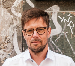
Woittennek, Michael

Woittennek, Michael

X-FAB Dresden GmbH & Co. KG

Woittennek, Michael

Abstract
Coming Soon

Biography
Michael Woittennek is CEO - Managing Director, X-FAB Dresden GmbH & Co. KG with a strong focus on cooperation and growth of the teams during the last 15 years in X-FAB. Responsibility for Dresden location including and ~580 employees in operations, facility, quality, controlling, IT and R&D. Short- and long-term goal- and priority setting responsibility. Focus on economy of scale activities (ramp 11.000 wafer starts/month) and clear support of automation roadmap to improve profitability of the site.

Fab Management Forum
X-FAB Semiconductor Foundries GmbH X-FAB Semiconductor Foundries GmbH von Podewils, Mario
Opening Remarks
von Podewils, Mario

von Podewils, Mario

X-FAB Semiconductor Foundries GmbH

von Podewils, Mario

Abstract
Coming Soon

Biography
Mario von Podewils has more than 40 years of experience in microelectronics manufacturing. In 1982, he started his career as a maintenance technician for various types of semiconductor manufacturing equipment in the microelectronics industry in Erfurt, Germany. After obtaining his degree in electronics engineering, he spent several years as a team leader responsible for equipment maintenance in various process areas in wafer fabrication at Thesys GmbH, Erfurt. From 1992 to 2001, he was project manager of national and international joint projects in the semiconductor industry, mainly funded by the BMBF or the EU.In 2001, he obtained his diploma in industrial engineering, specialising in operations and production management. Since then, he has held various positions as department and module manager for equipment engineering and the lithography module at X-FAB Semiconductor Foundries AG, among others. In 2007, he took over the position of Fab Operations Manager at X-FAB Semiconductor Foundries GmbH in Erfurt.At the beginning of 2021, he was delegated to the MEMS site in Itzehoe of the XFAB Group as Site Manager. Since autumn 2022, as Director MEMS & Erfurt Operations, he is now responsible for both wafer fabs at the Erfurt and Itzehoe sites as well as X-FAB's global MEMS production.

Fab Management Forum