A To top
AENEAS AENEAS Rohrbach, Nadja
Building Collaborative ECS projects via the Eureka Cluster Xecs
Rohrbach, Nadja

Rohrbach, Nadja
Xecs Director
AENEAS

Rohrbach, Nadja

Abstract
The semiconductor industry and actors from the full Electronic Components and Systems value chain innovate, and evolve, by a simple creed: faster, greener, cheaper. And while it might seem complex and costly to introduce novel technologies at every step of production, it is easier and more affordable than you think to implement change and gain an immediate return on investment. Whether you need to manage fierce competition or cut innovation costs, funded international collaborations are your gateway to tackle complex technological challenges, address research opportunities , grow innovative partnerships to drive technological improvement and increase profitability.Join our funding programme representative and experts and discover how funding and international industry collaborations including other actors can help your company to adopt next-generation innovations ahead of the global competition!

Biography
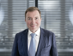
With an academic background in biology and immunology, Nadja Rohrbach spent several years as a scientific officer for a member of the German Federal Parliament. Subsequently she joined the DLR Project Management Agency, initially focusing on Eureka and network projects, before becoming head of the Eurostars group. Few years ago, Nadja was seconded by the German Federal Ministry of Education and Research to the Eureka secretariat in Brussels, where she was appointed central coordinator for the new Eureka Clusters Programme and worked with various bodies like public authorities and industry to draft the first Eureka Clusters Multi-Annual and Annual Operational Plans. One year ago, she started at AENEAS as Xecs Programme Director being in charge of the Clusters Penta and Euripides as well.

Chips Hub Europe
Agilent Technologies Agilent Technologies Brotherhood, Andrew
The Leading ICP-MS/MS Approach for Measuring Inorganic Impurities : Addressing the New Challenge of Metallic Nanoparticles
Brotherhood, Andrew

Brotherhood, Andrew
Atomic Spectroscopy Application Chemist
Agilent Technologies

Brotherhood, Andrew

Abstract
To meet the requirements for higher integrated circuit (IC) performance and improved device yield, contamination must be controlled in the wafer substrate and on the surface of the device during fabrication. Given the nanometer scale of device features, there is a critical need to monitor metallic nanoparticles (NPs), as well as dissolved metals. ​Analysis of NPs present in bulk chemicals, silicon wafers, and cleaning bath solutions is important. If a particle is present between two metal lines, it may cause electrical shorting to occur and surface defects can affect the growth of new layers on the silicon wafer. ​To fully investigate the cause/source of any particle contamination, multi-element analysis of NPs is necessary. ICP-MS is used increasingly to measure nanoparticles directly in sample solutions, using single particle inductively coupled plasma mass spectrometry (spICP-MS). With growing interest in characterizing NPs in various semiconductor samples, the technique is currently being evaluated within the industry.

Biography
Andrew Brotherhood has over 15 years’ hands-on experience with ICP-MS, ICP-OES and Ion Chromatography instrumentation. He has mainly worked in the pharmaceutical analysis industry gaining significant experience with developing and validating methods to pharma regulations. Andrew started working for Agilent in January 2018 as an Atomic Spectroscopy Application Chemist based at the Agilent Centre of Excellence in the UK.

Thursday Innovation Showcase
Airbus Airbus Ombach, Grzegorz
The Future of Air Travel Will Be Carbon Neutral and More Autonomous
Ombach, Grzegorz

Ombach, Grzegorz
Head of Disruptive R&T, Senior Vice President
Airbus

Ombach, Grzegorz

Abstract
The future of aviation is more electric and more autonomous. Reducing emissions from the transportation sector on the road, sea, and the air is one of the fastest ways to combat climate change.The aviation industry represents approximately 2.5% of global human-induced CO2 emissions. But aviation is not the problem. Emissions are the problem.Airbus, is committed to leading the decarbonisation of the aerospace sector. Airbus's vision is to reach net-zero carbon emissions by 2050. This includes reducing the CO2 emissions of our aircraft, helicopters, satellites and launch vehicles, as well as our industrial environmental footprint at sites worldwide and throughout our supply chain.Today, a zero-emission flight is closer to reality than ever. At Airbus, we are committed to developing, building and testing alternative-propulsion systems – powered by electric, hydrogen and other technologies to enable the aviation industry to disruptively reduce the CO2 emissions of commercial aircraft, helicopters, and future urban air mobility vehicles. We are working to deliver on our ambition to bring the world’s first zero-emission commercial aircraft to market by 2035.Additionally, the more autonomous flight can deliver increased fuel savings, reduce airlines' operating costs, and support pilots in their strategic decision-making and mission management. The various technology bricks help to build certifiable, safe and secure autonomy systems and programmes to power the next generation of commercial aircraft applications.

Biography
Dr Grzegorz (Greg) Ombach,Head of Disruptive R&T, Senior Vice President at AirbusGrzegorz (Greg) is passionate about managing technological innovation from an idea to broad market adoption. His combination of technology, leadership and commercial expertise together with a truly global outlook, having worked across Europe, the USA and China, puts him in a solid position to drive international market success for high-tech innovations.As a Head of Disruptive R&T, he shapes Airbus's ability to be the global leader in innovation and future technologies across all Airbus divisions. He works very closely with all businesses and divisions globally. Before as Executive Vice President, Head of Battery Systems Business and Group Strategy and Innovation at Dräxlmaier, he was responsible for the strategy for the business and led the entire product commercialisation, from the initial concept to high volume production of cutting-edge technology in a premium market for the automotive sector. One example is the first high volume production of an 800V battery system for the Porsche Taycan. Earlier, he worked at Qualcomm as a Global Vice President and General Manager of a breakthrough automotive technology licensing business.He also has experience from Siemens VDO, Continental and Brose.Grzegorz holds a PhD in Electrical Engineering from the Silesian University of Technology, Poland and a Certificate in Global Management from INSEAD, The Business School for the World. He has also been awarded Guest Professorship at the Zhejiang University in China.

Executive Forum
Alemnis AG Alemnis AG Widmer, Remo
Recent innovations in Scanning electron microscope in situ mechanical testing for semiconductor failure analysis
Widmer, Remo

Widmer, Remo
Application Engineer
Alemnis AG

Widmer, Remo

Abstract
With the growing complexity of integrated circuits (IC) comes the issue of quality control during the manufacturing process. In order to avoid late realization of design flaws which could be very expensive, the characterization of the mechanical properties of semiconductor components needs to be carried out in an efficient and standardized manner. The effects of changes in the manufacturing process and materials used on the functioning and reliability of the final device also need to be addressed.Micromechanical tests performed in situ (usually in SEM) are already being used to investigate material properties at very small scales. This talk will introduce the concept and how such techniques can specifically be applied to semiconductor materials and electronics components. Such measurements have moved beyond the basic measurement of hardness and elastic modulus to encompass a host of different mechanical properties such as strain rate sensitivity, stress relaxation, creep, scratch resistance, coating adhesion and fracture toughness by taking advantage of focused ion beam milled geometries. New developments, such as high cycle fatigue, are extending the range of properties which can be studied. Novel piezo-based nanoindentation methods are now allowing access to extremely high strain rates (>104 s-1) and high oscillation frequencies (up to 10 kHz).This talk will focus on recent developments in instrumentation for in-situ semiconductor testing at the micro and nanoscales, with specific focus on a testing platform capable of strain rate testing over the range 0.0001 s-1 up to 10’000 s-1 (8 orders of magnitude) with simultaneous high-speed actuation and sensing capabilities. Recent advances in wafer and device level automated testing, including fast mapping, will also be covered.The additional challenge of performing mechanical testing at true in-service operating conditions (e.g., over the temperature range -150 to 1000 °C) will be discussed together with the associated technological and protocol advances required. The inherent advantages of using small volumes of sample material, e.g., small ion beam milled pillars, will be discussed together with the associated instrumentation, technique development, data analysis methodology and experimental protocols. Some examples of test data will be presented on bonding pads, solder bumps and semiconductor coatings.

Biography
Remo N. Widmer holds a B.Sc and M.Sc in Earth Sciences from University of Bern (CH) and a Ph.D. in Material Sciences from University of Cambridge (UK). During the following three years of postdoc in the laboratory for micromechanics at Empa (CH) under Prof. Johann Michler, he mainly worked on extreme micromechanics of amorphous materials. He subsequently joined Alemnis AG, where he now develops novel applications for micromechanical testing.

Innovation Showcase
Alphawave IP Chan Carusone, Tony
Feeding AI’s Demand for Data

Chan Carusone, Tony
Chief Technology Officer
Alphawave IP

Abstract
Advancements in the semiconductor industry play a major role in enabling the adoption of complex Artificial Intelligence (AI) technology. With developments in AI calling for more computing power, faster storage, and more networking resources in data centers, ensuring that data speeds do not become a bottleneck is critical to furthering the potential of AI technology. To address the need for more computational power, the semiconductor industry is shifting away from monolithic dies to architectures based on chiplets. Co-packaged AI chiplet clusters can offer greater performance, but require high-speed dense interconnections and must be fed orders of magnitude more data. Unfortunately, existing connectivity technologies are simply unable to meet this demand, causing bottlenecks that limit progress on AI. Solving this bottleneck will require the semiconductor industry and interface connectivity innovators to come together, providing faster communication between AI chiplets and to external storage. Connectivity IP companies will leverage advances in semiconductor manufacturing and packaging to create interface connectivity technology that transfers data at higher rates and more reliably. The result will be massively parallel processors spread across dozens of chiplets interconnected seamlessly with terabytes per second of memory bandwidth. These innovations are necessary for chiplets to realize their fullest potential. With increasing demand for sustainable, efficient AI, the semiconductor industry and interface connectivity must work closely now to lay the foundations for the future of computing.

Biography
Tony Chan Carusone was appointed Chief Technology Officer in January 2022. Tony has been a professor of Electrical and Computer Engineering at the University of Toronto since 2001. He has well over 100 publications, including 8 award-winning best papers, focused on integrated circuits for digital communication. Tony has served as a Distinguished Lecturer for the IEEE Solid-State Circuits Society and on the Technical Program Committees of world's leading circuits conferences. He co-authored the classic textbooks “Analog Integrated Circuit Design” and “Microelectronic Circuits” and he is a Fellow of the IEEE. Tony has also been a consultant to the semiconductor industry for over 20 years, working with both startups and some of the largest technology companies in the world.Tony holds a B.A.Sc. in Engineering Science and a Ph.D. in Electrical Engineering from the University of Toronto.

Thursday Innovation Showcase
Amkor Technology Europe Portugal (ATEP) Amkor Technology Europe Portugal (ATEP) Silva, José
Amkor Activities in Portugal and Overall Trends in Europe
Silva, José

Silva, José
Vice President of Operations & R&D
Amkor Technology Europe Portugal (ATEP)

Silva, José

Abstract
Coming soon

Biography
José joined Amkor in July 2017 as part of the Nanium acquisition and is currently Vice President of Operations & R&D at ATEP. He started his career in the semiconductor industry at Siemens and later held management positions as Quality Director and Operations Director at Infineon, Qimonda and Nanium. José holds a degree in Electrical Engineering from Universidade do Porto and an MBA from Porto Business School.

Advanced Packaging Conference
AMO GmbH AMO GmbH Rinke, Gordon
The European 2D-Experimental Pilot Line as a Platform for Novel Sensor Concepts
Rinke, Gordon

Rinke, Gordon
Vice Head of Graphene Electronics Group
AMO GmbH

Rinke, Gordon

Abstract
Devices based on 2D materials like graphene have attracted a lot of attention due to its extraordinary electronic, optical, and sensing properties and consequently its effect on the device performance. However, the fabrication on large scale and thus the availability as well as the introduction into the market remains challenging. With the mission to efficiently close the gap between university research and industrial application, the European project 2D Experimental Pilot Line (2D-EPL) tries to establish a route for 2D material integration on large scale by developing critical tools and materials and make 2D materials compatible to the standards in industry. In this framework AMO provides as one of the partners multi project wafer (MPW) runs, with the aim to integrate 2D materials on large scale and to give access to this technology for interested customer. In this talk, I will give an insight to the facilities at AMO, the 2D-EPL project and some application examples of our research on sensors and detectors based on 2D materials.

Biography
Dr. Gordon Rinke obtained his PhD in Materials Science from the EPFL Lausanne, Switzerland in 2013. After spending over 6 years in industry for a semiconductor tool manufacturer as lead process engineer, he joined AMO GmbH in Aachen, Germany in 2021 as Project Manager for the European 2D Experimental Pilot Line Project and became deputy of the graphene electronics group. His background covers the nanostructure growth and fabrication of organic and inorganic materials as well as process development and optimization.

Materials Innovation
ams-OSRAM AG ams-OSRAM AG Milnikel, Jens
Semiconductor Companies Shaping the Transformation of the Healthcare Industry with Optical Solutions
Milnikel, Jens

Milnikel, Jens
EVP & GM BU Image Sensor Solutions
ams-OSRAM AG

Milnikel, Jens

Abstract
The medical industry is undergoing a transformation that will impact the way people care about their personal health. In a social environment of an aging but tech savvy population, with birth rates at a minimum in decades, it becomes increasingly important to redefine the way we understand personal health.Emerging technologies and sensors play a key role to bring diagnosis and treatment out of the traditional channels, enabling personalized, participative and predictive medicine in an agile and cost efficient health system.Jens Milnikel will explain his vision on a new era of personal healthcare and how ams-OSRAM sees precision medicine as one of the core pillars of their future strategy, and can shape it with solutions like vital signs monitoring, ultra-accurate temperature measurements, UVC or Bluetooth connected LTF tests amongst others.

Biography
Jens Milnikel can look back on more than 20 years’ experience in the semiconductor industry. After several years at Roland Berger Strategy Consulting, he joined Infineon Technologies in 2001, holding several management positions.With the photovoltaic industry on the rise, he moved to an international building material conglomerate. As managing director, Jens established and expanded the global solar business within this company. In 2013 Jens joined Philips Lighting, where he shaped the system and service business as well as the transition from conventional to LED lighting.Jens took on his current position as SVP at ams OSRAM in 2019, growing the Business Line Illumination. Since May 2022 he has been managing the Business Unit ISS and is also part of the ams OSRAM corporate managing team.Jens has a degree in Industrial Engineering from the Karlsruhe Technical University.

Smart MedTech
Applied Materials Applied Materials Neuber, Andreas
Sustainability Improvements in Semiconductor Manufacturing Using Smart Manufacturing Technologies
Neuber, Andreas

Neuber, Andreas
Director Environmental Services
Applied Materials

Neuber, Andreas

Abstract
Coming Soon

Biography
Andreas Neuber, Ph.D. has been a Senior Director at Applied Materials since 2008. He has published 80+ papers related to semiconductor fab and facility design, sustainable design and energy savings, water management and recycling, contamination control, and industrial engineering.Prior to joining Applied Materials, Andreas Neuber was Vice President for M+W Zander. During his 18 years at M+W Zander, was involved in semiconductor fab construction and operation/optimization in many locations.Andreas Neuber received a PhD degree in Chemical Engineering from University of Technology Dresden. He is co-chair of the SEMI ESEC task force and the IRDS EHS/S Energy and water reduction roadmap.

Smart and Green Manufacturing Summit
Applied Materials Applied Materials Chudzi, Michael
A Materials to Systems Understanding of a BEOL Embedded Analog NVM Memory Technology for Edge Compute Applications
Chudzi, Michael

Chudzi, Michael
VP of Technology for IMS
Applied Materials

Chudzi, Michael

Abstract
Coming Soon

Biography
Dr. Chudzik is VP of Technology for IMS at Applied Materials focusing on device and module engineering solutions in the specialty and packaging segments.He has a PH.D in Electrical engineering from Northwestern University. Mike has been at Applied Materials for 8 years and prior to that he worked at IBM for 14 years in various roles in DRAM and CMOS process integration and management.

Future of Computing
ASE Europe ASE Europe Factor, Bradford
Packaging for Integrated Photonics
Factor, Bradford

Factor, Bradford
Director, Packaging Technology
ASE Europe

Factor, Bradford

Abstract
Coming Soon

Biography
Bradford Factor received his Ph.D. from Stanford University in Applied Physics in 1991 and worked in research in France and Greece, and at the Polymers Division of NIST in Maryland, USA. Bradford began his career in the semiconductor packaging the mid 1990’s, first at Intel and then at Lucent Microelectronics in BGA and flip chip materials and assembly. He subsequently worked on packaging of planar waveguide circuits and optoelectronic devices at Corning in France. Since joining ASE Europe in 2002, he supports the European customer base focusing on advanced technologies, including flip chip, wafer level and fan-out packaging, system-in-package as well as power packaging. He is a currently a board member of the IEEE EPS chapter in France, and has received several patents and published several journal articles.

Integrated Photonics
ASE, Inc. ASE, Inc. Chang, Yin
Advanced Packaging: Enabling a New Generation of Silicon Systems
Chang, Yin

Chang, Yin
Sr. Vice President, Sales & Marketing
ASE, Inc.

Chang, Yin

Abstract
Demand for new efficiencies in the semiconductor design and manufacturing process is propelling the crucial role of packaging to deliver on requirements related to miniaturization, power, and performance. During his keynote presentation, Yin Chang will explore heterogeneous integration and chiplet innovation, and describe how advanced packaging technologies are enabling highly complex system integration. With applications such as automotive and power management demanding significant attention, he will highlight solutions that are helping create a smarter and more sustainable world for generations to come.

Biography
Ingu Yin Chang is Senior Vice President, Sales & Marketing, at ASE, based in Sunnyvale, California. In his current role, he is responsible for developing and executing sales strategy, while driving marketing activities for ASE’s expanding packaging, systems, and integration solutions portfolio.Prior to joining ASE in 2013, Yin was CEO of Vertical Circuits Inc. (VCI), a company focused on the development of next generation vertical interconnect for next generation silicon integration. Previously, Yin performed a variety of management roles covering sales and operations at Amkor with responsibility for the Greater China region. He has over twenty years of leadership experience in executive management, sales, business development, IP management and strategic alliance.Yin received his material science engineering degree from University of California, Berkeley.

Advanced Packaging Conference
ASM International ASM International Sprey, Hessel
Opening Remarks
Sprey, Hessel

Sprey, Hessel
Manager External R&D and Cooperative Programs
ASM International

Sprey, Hessel

Abstract
Coming Soon

Biography
Hessel Sprey received his M.Sc. in experimental physics from the University of Leiden (The Netherlands) in 1989, and joined ASM International in 1990.He has been active in equipment and process R&D at various ASM and customer locations for several of ASM’s product lines, since 1996 in project and team leader positions.He has been project and workpackage leader for several European projects, is (co-)author of more than 60 scientific papers and conference contributions on deposition processes, equipment and applications, and holds 22 patents and patent applications.He is currently based in Leuven, Belgium, with as main activity the coordination of ASM's External R&D activities and cooperative programs.

Materials Innovation
ASM International ASM International Givens, Michael
How Atomic Layer Deposition Impacts the Logic & Memory Industries
Givens, Michael
Senior Director & Executive Technologist
ASM International

Givens, Michael

Abstract
As the scaling of device densities continues to follow Moore’s law, the semiconductor industry has adopted increasingly more complex materials, architectures and 3D geometries while simultaneously driving down most of the critical dimensions into the nanoscale range. In this talk, we will review the evolution of device scaling in Logic and Memory and outline how future architectures will impact material and processing requirements. We will first present an overview of how Atomic Layer Deposition (ALD) technologies have driven the industry forward through multiple material and architectural inflections over the past 15 years, such as adoption of FinFET and Gate-all-around (GAA) for Logic and 3D-NAND for Memory. Future integration schemes such as Complementary FET (CFET) and 3D-DRAM and novel emerging materials will also be discussed in the context of the opportunities and challenges that ALD will help to address.

Biography
Dr. Michael Givens, Ph.D. is Senior Director & Executive Technologist with ASM's Corporate R&D organization. He is currently based in Leuven, Belgium where he directs programs focused on the development of ALD and Epi chemistries, processes, and novel materials for Emerging Logic and Memory device technologies. He has over 30 years' experience in the industry, over 20 of that with ASM, holding various roles in materials, process, device, and equipment development from Pathfinding through HVM phases. He received his BS, MS, and PhD degrees in Electrical Engineering from the University of Illinois at Urbana-Champaign.

Materials Innovation
ASML ASML Hajiahmadi, Reza
Wafer contamination detection: an unsupervised learning approach
Hajiahmadi, Reza

Hajiahmadi, Reza
Data scientist
ASML

Hajiahmadi, Reza

Abstract
The wafer particle contamination (backside and frontside) inside semiconductors factories is often very late detected in the production process and the impact of that is significant, as it can introduce yield loss and large down time on the litho tools.Unfortunately, there is no easy-to-use monitoring tool to detect, quantify and classify all forms of particle contamination on the wafer. We have developed a solution based on the open-source data science KNIME Analytics platform, in which we have used signal processing and machine learning techniques to detect, quantify and classify the contaminated areas using wafer height data. To be more specific, our solution is able to fully detect backside particles clamped between the wafer and the wafer table burls. And as for the frontside particle, our tool is able to detect the ones that are larger than 10nm in height and 3.3 um in area.The prototype we developed contains a dashboard deployed in a web browser on the lithography tools and can easily be used real-time by customers in their fabs. The users can easily monitor wafer contamination and the health of the wafer table instantly and through time without the need to store large amount of data and/or installing tools on local computers.The proposed solution is able to automatically detect any number of clusters of bad spots in a wafer map. The solution consists of wafer’s height data units, spot detection, spot classification and KPI reporting and visualization. In more detail:Slope detection mechanism of bad spots instead of plain wafer observation and a new fully automated algorithm (DBSCAN, a density based algorithm that does not need prior training nor the number of groups/clusters that they data contains) to classify the detected spots. The classified spots/shapes help the operator find the root causes of the contamination.Reporting (in the form of an inline monitoring dashboard deployed on the litho tool) the statistics and the characteristics (shape, hint on root cause, etc.) of the identified clusters of contamination particles to the users and notifying the operator if the level of contamination exceeds a defined threshold.Identification of persistent spots (wafer heatmap) on multiple wafers that could provide insight on whether the contamination is caused by wafer table damage, backside features and/or other process related issues in the fab.­­

Biography
Reza Hajiahmadi obtained his PhD, cum laude, in Applied Mathematics from Delft University of Technology in 2015. He has been working at ASML as a data scientist and senior lithography engineer for 6 years and has published several patents and publications as part of his research in metrology, lithography and field data mining techniques.

Innovation Showcase
Athinia Athinia Matz, Laura
How the Semiconductor Industry Can Leverage Data Expertise From Healthcare
Matz, Laura

Matz, Laura
Chief Science and Technology Officer, Merck and CEO
Athinia

Matz, Laura

Abstract
The semiconductor industry is experiencing a time of unprecedented disruption. Lately, we are witnessing multiple investments and a growing importance in regions around the world to pass legislation to reinvigorate local semiconductor infrastructures and supply chains. As the Chief Science and Technology Officer of Merck, a company active in the areas of Healthcare, Life Sciences, and Electronics, Dr. Laura Matz will bring a new perspective highlighting the importance of looking at and learning from data-driven innovations in other industries, specifically Healthcare.The immense amounts of data produced today creates opportunities for not just a single company but for the entire value chain to achieve excellence in production, innovation, and cost reduction. Deep-diving on Syntropy´s learnings within Healthcare, Dr. Laura Matz will outline the path for the semiconductor ecosystem to adopt industry-wide data collaboration to speed up innovation. She will also highlight how Athinia™ addresses this challenge, with a strong focus on data security and intellectual property protection.

Biography
Dr. Laura Matz is the Chief Science and Technology Officer for Merck, driving innovation and digitalization in Merck across the 3 business sectors, Life Sciences, Healthcare and Electronics. Serving as an Executive Vice President within Merck, her areas of responsibility include Digital, Enterprise Data, Future Insight, as well as the company’s global innovation hubs in China, Israel, the U.S., and at its Darmstadt HQ. In addition, Laura is CEO of the newly launched data sharing platform company, Athinia™, which is focused on enabling secure data sharing within the semiconductor ecosystem. Laura joined Merck in 2019 through the acquisition of Versum Materials.She possesses 20 years of experience in semiconductor manufacturing, and a decade of experience in running semiconductor materials businesses. Prior to moving to the CSTO role, she served as the Head of Planarization in the semiconductor materials business, while also heading a sector-wide digital program for quality innovation with the company’s electronics customers. Laura started at Versum Materials in 2016, having previously worked at Air Products and Texas Instruments.Laura is a strong advocate for young talent in science and engineering. She has collaborated with ASU over the past 5 years to build a strong pipeline of interns. In 2020, Laura joined the AICHE (American Institute of Chemical Engineers), ILI board (Institute for Learning and Innovation), which serves as a conduit for advancing chemical engineering talent for the U.S. Given that artificial intelligence and machine learning are enablers for the continued growth in the semiconductor industry, she is a member of the SEMI Smart Manufacturing board, as well as the local AZ SEMI board.Laura has a Ph.D. in Analytical Chemistry from Washington State University, and an undergraduate degree from the Indiana University of Pennsylvania.

Executive Forum
Atotech Atotech Schmidt, Ralf
Optimization of the Cu Microstructure to Improve Cu-to-Cu Direct Bonding for 3D Integration

Schmidt, Ralf
R&D Manager Semiconductor
Atotech

Schmidt, Ralf

Abstract
Advanced packaging solutions and heterogeneous integration are key technologies to enable devices with improved operating characteristics, including higher performance, increasing power efficiency, and decreasing form factor. Packages with high I/O densities are required to efficiently combine, e.g., processing and memory units but impose restrictions to the pitch of the interconnects. Conventional technologies, including wire bonds and flip chip bonds are limited to larger pitches and, therefore, not suitable to meet the requirements of upcoming packaging technologies with respect to I/O densities. Direct copper-to-copper interconnects are supposed to allow such small pitches of 10 µm or even below. However, formation of such bonds usually requires high temperatures and pressures. Temperature-sensitive devices like DRAM components restrict the maximum temperature that can be applied to the package. Thus, copper material is required, which allows bond formation at relatively low temperatures. In this context, hybrid bonding processes were discussed that involve initial bond formation via the usually oxide-based dielectric at room temperature followed by copper-to-copper bonding at elevated temperatures. The copper material is usually prepared by electrolytic deposition and the properties of the respective deposits may be modified by properly designed organic additives as well as process parameters. Strong bond formation of the copper should be obtained upon grain growth over the interface of the two deposits, which are brought into contact during the bonding step. In order to facilitate such growth at relatively low temperatures, suitable microstructures need to be prepared. Ideally, morphologies should be chosen in a way that they can be maintained throughout all process steps after the electrolytic deposition but, at the same time, allow grain growth over the interface during copper-to-copper bonding. Various strategies to enable improved seamless grain growth and maintain suitable microstructures throughout the preceding process steps will be compared in terms of the resulting copper microstructures after bonding. In this context, different electrolytic copper deposition processes, the resulting morphologies, as well as their respective advantages and challenges with regards to copper-to-copper bond formation will be discussed.

Biography
Experience with process development for semiconductor applications since 2016Author of numerous scientific publications and patents in the area of metallization for semiconductor applications.Lecturer at the Humboldt University of Berlin since 2013Experience with metallization processes for electronics industry for > 10 years

Advanced Packaging Conference
ATREG, Inc. ATREG, Inc. Rothrock, Stephen
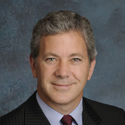
Overview Of The Global Semiconductor Manufacturing Asset Market
Rothrock, Stephen

Rothrock, Stephen
Founder, President & CEO
ATREG, Inc.

Rothrock, Stephen

Abstract
Coming Soon

Biography
Stephen founded ATREG [ www.atreg.com] in 2000 to help global advanced technology companies divest and acquire infrastructure-rich manufacturing assets, including wafer fabs (front- and back-end) as well as MEMS, solar, display, and R&D facilities. Over the last 20 years, his firm has completed 40% of all global operational wafer fab sales in the semiconductor industry, a total of 100 transactions representing a value of over $5 billion. Recent global acquisitions and dispositions have involved Allegro MicroSystems, Fujitsu, GF, IBM, Infineon, Matsushita (Panasonic), Maxim, Micron, NXP, onsemi, Sony, Qualcomm, Renesas, Texas Instruments, and VIS to name just a few.Prior to founding ATREG, Stephen established Colliers International’s Global Corporate Services initiative and headed the company’s U.S. division based in Seattle, Wash. Before that, he worked as director for Savills International commercial real estate brokerage in London, UK, also serving on the UK-listed property company’s international board. He also spent four years near Paris, France working for an international NGO. Stephen holds an MA degree in Political Theology from the University of Hull, UK and a BA degree in Business Commerce from the University of Washington in Seattle, USA.

ATREG PANEL
B To top
Bethtel Corporation Bethtel Corporation Moharram, Abdelkarim
Panelist
Moharram, Abdelkarim

Moharram, Abdelkarim
Manager, Business Development, Semiconductors, Manufacturing & Technology
Bethtel Corporation

Moharram, Abdelkarim

Abstract
Coming Soon

Biography
Abdelkarim’s experience is derived from the planning, development, and delivery of megaprojects in the energy, chemical, marine, infrastructure, nuclear, and manufacturing sectors. He is currently focused on growing the portfolio of capital projects for Bechtel’s Manufacturing & Technology business. He initially joined Bechtel’s corporate venture capital group focused on evaluating and investing in technologies with the purpose of designing and building multi-billion assets faster, safer, and more sustainably.Abdelkarim holds a BSE from Duke University. Through an appointment by the Governor of Virginia, he serves on the Board of Trustees of GENEDGE (part of the National Institute of Standards & Technologies) as well as an advisory committee member for the congress-supported Virginia Manufacturers for Strategic Industries.

ATREG PANEL
brainjo GmbH brainjo GmbH Gnerlich, Christian Michael
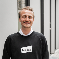
AR/VR - Metaverse :Virtual Reality for Mental & Physical health in B2B
Gnerlich, Christian Michael

Gnerlich, Christian Michael
CEO
brainjo GmbH

Gnerlich, Christian Michael

Abstract
AR/VR | Metaverse | Virtual Reality for mental & physical health in B2B | Brain Computer Interfaces | silicon valley accelerator participant | Seed Stage Startup

Biography
CEO | Co-FounderbrainjoJune 2018-Today - 4 years 5 monthsSoftware engineer (project related)Coleida Ltd.Feb. 2019-May 2019 - 4 monthsManager brainboost AmbergBrainboostOct. 2017-Nov. 2018 - 1 year 2 monthsCo-Founder in the Exist funded startup Herzheim.Federal Ministry for Economic Affairs and Energy2017-July 2017 - 7 months Jan.FounderOut of the Box Foundation (for ADHD).2016-2017 - 1 year2016-2017 - 1 yearStudent Assistant | Institute for Sustainability in Technology and EconomicsS.OTH Amberg-WeidenOTHMarch 2016-Sept. 2016 - 7 monthsInitiator | Students for Refugees Amberg-WeidenOTH Amberg-WeidenJan. 2015-2016 - 1 year 1 monthAwardsBCI Hackathon IEEE Brain BR41N.IO Prize 2020From: g.tec neurotechnology Austria - Jan. 2020Hackathon Regensburg (Winner)From: Hackaburg Regensburg - Jan. 2019Competition: hospital of the future (winnerFrom: Medical Valley - Jan. 2017Award for ethics and sustainabilityFrom: East Bavarian Technical University Amberg-Weiden - Jan. 2016

Fab Management Forum
C To top
C12 C12 Desjardins, Pierre
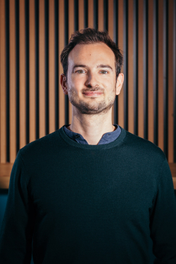
Building Scalable and Ultra-Coherent Quantum Computers with Carbon Nanotubes
Desjardins, Pierre

Desjardins, Pierre
CEO & co-founder
C12

Desjardins, Pierre

Abstract
C12 builds next generation quantum computers powered by the most elementary material: carbon nanotubes. Unlike other quantum computers, we use carbon nanotubes as the fundamental building block of our processor. By combining the power of an ultra-pure material with an easy-to-manufacture semiconductor device, we are building the next generation of quantum computers, designed to provide unparalleled fidelity, connectivity, and scalability. Our first product will be a quantum accelerator able to run hybrid quantum-classical algorithms for chemistry applications.

Biography
Pierre Desjardins holds a Master of Science degree from Columbia University (2013) and later worked for six years as a strategy consultant. He founded the startup C12 in 2020. C12 is leading the next materials leap in quantum computing and is on a mission to build reliable quantum computers to speed up highly complex computing tasks, thanks to a unique know-how developed at CNRS and the Physics Laboratory of the Ecole Normale Supérieure in Paris. C12 believes that only a materials science breakthrough will enable large-scale quantum computers.

Future of Computing
Carl Zeiss Digital Innovation GmbH Carl Zeiss Digital Innovation GmbH Hörr, Christian
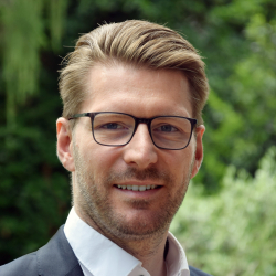
The Pareto Principle in Industry 4.0

Hörr, Christian

Hörr, Christian

Carl Zeiss Digital Innovation GmbH

Hörr, Christian

Abstract
More than ten years after the term has been coined, the idea of Industry 4.0 is finally about to lose its mysteries. Although its disruptive potential is widely accepted nowadays, the digital transformation of the shopfloors takes place much slower than originally expected. We summarize a few key learnings and typical impediments from current practice and discuss how to overcome them by applying the Pareto principle.

Biography
Dr Christian Hörr has been working as a delivery lead at ZEISS Digital Innovation since July 2021 and consolidates the development activities surrounding Industry 4.0. He uses his practical experience gained over a decade as a full-stack developer and head of development in the field of optical measurement technology, robotics and automation technology.

Fab Management Forum
CEA-Leti CEA-Leti Joly, Sylvie
Will More-than-Moore Technologies with 3D Integration meet the Challenges of Edge AI Devices ?
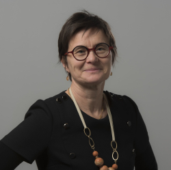
Joly, Sylvie

Joly, Sylvie
Parnerships Manager 3D integration and packaging
CEA-Leti

Joly, Sylvie

Abstract
In the world of high performance computing, over a decade the performances of the computing has constantly increase beyond the almost automatic but slowing down improvement in processor performance with Moore's Law. Big players have moved to new architectures such as chiplets only possible thanks to the integration of More-than-Moore technologies. 2.5D and 3D integration, memory cubes, accelerators and heterogeneous architectures are key elements of the success towards performance and energy efficiency. This transition has shown clear benefits and sustainability for HPC market. The question is still open for Edge AI components where real time, ultra-low power, large amount of data, low cost are the main drivers: how can 3D integration play a role for these embedded processors? CEA-Leti has been involved for more than two decades in 3D integration with industrial partners. This presentation will discuss about:- What are the main drivers for computing in edge devices ?- What could be the architectures’ new paradigm ?- How 3D integration will be an enabler, and how CEA-Leti’s roadmap supports this promising technology

Biography
Sylvie Joly is currently working as 3D integration and packaging Partnerships Manager at CEA-LETI. Sylvie received M.Sc. in Microelectronics from ISEP "Institut Supérieur d'Electronique de Paris" in 1989. She completed her education with a Master in Marketing and Innovation at the Grenoble Ecole de Management (GEM) in 2001. Prior to this position, she worked for more than 8 years as display business developer at CEA-LETI. In 2004 as Sr. Marketing Engineer in the CEA's Technology Transfer Department, she built a strong experience in setting up and managing technical marketing surveys. Before joining CEA, she spent 10 years in the industry as an R&D engineer, and 8 years as Sales engineer in several companies including Hewlett Packard and Ericsson.

Future of Computing
CEA-Leti CEA-Leti Signamarcheix, Thomas
Opening Remarks by Session Chair
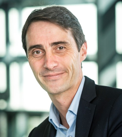
Signamarcheix, Thomas

Signamarcheix, Thomas
Vice President, Strategic Development,
CEA-Leti

Signamarcheix, Thomas

Abstract
Not Applicable

Biography
Thomas Signamarcheix joined CEA-Leti in 2008, and in 2011, he was named manager of a research laboratory on substrates engineering. From 2015 to 2019, he was in charge of business development management for Leti's Silicon Component Division and Architecture and Embedded Software Division.As Key Account Manager of several strategic collaborations, he also directly managed a wide range of activities (semiconductor, alternative energy, sensor, radio-frequency, etc.) promoting innovation at both hardware and architecture levels. He has been vice president of CEA-Leti's strategic development since 2020, managing Leti's strategic program (Quantum Electronic, Artificial Intelligence, wearable healthcare devices and mixed reality) and strategic partnerships. He has a PhD in the physics of semiconductor devices from Grenoble Institute of Technology (INPG), and he has contributed to nearly 10 patents and co-authored more than 50 scientific publications.

Future of Computing
CEA – LETI CEA – LETI Kerdilès, Sébastien
Exotic applications of nanosecond laser annealing
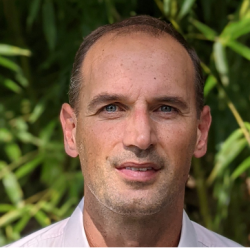
Kerdilès, Sébastien

Kerdilès, Sébastien
Head of Thermal Treatments Engineering
CEA – LETI

Kerdilès, Sébastien

Abstract
The need for lower and lower thermal budget in microelectronics has driven annealing technologies from furnaces to millisecond processes. The era of nanosecond laser annealing (NLA) is coming. On one hand, such technique enables treatments at very high temperatures in the melt and sub-melt regimes, with unprecedented cooling rates, that give access to very high active dopant concentrations. One the other hand, thanks to its short pulse duration, NLA also enables surface heating with an excellent in-depth selectivity, which is particularly suited for various 3D architectures. In this presentation, several More-than-Moore applications of NLA currently developed at CEA-LETI will be shared. The use of NLA will be illustrated for 3D sequential integration, for ferroelectric memories integrated in the BEOL and for exotic applications leveraging superconducting silicon.

Biography
Dr. Sébastien Kerdilès received a Ph.D. degree in materials science from the University of Caen, France, in 2000. Then, he worked for 2 years for a start-up in the Paris area. From 2002 to 2013, he worked for SOITEC as a research staff member first, then as a technology development manager, and finally as an SOI designer. During this period, he contributed to the industrialization of 200 & 300mm SOI substrates manufacturing, including RF-SOI and Fully depleted SOI. In 2013, he joined CEA-LETI, where he is in charge of thermal treatments. His research interests include the investigation of pulsed laser annealing for various applications such as 3D integration, memories, and MEMS. He authored or co-authored more than 50 journal articles and conference papers and holds over 20 patents.

SCREEN
CEA, Leti MINATEC CEA, Leti MINATEC Sousa, Veronique
Overview of the normally-OFF GaN-on-Si MOSc HEMT transistor in the fully recessed gate architecture
Sousa, Veronique

Sousa, Veronique
Head of Laboratory for Power Semiconductor Devices
CEA, Leti MINATEC

Sousa, Veronique

Abstract
Gallium nitride power switches have emerged in industry to provide solutions for a wide range of power applications. Different approaches are considered to obtain a normally-off operation of the GaN transistor. While the pGaN gate architecture is more mature and already commercially available, the recessed gate technology including an insulated gate potentially offers better performance. In this presentation, we will detail the latest integration process developed at Leti to fabricate fully recessed gate MOSc-HEMT transistors. We will present the electrical characteristics of the devices, evaluated both at the wafer level and on packaged devices. We will thus highlight the advantages of this recessed-gate technology with respect to the pGaN gate technology, in particular the lower temperature coefficient of the resistance of the device, or the reduced gate current, or the shorter switching time.

Biography
Véronique Sousa graduated in 1994 from the University of Grenoble Alpes in the field of Materials Science and Engineering. She joined the CEA-Leti-MINATEC-Campus in 1998. For twenty years, she conducted R&D projects dedicated to the optimization of various resistive memory technologies, including phase change memories. Since 2018, the focus of her work has shifted to solid-state power devices. In 2020, she took over as head of the CEA-Leti Power Semiconductor Devices Laboratory.

Electrification & Power Semiconductors
centrotherm Clean Solutions centrotherm Clean Solutions Stover, Adam
Effect of Gas Abatement Selection and Destruction Efficiency on Carbon Neutrality Goals

Stover, Adam

Stover, Adam
Chief Technology Officer
centrotherm Clean Solutions

Stover, Adam

Abstract
Process gas abatement is the backbone of any fab's environmental stewardship program. Proper abatement minimizes not only toxic and hazardous gas release to the environment, but also particulate matter and waste water. Increasingly, gas abatement is measured against its carbon footprint for the input power source, be it electrical or fuel. There is currently a push to go for "carbon free" abatement, using either hydrogen as the fuel gas or electrical systems powered by renewable energy. This goal is indeed laudable, however any carbon footprint calculation should also include the input fuel gas destruction, as they can have extremely high global warming potentials, far above and beyond the input electricity or methane.To that end, this paper makes a full comparison of the carbon footprint for various abatement technologies, taking into account various process gas destruction efficiencies to determine if the power carbon footprint outweighs the non-abated process gases. Additional analyses for regional power generation carbon footprint are also performed.

Biography
Dr. Stover is currently the Chief Technology Officer for centrotherm Clean Solutions USA, based in Albany NY. After completing his bachelors degree in chemistry from Haverford College and PhD from The Johns Hopkins University, he has spent the last 8 years in the semiconductor industry, focused on abatement and achieving sustainability goals.

Smart and Green Manufacturing Summit
Cimetrix Incorporated Weber, Alan
The Role of Streaming Data in Smart Manufacturing: Methods, Applications, and Benefits
Weber, Alan

Weber, Alan
VP, New Product Innovations
Cimetrix Incorporated

Abstract
With semiconductor factories worldwide running a full capacity in most market segments and facing new supply chain challenges every day, it is no wonder that productivity is now an important careabout across the industry. Factory managers carefully monitor their Key Performance Indices (KPIs) for any indications of lost productivity so they can react quickly to identify and address the root causes of these excursions.It is no longer sufficient to know precisely how well you did last week or even yesterday. Rather, it is important to have a fairly good idea of how well your factory is running right now. This means optimizing the tradeoffs between quality, throughput, capital effectiveness, delivery performance, and perhaps other metrics on a continuous basis.In such highly constrained situations, the value of the “right” answer decreases rapidly over time, which is the principal criterion for using streaming data in the manufacturing applications that most affect these KPIs. Since the data sources that most accurately represent the true status of manufacturing operations at any instant are the units of manufacturing equipment in the factory, it follows that an equipment integration platform capable of high-volume streaming data collection is a vital component in the factory system infrastructure. This presentation describes such an environment and highlights not only the sources and methods for streaming equipment data, but also some of the key applications and their stakeholders that leverage this capability. It also identifies the industry standards that are already in place for calculating a wide range of productivity metrics that can impact supply chain performance.

Biography
Alan Weber is currently the Vice President, New Product Innovations for Cimetrix Incorporated. Previously he served on the Board of Directors for eight years before joining the company as a full-time employee in 2011.Alan has been a part of the semiconductor and manufacturing automation industries for over 40 years. His expertise includes semiconductor design automation, equipment and factory control system architectures, Advanced Process Control (APC) and other key manufacturing applications, SEMI Information and Control standards (especially GEM300 and EDA/Interface A), and Smart Manufacturing Technology.Alan holds Bachelor’s and Master’s degrees in Electrical Engineering from Rice University.

Thursday Innovation Showcase
CITC CITC Smits, Edsger
Reliability Characterization of Silver Sintering for Die Attach Applications
Smits, Edsger

Smits, Edsger
Program Manager
CITC

Smits, Edsger

Abstract
With advances in miniaturization of electronic components, there is a trend towards ever increasing power density in semiconductor devices. In part, Wide-Band Gap (WBG) materials such gallium nitride (GaN) and silicon carbide (SiC) have enabled more efficient devices but also allowed for much higher operating temperatures. Consequently power dissipation and mechanical stresses in electronic packages have increased dramatically. From environmental perspectives, there is a strong drive to phase out lead-based solder.Discrete components are commonly assembled in packages based copper lead frames. The key challenge for such packages are the mismatches in coefficient of thermal expansion (CTE) between Cu lead frame and WBG power dies. During operation, the packages repeatedly undergo temperature swings, causing repeated thermomechanical stresses and fatigue. When not mitigated, these stresses lead to premature failure of the electronic components.Silver Sinter pastes (pressure based and pressureless) are a promising replacement of lead rich solder combining superior thermal and electrical performances. It is the scope of major research activity but a reliable solution for attaching WBG semiconductors to copper bases while retaining superior thermal and electrical performances has proven to be challenging. Unlocking the full potential of WBG semiconductor power electronics will hinge on solving these technological challenges at the package level.In this presentation, the author presents an overview of CITC research activities on advanced packaging with a focus on packaging for power electronics and silver sintering solutions. An overview of the current state of silver sinter materials is provided. The performance and limitations of the materials are addressed. Beyond materials, methods used to investigate the performances and degradation will be covered as well as the thermomechanical simulations for predicting package reliability.

Biography
Edsger Smits received his Ph.D. with honors from the University of Groningen in the field of organic electronics. In 2009, he joined TNO/Holst Centre focusing oxide based thin film transistors for displays, flexible and stretchable sensors and electronics for bio-medical applications. In 2021 he become responsible for the “Power Packaging “ at CITC. Topics of interests include mini and micro led, laser transfer, flexible and stretchable electronics and power packaging.

Advanced Packaging Conference
Cohu Cohu Wagner, Markus
The Challenges in Testing Small and Highly Integrated Devices in a Massive Parallel Test System

Wagner, Markus
Engineering Manager - Interface Solutions Group
Cohu

Wagner, Markus

Abstract
The triumph of electronic components started in the 1950s with the introduction of semiconductor transistors. Since this time the content of electronics has risen significantly. Innovations in the semiconductor industry are supporting the megatrends like mobility car electrification including ADAS-systems, sensors, connectivity, and advanced security.This trend drives demand for enhanced packaging concepts like system-in-package (SiP), SoC and heterogeneous integration, as well as optimized existing and new materials that support package miniaturization including pad size reduction, smaller pad to pad distance and thermal performance.Time to market and cost are the main challenges for new electronic technologies that will be deployed in mass production.This Presentation describes the development of a contactor for singulated, small WLCSP devices in massive parallelism test, supporting more than 200 contact sites. It considers different aspects which address the challenges of reliable and cost-efficient device testing. The active retracting technology in the contactor increases the reliability of processing the devices after test as well as supporting force-controlled device handling and methods of accurately aligning contactor probes to fine-pitch device pads or balls. It further addresses the cost-effectiveness by supporting highly parallel testing and performance monitoring over the entire lifetime to optimize maintenance intervals.by an integrated track and trace featureThe presentation will also review the thermal aspects of testing devices in a high parallelism environment.This approach requires close cooperation with the Handler supplier in order to optimize the overall performance of the entire system

Biography
Markus Wagner is Engineering Manager of the Interface Solutions Group at Cohu and is based out of Kolbermoor, Germany. Markus graduated from the University of Rosenheim with a Diploma in Mechanical Engineering. He has been in the semiconductor final test environment more than 20 years with Cohu, a provider of semiconductor equipment and services for the back-end semiconductor manufacturing. Markus has held a number of management positions in engineering and product marketing and holds several patents for innovative contacting solutions. Over the years he has gained experience in integrating contactors solutions into MEMS and final test systems.

Advanced Packaging Conference
Comet PCT Comet PCT Fasel, Marco
Panelist
Fasel, Marco

Fasel, Marco
Industrialization Team Leader
Comet PCT

Fasel, Marco

Abstract
Coming Soon

Biography
Marco, a qualified Mechanical Engineer, joined Comet PCT in 2018 as Development Engineer & Project Manager. In 2022, he was promoted to Team Leader Industrialization and now leads a team responsible for New Product Introduction and Product Support for vacuum capacitors.Marco has just completed his EMBA in General Management from the Berne University of Applied Sciences. He lives and works in Switzerland where Comet has its headquarters.

The Future of Work
Comet Yxlon Comet Yxlon Drolz, Isabella
The Future of Advanced Packaging Inspection is X-ray!
Drolz, Isabella

Drolz, Isabella
VP Product Marketing
Comet Yxlon

Drolz, Isabella

Abstract
The global demand for high-end computing power driven by smartphones, IoT applications, High-performance computing, and new mobility applications is constantly rising while facing miniaturization demands. The semiconductor industry is all about identifying and solving these challenges and thereby, yield and process control is core for foundries and its importance increased even more through the introduction of advanced packaging.In today’s environment two things can be observed. One, prototyping and verification costs exponentially increase while node sizes decrease. Two, a change from typical inspection methods like optical or FIB-SEM to advanced non-destructive inspection techniques like X-ray inspection.Ultimately advanced packaging companies seek non-destructive automated inspection tools which are fast enough to provide value within their production processes, increase yield and reduce waste at an early stage. This presentation will give an overview on how X-Ray and CT inspection can provide value-added data and information for exactly that.

Biography
Isabella Drolz is the Vice President Product Marketing at Comet Yxlon, which is the industrial X-ray & CT inspection system division of Comet. Comet Yxlon provides X-ray & CT inspection solutions for R&D labs & production environments, especially for Semiconductor customers to enhance their productivity. In her role she is responsible for product management, business development, global application solution centers and marketing at Comet Yxlon. Isabella has next to her industrial engineering education, a Bachelor of Science in International Business Administration and a MBA degree from Southern Nazarene University in Oklahoma City, USA. She has held several management positions in the mechanical and plant engineering industry driving market-oriented product development.

Advanced Packaging Conference
CSconnected CSconnected Meadows, Chris
Driving Technology with Compound Semiconductors

Meadows, Chris

Meadows, Chris
Director - CSconnected
CSconnected

Meadows, Chris

Abstract
CSconnected, the world's first compound semiconductor cluster, is the collective brand for a growing number of advanced semiconductor related activities in Wales, home to a unique community of academic institutions, prototyping facilities and global, high-volume manufacturing capabilities that collaborate across a range of research and innovation programs.

Biography
Chris Meadows – Biography - DIRECTOR of CSconnected Chris' career in electronics and semiconductors started at British Telecom Research Laboratories before joining a new joint venture between BT and US based DuPont in 1986.Chris was part of the founding team at Epitaxial Products International Ltd (EPI) in Cardiff in 1988 which became IQE plc in 1999 following a successful IPO.With a background in science and engineering, Chris also holds an MBA and has held a number of senior management positions within the IQE Group.Chris is currently Director of CSconnected, representing the world’s first compound semiconductor cluster that is rapidly evolving across South Wales and the West of England.

Electrification & Power Semiconductors
D To top
DAS En­vi­ron­men­tal Ex­pert GmbH DAS En­vi­ron­men­tal Ex­pert GmbH Davies, Guy
The Road To A Zero-Emission Subfab
Davies, Guy

Davies, Guy
Director Business Development Global
DAS En­vi­ron­men­tal Ex­pert GmbH

Davies, Guy

Abstract
The semiconductor industry has made a rather mixed response to the carbon neutral requirements as demanded by our current climate challenges. Semiconductor companies have relative conservatively committed to carbon neutrality by 2050 while others have been much more aggressive in their timelines. The subfab and its associated equipment has a considerable impact on the overall eCO2 emissions. This short presentation will discuss the opportunities, potentials and challenges to a carbon neutral footprint particularly focusing on the abatement requirements in the subfab and the interactions with the surrounding equipment.

Biography
Dr. Guy Davies Director Business Development GlobalDr. Guy Davies is Director Business Development Global and member of the management board of DAS Environmental Expert GmbH. He joined DAS in 2011 and since then is focussed on the company’s strategies for product development, innovation management and internationalisation.Prior to his employment with DAS he had 6 years experience working in Semiconductor Manufacturing at Qimonda. Between 1994 and 2003 he worked for ASML, a leading semiconductor equipment manufacturer in a variety of roles worldwide including Research and Development, Customer Support and Strategic Marketing. He completed his Doctorate in optical metrology in 1995 at the University of Edinburgh, a Masters degree at the University of Durham in 1990 and his undergraduate degree in Applied Physics and Electronics in 1989 at Lancaster University.

Smart and Green Manufacturing Summit
DAS Environmental Experts GmbH DAS Environmental Experts GmbH Raithel, Stephan
Session chair
Raithel, Stephan

Raithel, Stephan
COO Gas Treatment and General Manager US
DAS Environmental Experts GmbH

Raithel, Stephan

Abstract
Session chair

Biography
Stephan Raithel joined DAS in 2016 and since then holds the position of the COO Gas Treatment. In his position he is overseeing all aspects of DAS’ gas treatment products, such as development, engineering, product management, procurement, customer care and production. In parallel he also acts as General Manager for the US subsidiary.From 2007 until 2016 he was working for SEMI, the global semiconductor equipment and materials association, where he held various positions within the association – from operations management, SEMI standards and PV Roadmap program to the role of the Managing Director of SEMI Europe.Before his start in the semiconductor industry, he was employed as a project manager in the financial ,creative services and consumer goods industry.

Smart and Green Manufacturing Summit
Diversified Fluid Solutions Urquhart, Karl
Smarter, Sustainable and More Resilient Supply of Ultra High Purity NH4OH with Reduced Environmental Impact.
Urquhart, Karl

Urquhart, Karl
Director of R&D | Chemical Product Technology Manager
Diversified Fluid Solutions

Abstract
A Commercial model that provides cost savings, desired quality and more environmentally friendly, enabling a more sustainable Semiconductor industry. Fabs material demand for some molecules such as NH4OH are increasing faster than the supply capacity. Exyte with its various subsidiaries can deliver state-of-the-art turnkey solutions for on-site generation of the molecule, reducing cost, waste, and transportation requirements.The DFS NH4OH Fusion Blending System produces ultra-high purity (UHP) Ammonium Hydroxide (NH4OH) that can meet and exceed all Semi C21-0618 grades and tiers. This is accomplished by combining any incoming source of Ammonia Gas (NH3) gas with a customer or factory’s Ultra-Pure Water (UPW) supply. Removing the logistical difficulties of this chemical supply chain and improving purity. Ensuring this critical material keeps pace with growing chip supply and demand. Accomplished in a closed loop process, on-site at a customer’s location, with onboard in-situ metrology, it ensures there is no undiscovered contamination in the supply to the factory. Process has little to no waste affluent in the production and supply cycles by design. The DFS systems are proven to produce the highest process grade, and tier chemical with less than 10 ppt impurity levels. This is regardless of incoming source gas quality due to built-in gas purification. Simply the purist chemical product you can get for your applications.

Biography
Karl Urquhart is Director of R&D and Technology for Exyte’s Diversified Fluid Solutions (DFS). He is an innovative experienced process engineering expert with 37 years of experience in the Advanced Electronic, Chemical Processing, and Semiconductor industries. He has numerous patents, and awards in chemical processes, handling, and associated equipment applications.Exyte’s Diversified Fluid Solutions (DFS) specializes in Ultra High Purity (UHP) chemical and gas systems for the semiconductor industry. Our product portfolio includes blending, and delivery equipment for all required applications in gas, precursor materials, aqueous chemicals, and CMP slurries. We engineer and manufacture precise, reliable, and space efficient systems with advanced monitoring and control through a state-of-the-art user interface.

Smart and Green Manufacturing Summit
Dr. Ing. h.c. F. Porsche AG Dr. Ing. h.c. F. Porsche AG Frenkel, Barbara
Enabling Collaboration in the Automotive Value Chain: Faster, More Transparent and Secure
Frenkel, Barbara

Frenkel, Barbara
Member of the Executive Board, Procurement
Dr. Ing. h.c. F. Porsche AG

Frenkel, Barbara

Abstract
Coming Soon

Biography
Barbara Frenkel (59) has been a board member since August 2021 Procurement by Porsche AG in Stuttgart. The native Oberfränkin from Hof ​​looks at the sports car manufacturer to a 20-year management career in leadership positions back, which started in quality assurance and about the central training up to the sales tense. Most recently, Frenkel was responsible for the Sales for the Europe region. Before her move to Porsche 2001, the graduate chemist worked for various automotive suppliers in different functions.

Executive Forum
E To top
Edwards Vacuum Edwards Vacuum Serapiglia, Antonio
Improving Productivity by Using Data in the Subfab

Serapiglia, Antonio

Serapiglia, Antonio
Business Development Manager
Edwards Vacuum

Serapiglia, Antonio

Abstract
Fab utilization is at record highs. In addition, CSR and sustainability priorities are growing and customers are seeking more initiatives to increase their productivity while simultaneously reducing their environmental impact. Critical subsystem systems like vacuum and abatement in clean room and subfab have so far not been fully considered when optimizing manufacturing efficiency. This is changing.In the presentation we will discuss and illustrate components of “Smart Manufacturing” and methods Edwards deploys to provide long-range maintenance guidance and maintenance prioritization, thereby reducing risk and uncertainty associated with unscheduled equipment downs. All that will be demonstrated on a real example of a fab, providing measures of improved chamber uptime and thus productivity.

Biography
Antonio Serapiglia has more than 24 years of experience in the semiconductor industry. He held multiple process integration and optimisation roles in different parts of the world.

Fab Management Forum
Edwards Vacuum Edwards Vacuum Jones, Chris
Collaboration - The Challenge to Reduce Emissions during a Period of Growth
Jones, Chris

Jones, Chris
Environmental Solutions Business Development Manager
Edwards Vacuum

Jones, Chris

Abstract
A credible reduction in both direct and indirect, specifically energy-related, greenhouse gas emissions is needed to meet the global warming goals outlined by the Paris Agreement. This is one of the many environmental sustainability challenges the semiconductor industry must face. This reduction must be achieved during a period of substantial growth for our industry and must be met by innovation and unprecedented collaboration.We will describe the scale of the challenge, the specific issues that need to be overcome, and outline some approaches to halve our emissions on a decadal basis, whilst the industry expects to double in size by 2030.We all must understand the magnitude of the challenge.

Biography
Christopher Jones is a PhD-qualified chemist with more than 30 years of experience in the environmental protection arena. He has designed and implemented processes to manage wastes generated by the semiconductor, nuclear, military, and pharmaceutical industries and developed analytical methods for air and water quality monitoring. He is the Environmental Solutions Business Development Manager at Edwards. He aims to help owners of fabs better understand the local and broader environmental sustainability implications associated with the operation of their facilities.

Smart and Green Manufacturing Summit
Edwards Vacuum Edwards Vacuum Wilson, Kate
Sustainability of the Semiconductor Industry
Wilson, Kate

Wilson, Kate
President, Semiconductor Division
Edwards Vacuum

Wilson, Kate

Abstract
Overview of the environmental impact of the Semiconductor industry and how we need to work together through the supply chain to minimise this. Kate will be looking at two aspects of collaboration; decarbonising the grid and better environmental solutions for the fab.

Biography
Kate Wilson has more than 25 years’ experience in the development and delivery of vacuum and abatement solutions for the global semiconductor industry.Kate joined Edwards in the UK in 1994 on the company’s graduate scheme, moving on to develop her career through a number of product management and business development roles. In 1998, Kate relocated to the US to take up the role of Applications Engineer, working closely with semiconductor OEM customers to understand and develop solutions for their vacuum and abatement requirements.From 2011, Kate played a key role in developing Edwards’ global Applications capability, with a focus on knowledge management and the conversion of customer and market information into product requirements. In the role of Global Applications Manager, Kate relocated to Korea for two years, during which time she gained excellent knowledge of Korean culture and was instrumental in helping Edwards build customer knowledge and relationships across the Asia region.Kate has held the role of VP Marketing Subfab Solutions for Edwards’ global Semiconductor business, based in the UK, since 2017, successfully supporting revenue growth through the delivery of market technology roadmaps, differentiated products, sales support and operations forecasting enabling market share growth.Since 2019, Kate has also served as Diversity Champion for the global vacuum and abatement business, and is a passionate ambassador for diversity and inclusion both within the organisation, and in the wider semiconductor and engineering sectors.Kate will take up the role of President of Edwards’ Semiconductor division in January 2021, based in Burgess Hill, UK.Kate is a dual British and US citizen, and holds a BEng in Mechanical Engineering from Brunel University in the UK.

Executive Forum
Edwards Vacuum Edwards Vacuum Clarke, Jill
Coming Soon
Clarke, Jill

Clarke, Jill
VP People & Culture
Edwards Vacuum

Clarke, Jill

Abstract
Coming Soon

Biography
Jill held various senior HR roles - global and local business partnering of multiple functions, project roles and recruitment. Currently as VP People and Culture of the Semiconductor Division at Edwards she leads programmes on organizational changes, defines the right structure and drives employee engagement to build a culture where people will grow and thrive and enable improved business performance.

The Future of Work
Edwards Vacuum Edwards Vacuum Agujar, Mark
Panelist
Agujar, Mark

Agujar, Mark
Project Technician
Edwards Vacuum

Agujar, Mark

Abstract
Not Applicable

Biography
My name is Mark Agujar. I am a current employee within Edwards Vacuum in Ireland. I am 24 years old and joined the company in June of 2022. As a representative of both the Edwards Vacuum team, here in Ireland, and as a representative of the Generation Z speaker in this session, I am honoured and eager to discuss the topic of 'Future of Work' with everyone involved and to hear from the other individuals representing the other generations and their insights on the given topic.

The Future of Work
Elisa IndustrIQ Elisa IndustrIQ Ylä-Jarkko, Kalle
Machine Learning Solving the Puzzle in Wafer Anomaly Detection
Ylä-Jarkko, Kalle

Ylä-Jarkko, Kalle
Senior Data Scientist
Elisa IndustrIQ

Ylä-Jarkko, Kalle

Abstract
Traditionally, the detection of Out-Of-Control (OOC) signals as well as the stability of the process flow in semiconductor manufacturing is based on control charts using aggregated data such as mean and range, or standard deviation. Information loss is already generic in extracting only parts of the raw data, especially in complex cases like images and time series. This makes the detection of critical events limited to rule-based automation. Thus, this is where cognitive automation comes in with pattern recognition. Nowadays, multi-dimensional data that carries tens and hundreds of variables have exceeded the limitations of the human observer and current root cause analysis techniques. To solve the problem, camLine aims to introduce machine learning into the SPC framework. The enhancement will combine historical data, inline/online process data, and machine learning algorithms, highlighting the most probable cause from Normal Operation Conditions (NOC). To simplify and automate the analysis of wafer maps in semiconductors, the machine learning techniques create a system that can extrapolate from any set of measurement points to create comparable wafer maps across different measurement sites. Unlike deep learning-based solutions, our system can be trained with relatively small datasets. Only a few hundred wafers from any mix of product designs will suffice. Even for big volume wafers, the system acts efficiently with a snap of response time on wafer scoring, typically within one second.

Biography
Kalle Ylä-Jarkko works as a Senior Data Scientist in Elisa IndustriIQ. Since 2021 he has been developing AI / ML models for camLine's advanced SPC solution LineWorks SPACE for complex operational systems in manufacturing, telco and semiconductor industries.Before joining Elisa IndustrIQ he worked in several laser industry start-ups as a co-founder and technology developer in different engineering and product development positions. His work's main focus has been developing stable photonics production processes through the effective utilization of data mining technologies and process measurements.He holds M.Sc. and Ph. D. degrees in Engineering Physics and Optoelectronics from the Aalto University, Finland. He is an inventor and co-author of 6 patents and over 30 papers in the field of laser technology, laser machining, machine learning, and AI applications.

Thursday Innovation Showcase
Elmos Semiconductor SE Elmos Semiconductor SE Meyer, Guido
Panelist

Meyer, Guido
Chief Operating Officer
Elmos Semiconductor SE

Meyer, Guido

Abstract
Coming Soon

Biography
Guido started his career as a hardware engineer for an electronics company. In 1995, he joined Elmos where he developed test machines for semiconductors. He subsequently led the company’s test area for seven years. From 2012 to 2016, Guido served as division manager responsible for wafer production. In 2017, he became a member of the company’s management board and took over responsibility for the production division. Guido holds an MSc degree in electrical engineering from the University of Applied Sciences in Dortmund, Germany.

ATREG PANEL
Entegris Entegris Amade, Antoine
Automotive Reliability – Contamination Management and Maturity of the Ecosystems
Amade, Antoine

Amade, Antoine
President of the Europe and the Middle East region & VP of sales for the Microcontamination Control division
Entegris

Amade, Antoine

Abstract
As we move into a more electrified and automated reality, the sustainability of functional safe and secure electronic systems is a major concern of automobile manufacturers. The complexity of high-performance systems is not possible without the application of the latest semiconductor technology nodes. Now more than ever, auto makers must dig even deeper into their supply chains to identify and eliminate the root causes of potential hazards, many of which are created during the manufacture of the semiconductors that build the systems upon which drivers rely. To truly address functional safety, it is essential that the automotive industry and semiconductor manufacturers work together to create frameworks that improve functional safety for all stakeholders by exploring and optimizing the intersection of contamination control, inspection, and test. Since SEMICON Europa 2018, Entegris has been spreading, with the support of SEMI and car makers, a New Collaborative Approach, a process to tackle defectivity with an improved contamination management strategy.With this presentation we want to share our progress. Is there any meaningful trend that is worth to report in terms of defectivity management? What have we learnt in terms of maturity of the ecosystems? Any correlation with the major technology inflection points? Where should semiconductor manufacturers focus their efforts?

Biography
Antoine Amade joined Entegris in 1995 as an application engineer in its semiconductor business. Today, he is the president of the Europe and the Middle East (EMEA) region as well as the VP of sales for the Microcontamination Control division focused primarily on growing the semiconductor business in North America and EMEA through market strategies and the management of sales.For more than 25 years, Mr. Amade has held leadership positions at Entegris in gas microcontamination market management, strategic account management, and regional sales management.Mr. Amade has a degree in Chemical Engineering from ENS Chimie Lille and is a member of the SEMI Electronic Materials Group, the Global Automotive Advisory Council for Europe (GAAC) and the Platform for Automotive Semiconductor Requirements Along the Supply Chain (PASRASC).

Smart Mobility
Ericsson Research Ericsson Research Tillman, Fredrik
Industry Talk: THz Frequencies and Mobile Networks – a Good Blend?

Tillman, Fredrik
Head of Integrated Radio Systems
Ericsson Research

Tillman, Fredrik

Abstract
In the quest for more network capacity beyond 5G, sub-THz frequencies have started to climb the hype curve. But will this research green field become applicable to the mobile network industry in the future? Is it enough having radio frontend components available, or must the network deployment as we know it today be redefined? This talk will elaborate on predicted use cases for 6G and how the cellular radio roadmap tries to meet assumed requirements. Will sub-THz frequencies be part of this journey or simply remain as a hype?

Biography
Fredrik Tillman received the Msc and PhD degrees in Circuit Design from Lund University in 2000 and 2005 respectively. After graduation he joined Ericsson Mobile Platforms and participated in the first cellular modem CMOS radio development before moving on to the research branch of the company. Today Fredrik is heading a department at Ericsson Research with focus on integrated radio circuit design for both cellular infrastructure and device connectivity. Besides being responsible for internal R&D activities, Fredrik is active in the European research community and has been the Ericsson driver for multiple collaboration projects within the Horizon 2020 framework.

ITF Beyond 5G
ESPAT-Consulting ESPAT-Consulting Kröhnert, Steffen
Opening Remarks
Kröhnert, Steffen

Kröhnert, Steffen
President & Founder
ESPAT-Consulting

Kröhnert, Steffen

Abstract
N/A - Session 1 - Opening Remarks

Biography
Steffen Kroehnert is President & Founder of ESPAT-Consulting based in Dresden, Germany. He is providing a wide range of consulting services around Semiconductor Packaging, Assembly, and Test. Until June 2019, he worked for more than 20 years in different R&D, engineering, and management positions at large IDMs and OSATs in Germany and Portugal, namely Siemens Semiconductors, Infineon Technologies, Qimonda, NANIUM, and Amkor Technology, where he served as Senior Director Technology Development. Since 2012 Steffen is chairing or co-chairing the "Advanced Packaging Conference" (APC) at SEMICON Europa. Since 2016 Steffen is chairing or co-chairing the "European SEMI integrated Packaging, Assembly, and Test - Technology Community" (ESiPAT-TC). Steffen has authored or co-authored 23 patent filings and many technical papers in the field of Packaging Technology. He co-edited two books about Embedded and Fan-Out Wafer and Panel Level Packaging Technologies. He is an active member of several technical and conference committees of IEEE EPS, where is was elected to the Board of Governors (2021-2023) for Region 8 (EMEA), IMAPS, SEMI Europe, and SMTA. Steffen holds an M.Sc. in Electrical Engineering and Microsystems Technologies from the Technical University of Chemnitz, Germany.

Advanced Packaging Conference
Evatec AG Evatec AG Rettenmeier, Roland
Opening Remarks
Rettenmeier, Roland

Rettenmeier, Roland
Senior Product Marketing Manager
Evatec AG

Rettenmeier, Roland

Abstract
not applicable

Biography
Roland Rettenmeier qualified as a Mechanical Engineer in 1997 and completed his MBA studies at Vienna and Danube Universities in Austria in 2005. Roland extended his education through many further formal international courses and programs since that time (e.g. Six Sigma Program with AT&S and Nokia; Innovation Technology Leader at Stanford University).Roland has worked in the field of Electronics and Semiconductor manufacturing since 2001, managing multiple international projects. After joining Evatec in 2016 as Senior Product Marketing Manager (PMM) within the Business Unit for Advanced Packaging, he focused on business development for Panel Level Packaging where Evatec has now become the recognised market leader for thin film technology solutions. Since 2020 he has also supported development of Evatec’s wafer level packaging solutions business.In addition to his market and customer responsibilities, Roland represents Evatec in the Panel Level Packaging consortium of Fraunhofer IZM Berlin, in the Packaging Research Center at Georgia Tech, USA and in the Panel Level Packaging Consortium at the NCAP in Wuxi, China.

Advanced Packaging Conference
F To top
Flexciton Ltd Flexciton Ltd Potter, Jamie
Driving Efficiency of Energy and Emission-intensive Fabrication Processes with the Next-Generation Optimization-Based Platform
Potter, Jamie

Potter, Jamie
Co-founder and CEO
Flexciton Ltd

Potter, Jamie

Abstract
coming soon

Biography
Jamie is an expert in mathematics and statistics and a top-of-year graduate from the University of Oxford. He is passionate about solving the hardest industrial problems. After working for several years in a consultancy, developing optimization solutions for industrial applications, Jamie co-founded Flexciton in 2016. In addition to his role as Flexciton CEO, he leads the commercial and product development teams. In 2018, Jamie was featured in Forbes' 30 under 30 list.

Fab Management Forum
Smart and Green Manufacturing Summit
Fraunhofer-Gesellschaft Fraunhofer-Gesellschaft Schulze, Jörg
(Ultra-)Wide Bandgap Semiconductors for Sensor and Power Electronic Applications
Schulze, Jörg

Schulze, Jörg
Full Professor and Managing Director
Fraunhofer-Gesellschaft

Schulze, Jörg

Abstract
As Silicon carbide has turned into an established material for high voltage power semiconductor devices, materials with even wider bandgap are receiving increasing attention for power electronic applications and beyond.This talk will start with a brief recap of the evolution of SiC device technology.On the basis of this success, the presentation will then focus on ways to exploit similar concepts using materials with even wider bandgap. The availability of large diameter crystals and processing equipment is a prerequisite for efficient commercialization of such technologies as silicon, silicon carbide and gallium nitride are now already solutions in this field.Also, the presentation will provide an outlook towards the application of ultra-wide bandgap materials towards (quantum) sensing applications.

Biography
J. Schulze studied experimental physics at the TU Braunschweig, Germany. In 2000 he received the Ph.D. degree (Dr.-Ing.) in EE from the EE&IT Faculty of the University of the German Federal Armed Forces Munich. From the same faculty he received in 2004 his post-doctoral degree (Habilitation). He was active as Senior Consultant for Technical Risk Management and as Head of Competence Field "Robust Design Optimization" in Siemens Corporate Technology (2005-2008). From 2008 to 2021, he worked at the University of Stuttgart, Germany, as Professor of EE and Head of the Institute of Semiconductor Engineering. Since 2021, he is working at the Friedrich-Alexander University of Erlangen-Nürnberg, Germany, as Professor of EE and Head of the Chair of Electron Devices (LEB). In parallel, he is the managing director of the associated Fraunhofer-Institute of Integrated Systems and Device Technology (IISB). His main interest is directed to group-IV-based epitaxy, power-, nano- and quantum-electronics, photonics and spintronics.

Electrification & Power Semiconductors
Fraunhofer  EMFT Fraunhofer EMFT Leistner, Henry
Opening Remarks
Leistner, Henry

Leistner, Henry
Business Development
Fraunhofer EMFT

Leistner, Henry

Abstract
Non applicable

Biography
Henry Leistner is holding a Master’s degree in Semiconductor Physics andin Industrial Engineering. His previous research activities focused on yieldenhancement methods at X-FAB Silicon Foundries. Further he investigatedimprovement strategies in customer supply allocation with machine learningat Infineon Technologies. He led since 2018 the silicon components team of theMicrodosing Systems department. With beginning of 2022, he is responsible forcross-departmental programs in Business Development department of FraunhoferEMFT in Munich. Additionally, he is pursuing a PhD in Electrical Engineering at TechnicalUniversity of Munich.

Smart MedTech
Fraunhofer Group for Microelectronics / Research Fab Microelectronics Germany Fraunhofer Group for Microelectronics / Research Fab Microelectronics Germany Guttowski, Stephan
FMD Competence Center for Resource-Conscious Information and Communication Technology
Guttowski, Stephan

Guttowski, Stephan
Managing Director
Fraunhofer Group for Microelectronics / Research Fab Microelectronics Germany

Guttowski, Stephan

Abstract
On August 1, the FMD Competence center for resource-conscious information and communication technology was launched. The establishment of the center under the leadership of Forschungsfabrik Mikroelektronik Deutschland (FMD) is funded by the BMBF and directly supports the German government's Green ICT mission.The aim of this Green ICT competence center is to build on the services, structures and competencies created by FMD for application-oriented research in the field of microelectronics, and to support a gradual and demand-oriented expansion in terms of resource conservation and a significant reduction of the CO2 footprint in the further development of ICT applications and infrastructures. As a Green ICT vision, FMD offers Green ICT technologies and cross-technology Green ICT overall solutions up to a high level of technical maturity from a single source for partners in industry and science. As part of a holistic approach to the topic of "Green ICT", FMD is able to disseminate value propositions for industry, for users of ICT systems, as well as for politics and science. The unique selling point of FMD offering is that Green ICT-specific issues can be addressed with a single interface and coherent structures.The core of the technical work is formed by three regional hubs on specific issues and focusing on the topics of sensor edge cloud systems, energy-saving communication infrastructures and resource-optimized electrical production. In addition, an annual camp for students, special support for startups in the field of Green ICT and a new microelectronics academy will be part of the work at the business office.FMD offers the unique opportunity, on the one hand, to take a comprehensive systemic view and further development of Green ICT issues with its partner network and, on the other hand, to create the necessary technical depth in the overall system view with its technology competencies.

Biography
Dr. Stephan Guttowski studied electrical engineering at TU Berlin and subsequently earned a doctorate in the field of electromagnetic compatibility. This was followed by a postdoctoral position at Massachusetts Institute of Technology (MIT) in Cambridge, USA. After his return, he initially worked in the Electric Drives Research Laboratory of DaimlerChrysler AG before moving to the Fraunhofer Institute for Reliability and Microintegration IZM in 2001. At IZM, he was initially head of the Advanced System Development Group before taking over at the System Design & Integration department. From June 2017 to December 2020, he was Technology Park Manager for Heterointegration at the Research Fab Microelectronics Germany (FMD). Since January 2021, he has led the joint office of the Fraunhofer Group for Microelectronics and FMD.(see: https://www.forschungsfabrik-mikroelektronik.de/en/About-FMD/Excellence_in_Research/NL82.html)

Future of Computing
Fraunhofer Institute for Integrated Systems and Device Technology IISB Fraunhofer Institute for Integrated Systems and Device Technology IISB Pfeffer, Markus
Opening Remarks
Pfeffer, Markus

Pfeffer, Markus
Senior Manager Marketing / Funded R&D Semiconductor Devices
Fraunhofer Institute for Integrated Systems and Device Technology IISB

Pfeffer, Markus

Abstract
Coming Soon

Biography
Dr. Markus Pfeffer (male) holds a diploma in Electrical Engineering and a PhD (Dr.-Ing.) with specialization in manufacturing optimization both from the University of Erlangen-Nuremberg. Since 2002 he is with Fraunhofer IISB in the department Semiconductor Devices, where he is responsible for marketing and founded R&D. He was/is involved in several national and international cooperative R&D projects in a variety of functions.

Electrification & Power Semiconductors
Fraunhofer Institute for Reliability and Microintegration IZM Fraunhofer Institute for Reliability and Microintegration IZM Nissen, Nils
Green ICT
Nissen, Nils

Nissen, Nils
Head of Department
Fraunhofer Institute for Reliability and Microintegration IZM

Nissen, Nils

Abstract
The presentation will cover production aspects of Green ICT in the context of a new competence center launched this year in Germany. The focus will be on the relative and absolute relevance of production in a product lifecycle perspective. Decarbonisation and climate neutrality of the example product types require much more than reducing energy consumption and buying green energy, as the embedded carbon footprint from semiconductor processes and component manufacturing is dominant in these environmental lifecycle profiles. This means changes to processes and technologies that we use in future electronics.

Biography
Dr. Nils F. Nissen is head of the department Environmental and Reliability Engineering at the Fraunhofer Institute for Reliability and Microintegration (IZM) in Berlin, Germany.The Environmental and Reliability Engineering department of this microelectronics institute is supporting technology development by integrating environmental and reliability aspects right from the start. This means dealing with all environmental facets of new electronic technologies, from eliminating toxic substances to improving the recycling of products, from screening the latest process technologies in electronics to the ecodesign and environmental assessment of products and systems.He is the Technical Chair of the Electronics Goes Green conference series, taking place every four years in Berlin.

Smart and Green Manufacturing Summit
Fraunhofer Research Institution for Modular Solid State Technologies EMFT Fraunhofer Research Institution for Modular Solid State Technologies EMFT Wieland, Robert
Green ICT – Plasma Process Alternatives to Substitute PFCs, SF6 and NF3
Wieland, Robert

Wieland, Robert
Project Manager, Fraunhofer EMFT, Division Silicon Technologies and Devices
Fraunhofer Research Institution for Modular Solid State Technologies EMFT

Wieland, Robert

Abstract
The Green ICTatFMD Project, funded by the BMBF in Germany, provides new approaches for green and environmental-friendly semiconductor manufacturing methods in order to minimize the current carbon foot print.This talk focuses on dry-etching- and cleaning processes to reduce or avoid the exhaust of waste gases and to lower the waste water amount in semiconductor fabrication. An insight to the status of achievements with the new Fluorine-based chemistry is given as well as an outlook to future possibilities for environmental-friendly DRIE and PECVD processes.

Biography
Robert Wieland is responsible for the CMOS -cleanroom operations at Fraunhofer EMFT in Munich since 2018. In 2010 he started developing environmental-friendly, Fluorine-based plasma processes, focusing on PECVD-cleaning, together with the Solvay AG. Managing the development part of the successful “ecoFluor” project, funded by the BMBF, resulted in the nomination for the “German environmental price 2019”. He has several patents in the area of fluorine-based applications. He holds an diploma in physical engineering and started his career 1985 at Applied Materials in USA, responsible for plasma-etching and PECVD processes. He joined Fraunhofer in 1996, where he developed 3D-integration technologies and CMOS technologies for MEMS-based sensor devices.

Smart and Green Manufacturing Summit
G To top
Galaxy Semiconductor Galaxy Semiconductor Smith, Wes
An Omnivariate Test Data Approach to Reliability Improvement for Aerospace and Automotive Applications
Smith, Wes

Smith, Wes
CEO
Galaxy Semiconductor

Smith, Wes

Abstract
As the number and complexity of electronic parts increases with every vehicle, the demands for reliability continually increase. This is even more acute when deploying advanced materials such as SiC and GaN to address the ever more stringent demands for electric powertrains.An advanced statistical screening approach is proposed for the purpose of identification of electronic parts that have an elevated risk of field failure. A comparison is made between the proposed Omnivariate approach, industry-standard DPAT, and more commonly recognized multivariate methods such as Mahalanobis Distance and Hoteling T^2, which tend to provide less useful information as the number of monitored parameters exceeds a few hundred.A few examples from Silicon CMOS and SiC Power device manufacturing are used for demonstration.

Biography
Mr. Smith is currently serving the industry as CEO of Galaxy Semiconductor. He has been in the industry for 27 years, serving in multiple engineering, sales, product management and most recently senior management positions. He has a Masters from USC, and a Bachelors degree from Clemson University.

Thursday Innovation Showcase
GLOBALFOUNDRIES GLOBALFOUNDRIES Capecchi, Simone
GlobalFoundries 22FDX® Auto grade 1 Chip Package Interaction Reliability Assessment
Capecchi, Simone

Capecchi, Simone
MTS Reliability
GlobalFoundries

Capecchi, Simone

Abstract
Semiconductor devices are becoming every year more pervasive in the automotive industry. Moreover, the growth of the Electrical Vehicle (EV) market in addition to new features such as Advanced Driver Assistance Systems (ADAS), Lidar and auto connectivity is accelerating this trend. The value of the market for automotive semiconductors applications is set to grow from about $35B in 2020 to about $80B in 2026 (~15% CAGR) and it is expected to reach about $300B by 2035*. Therefore, this tremendous growth has generated an increased interest for semiconductors IDMs and foundries to enter or strengthen their presence in the automotive supply chain.In this work we present a chip package interaction (CPI) Automotive Grade1 reliability assessment performed onto to a GlobalFoundries 22FDX® technology test vehicle. The presentation will focus mainly on the temperature humidity bias life test (THB), which is one of the AEC-Q100 requirements. The aim of the CPI assessment is to prove that the GlobalFoundries 22FDX® back-end of line metallization (BEoL) the passivation and the Far BEoL interconnects are robust enough in an Auto G1 standard package and can withstand the AEC-Q100 grade 1 reliability environmental stresses.For this purpose, a test vehicle has been designed and fabricated by GlobalFoundries Fab1 including the Cu pillar interconnects. The subsequent packaging has been carried out by an external Auto G1 qualified OSAT using their Auto G1 HVM bill of material (BOM) and assembly process. The environmental stresses and electrical readout have been carried out in GlobalFoundries Fab1.The test vehicle is a 22FDX® 8x8 mm2 silicon die assembled in a 14x14 mm2 Flip Chip Chip Scale Package (FCCSP) with an Embedded Trace Substrate (ETS) coreless substrate. This test vehicle contains various kinds of CPI sensors distributed in sensitive die locations.Compared to the component level reliability stress, which is also carried out as part of the CPI assessment, the THB assessment requires a dedicated board level stress and a dedicated test infrastructure. The THB adapter card assembly process, the electrical test pre and post stress and the THB reliability environmental stress have been set up and carried in GlobalFoundries Fab1.The focus of this presentation is on the technical challenges, such as the CPI structure design, the THB board and adapter card design, the electrical readout, and the adapter card assembly.*Source: Yole Développement

Biography
I am currently a member of the quality and reliability group in GlobalFoundries Fab1 in Dresden, Germany. The main focus of my activity is Chip Package Interaction (CPI) reliability. I have previously worked in process engineering in Globalfoundries, ST-Microelectronics and in Intel.I hold a Master's Degree in Physics

Advanced Packaging Conference
GLOBALFOUNDRIES GLOBALFOUNDRIES Yan, Ran
MicroLED Advance Bonding Method to enable AR Metaverse
Yan, Ran

Yan, Ran
Business Unit Director
GLOBALFOUNDRIES

Yan, Ran

Abstract
Mark Zuckerberg and companies seem to think that smart glasses will one day replace smartphones. They’re not alone, and it will probably happen at some point in the not-too-distant future. But for such a product to exist, we still face plenty of challenges both in hardware and software, especially in the microdisplay that is required for smart glasses. MicroLED is one of the best microdisplay solutions for smart glasses. The key challenges are how to integrate LED arrays from a small epi wafer to a full-size CMOS backplane wafer in a way that is cost-effective. A crude method is coring: the larger CMOS wafer is cored to the size of the epi wafer and the two are bonded with wafer-to-wafer (W2W) bonding tools. This is suitable for R&D and low volume production, but there is too much wasted CMOS wafer to be valid for mass production. Another method is Direct Die-to-Wafer (D2W) Integration: the pixelated frontplane epi wafer is diced and the resulting dies are then bonded to corresponding locations on the backplane wafer. While this reduces the amount wasted, bonding accuracy becomes more challenging, and throughput is potentially slower. GF believes that innovative D2W integration is a good way to increase throughput. In this method, epi dies are first transferred to blank wafer of the same size as the backplane wafer. Standard W2W bonding is then used to finish the integration of frontplane and backplane. In this paper, we will present GlobalFoundries® (GF®) advanced D2W bonding solution to resolve the microLED manufacturing challenges.

Biography
Ruby is a Business Line director in AIM Strategic Business Unit. She is responsible for HMI (Human-Machine-Interface) product line in wearable, AR/VR, smart home and machine vision applications.

Future of Computing
Graz University of Technology Graz University of Technology Haubenwallner, Clara
Panelist at Future of Work.
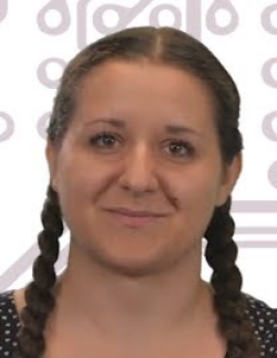
Haubenwallner, Clara

Haubenwallner, Clara
Student Assistant
Graz University of Technology

Haubenwallner, Clara

Abstract
Panelist at Future of Work.

Biography
Clara Haubenwallner is studying Biomedical Engineering at TU Graz. Since 2018, she has been supporting the Institute of Electronics at TU Graz as a student assistant both in teaching and in the creation of digital teaching formats, e.g. ElectrONiX MOOC on iMooX.at as part of the METIS project. In addition, she has experience in the field of talent management through her part-time jobs in the Office for Equal Opportunities and in the Office of Student Counselling.

The Future of Work
H To top
Henkel Corporation Henkel Corporation Trichur, Ramachandran
Semiconductor Packaging Materials Enabling Advanced Flip-Chip and Heterogeneous Integration
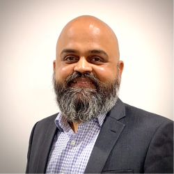
Trichur, Ramachandran

Trichur, Ramachandran
Global Head of Semiconductor Packaging
Henkel Corporation

Trichur, Ramachandran

Abstract
In recent years, semiconductor chip package architectures have become more complex to deliver various applications’ power, performance, size, and cost requirements. Chipsets used in consumer electronics devices such as mobile phones and handheld electronics predominantly require miniaturization, high functionality, low cost, and low power. Therefore, the packages specified for this market segment may include package-on-package (PoP) formats to save space or wafer-level packages (WLP) to deliver lower cost and, in many cases, higher functionality. In comparison, processors used in high-performance computing (HPC) and artificial intelligence (AI) applications place a premium on performance while balancing cost, power, and footprint. Because of these factors, packaging architects have developed several custom package formats like chiplets, large-die flip-chip, and multi-chip packages in 3D and 2.5D, among others. Both end markets require unique innovations in semiconductor packaging materials to enable efficient package production and in-application performance. While package designs have come a long way, challenges to meeting new, demanding requirements persist. Advanced packaging material solutions are central to addressing these issues.Liquid compression molding materials are predominantly used in fan-out or chip-on-wafer packaging for wafer-level encapsulation processes. As the interconnect density or stacking height increases, fine-filler, low-warpage materials are necessary to deliver the package's reliability and the wafer's processability. In AI and HPC applications, the package body size increases with subsequent generations. These large body packages are susceptible to thermal stresses resulting in warpage and reliability concerns. Component level adhesives like lid and stiffener attach materials must be able to manage/prevent warpage while maintaining good adhesion and reliability performance. Lastly, underfills also play a crucial role in packaging logic and memory devices. Pre-applied and post-applied underfill in liquid and film formats are needed to address challenges in flow time, interconnect density, voiding, crack formation, and various other issues. This Keynote will present the latest innovations in encapsulation materials used for fan-out wafer-level molding processes, alongside developments in advanced liquid underfills and lid/stiffener attach materials.

Biography
Coming soon

Advanced Packaging Conference
Holst Centre / TNO Hendriks, Rob
Impulse Printing™: Enabling 3D Printed Interconnects for Volume Production
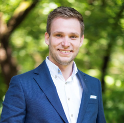
Hendriks, Rob

Hendriks, Rob
Program Lead
Holst Centre / TNO

Abstract
Impulse Printing™ is a brand new technology developed by Holst Centre that will bring unique 3D interconnect solutions to the back-end semiconductor and display market. High resolution structures can be printed over steps, gaps, and even wrapped around substrates at incredible speeds. For example, wrap-around printing of electrodes to create a back-to-front interconnect for µLED displays, or printing directly on silicon dies as an alternative to wire bonding. Off the shelf materials such solder paste, conductive adhesive, silver micron flake ink, copper nanoparticle ink and dielectric ink have already been printed successfully, showing compatibility with a wide range of viscosities and particles sizes. The unique capability of printing almost any materials onto any type of topology makes Impulse Printing™ suitable for quick adoption into existing production lines.

Biography
Program Lead experienced in developing novel printing technologies in the field of hybrid printed electronics. Responsible for defining the overall strategy and leading the execution of innovative technologies, including ultra-high resolution printing, laser-assisted transfer, 3D printed electronics and photonic soldering. Driven by innovation and determined to take concepts to full industrial implementation. Over 10 years of experience working in research and start-up environment across the U.S. and Europe.

Advanced Packaging Conference
I To top
IBM Zurich IBM Zurich Curioni, Alessandro
Keynote Opening
Curioni, Alessandro

Curioni, Alessandro
IBM Fellow, Vice President Europe and Africa and Director IBM Research - Zurich
IBM Zurich

Curioni, Alessandro

Abstract
Coming Soon

Biography
Dr. Alessandro Curioni is an IBM Fellow, Vice President of IBM Europe and Africa and Director of the IBM Research Lab in Zurich, Switzerland. On top of being responsible for IBM corporate research in Europe, he leads global research in Security and the Future of Computing.Dr. Curioni is an internationally recognized leader in the area of high-performance computing and computational science, where his innovative thinking and seminal contributions have helped solve some of the most complex scientific and technological problems in healthcare, aerospace, consumer goods and electronics. He was a member of the winning team recognized with the prestigious Gordon Bell Prize in 2013 and 2015. His reserch interests now include AI, Big Data and novel compute paradigms, such as neuromorphic and quantum computing.Dr. Curioni received his undergraduate degree in Theoretical Chemistry and his PhD from Scuola Normale Superiore, Pisa, Italy. He started at IBM Research – Zurich as a PhD student in 1993 before officially joining as a research staff member in 1998, where he had several research and manager roles, including being the founding manager of the Cognitive Computing and Computational Sciences department. He is a member of the Swiss Academy of Technical Sciences

Smart and Green Manufacturing Summit
imec imec Peeters, Michael
Opening Talk: From Applications to Semiconductors or the other way Around: the Case for Technology-Push
Peeters, Michael

Peeters, Michael
VP of R&D for Connectivity
imec

Peeters, Michael

Abstract
Coming Soon

Biography
Michael Peeters is VP of R&D for Connectivity at imec. His previous experience as CTO for both the Wireline and Wireless business lines at (what is now) Nokia was built on the culture, enthusiasm, and love for technology and science that he got from his time at Bell Labs—and the principles of Free Inquiry bestowed on him by his Alma Mater, the Vrije Universiteit Brussel (VUB).During his research career starting with a Ph.D. in Applied Physics and Photonics from the Vrije Universiteit Brussel, he has authored more than 100 peer-reviewed publications, many white papers and holds patents in the access and photonics domains. An electrotechnical engineer by training, he is a senior member of IEEE and a Fellow of the VUB. Outside of work, his quest to discover the recipe for a perfect lasagna is balanced by bouts of long-distance running to offset the inherent caloric intake.

Future of Computing
ITF Beyond 5G
imec imec Collaert, Nadine
How Heterogeneous Integration Will Shape the Future of Wireless Communications
Collaert, Nadine

Collaert, Nadine
Program Director High-Speed Analog/RF
imec

Collaert, Nadine

Abstract
CMOS has been the technology of choice for many applications because it is easy to manufacture and offers a good balance between performance and cost. However, as we move into the mm-wave and sub-THz frequency spectrum for wireless communications, it is becoming clear that CMOS might not be the best option for all use cases.At these higher frequencies CMOS struggles to deliver the power and efficiency needed, which is where compound semiconductors like GaN and InP come in, especially for the transmit side of the RF Front-End Module (RF FEM).Compound semiconductors have the potential to revolutionize the world of wireless communication, but there are still many challenges that need to be addressed. These technologies are still lacking in maturity. That is why today's research is focused on scaling them up to make them ready for mass volume production. Next to that, they will need to be combined with CMOS delivering the control and calibration for the beamforming architectures. The design of heterogenous platforms enabling this co-integration will therefore be essential to enable the full potential of these solutions for beyond 5G applications. This also calls for EDA tools and methodologies to efficiently partition the system. In this talk we will highlight the current progress towards enabling these hybrid technologies with a focus on 2.5D and 3D integration.

Biography
Dr. Nadine Collaert is program director at imec. She is currently responsible for the analog/RF program looking at heterogeneous integration of III-V/III-N devices with advanced CMOS to tackle the challenges of next generation mobile communication. Before that she was program director of the LOGIC Beyond Si program focused on the research on novel CMOS devices and new material-enabled device and system approaches to increase functionality. She has been involved in the theory, design, and technology of FinFET devices, emerging memories, transducers for biomedical applications and the integration and characterization of biocompatible materials. She has a PhD in electrical engineering from the KU Leuven and she holds more than 400 publications and more than 10 patents in the field of device design and process technology.

ITF Beyond 5G
imec imec De Simone, Danilo
EUV Lithography Patterning: Status and Challenges Towards High NA
De Simone, Danilo

De Simone, Danilo
Staff Member
Imec

De Simone, Danilo

Abstract
Nowadays, the device scaling driven by the Moore’s law is continuing by the deployment of the 0.33NA extreme ultraviolet lithography (EUVL) in high volume manufacturing for single print and multi-patterning schemes further driven by the need to improve cycle time and cost. To further simplify and improve EUV patterning reducing cost and enable 2nm technology and below, high NA EUV lithography is under development and in 2023 imec and ASML will open a high NA EUV Lab, where the first high 0.55NA scanner will be installed.At the same time, as the nanoscale is pushed further down, the stochastic nature of the patterning process becomes one of the major patterning roadblocks. To enable the high NA technology new knobs and faster learning cycles on patterning process development are needed to improve the process window and minimize the stochastic patterning defectivity issues. Lithography solutions can’t afford alone the stochastic challenges; thus, the etching and thin film processes become essential to holistically offer, together with the lithographic process, novel clean pattering solutions. This presentation will show the latest development on EUV patterning materials and their challenges and provide an insight status of overcoming these obstacles towards high NA.

Biography
Danilo De Simone holds a MS degree in chemistry from the university of Palermo (Italy) and has 22 years of experience in semiconductor R&D field. He led the development of lithographic materials for 90nm and 65nm NOR Flash devices for STMicroelectronics (STM) in Italy and covered the role of assignee at STM Alliance in France and STM in Singapore. In 2008, he joint Numonyx to lead the R&D development for lithographic materials and first 32nm double patterning for PCM devices. In 2011, he moved to Micron Technology to introduce 45nm phase-change-memory devices in HVM, and to develop patterning solutions for novel devices. In 2013, he joined the international nanoelectronics research center imec leading the research on patterning materials for EUV lithography. He is editorial board member of the Journal of Micro/Nanopatterning, Materials, and Metrology (JM3), member of SPIE committee for the Patterning Materials and Processes program and member of the International Advisory Board of the Photopolymer Science and Technology Conference (ICPST).

Materials Innovation
imec imec Rolin, Cedric
The Environmental Footprint of Si Chip Manufacturing
Rolin, Cedric

Rolin, Cedric
Program Manager
Imec

Rolin, Cedric

Abstract
The climate crisis calls for urgent actions towards sustainability as an integral component of businesses and regulations. With its large and growing environmental footprint, the Information and Communication Technology sector is arguably a large part of the problem, but also a part of the solution. Fabrication of integrated circuits is an energy and resource intensive process and the drive towards higher performance and increased functionality increases the process complexity dramatically from node to node. Traditionally, the improvement between technology nodes is evaluated using Power, Performance, Area and Cost (PPAC) metrics in a Design Technology Co-Optimization (DTCO) completely neglecting sustainability. However, this established framework provides an opportunity to do early sustainability assessments of future technologies all the way from material sourcing and fabrication to end of life. To demonstrate this approach, we evaluate the environmental impact, more specifically the energy, ultra-pure water (UPW) and mineral consumption as well as the greenhouse gas (GHG) emissions from manufacturing logic, DRAM and NAND technologies from past to future nodes. Our analysis of logic scaling reveals how the environmental metrics normalized per transistor evolve along with improvements in performance and reduction in cell area.

Biography
Cédric Rolin is Manager for the Sustainable Semiconductor Technologies and Systems (SSTS) Program at imec. He received his M.S. degree and his PhD degree in materials science from the Université Catholique de Louvain in 2004 and 2009 respectively. During the first 13 years of his career (including 2 years postdoc at University of Michigan), Cedric grew his expertise in the thin film growth and manufacturing of devices based on organic semiconductors. Then, from 2018 to 2021, he led a R&D team developing solutions to move flexible thin film circuit and display technologies from the Lab to the Fab. Part of this effort focused on the upscaling of the nanoimprint lithography patterning technology to a 300mm Fab tool. Since November 2021, Cédric has joined the sustainability effort of imec as Program Manager, focusing on the assessment and improvement of the environmental footprint of the semiconductor manufacturing industry.

Smart and Green Manufacturing Summit
imec imec Van den hove, Luc
Deep Tech: the Lodestar to Meet the Challenges of the 21st Century
Van den hove, Luc

Van den hove, Luc
President and CEO, imec
imec

Van den hove, Luc

Abstract
Deep tech, enabled by semiconductor technology, will provide disruptive innovations that are essential for tackling humanity's monumental challenges. For example, the world needs a transformation in medicine to address current and future challenges. Many virologists believe that the likelihood of future pandemics is increasing, so we must act now to be prepared for the future. By leveraging the most recent technological advances, we can radically transform medicine to protect the world from future pandemics. Medicine will become digital, enabling vital advancements, including decentralized and low-cost personalized drug and vaccine production. However, the challenges to realizing these critical advancements are enormous. Just as Moore’s law drove the semiconductor industry to respond to increasing computing and storage challenges, we could accelerate medical innovations by a technology roadmap where technology platforms are developed pre-competitively. The transformation of medicine will require the handling and analysis of exponentially growing amounts of data, demanding enormous computing power. And healthcare is just one of the many new application areas which will depend on the exponential growth of data. To enable this sustainably, we need an even more aggressive semiconductor roadmap than what we have achieved over the last decades. At imec, we have proposed a roadmap on how we can continue to enable more performant semiconductor technologies. And we will leverage our core semiconductor expertise to realize deep-tech innovations by co-innovating at the semiconductor technology level, the system and application levels, and by leveraging expertise from many domains such as material science, biomedical, pharma, AI, and others. Building flourishing deep-tech ecosystems must become a priority to meet the challenges of the 21st century.

Biography
Luc Van den hove is President and CEO of imec since July 1, 2009. Before he was executive vice president and chief operating officer. He joined imec in 1984, starting his research career in the field of silicide and interconnect technologies.In 1988, he became manager of imec’s micro-patterning group (lithography, dry etching); in 1996, department director of unit process step R&D; and in 1998, vice president of the silicon process and device technology division. In January 2007, he was appointed as imec's EVP & COO. Luc Van den hove received his PhD in electrical engineering from the KU Leuven, Belgium.He has authored or co-authored more than 200 publications and conference contributions.

Executive Forum
imec imec Marent, Katrien
Welcome
Marent, Katrien

Marent, Katrien
EVP & Chief Marketing and Communications Officer
imec

Marent, Katrien

Abstract
Coming Soon

Biography
Katrien has an engineering degree in microelectronics. She joined imec in 1992 as analog design engineer and specialized in design of low-noise readout electronics for high-energy physics. In 1999, she became press responsible and scientific editor at imec's business development division and was responsible for authoring and editing the research organization's numerous company technical documents and publications. In 2001, she was appointed corporate communications director at imec. Her responsibilities expanded in August 2007, when she got the position of external communications director including corporate, marketing and outreach communications. In October 2016, she became VP corporate, marketing and outreach communication. Since April 2020 she is Executive Vice President & Chief Marketing and Communications Officer and member of the executive board of imec.

ITF Beyond 5G
imec imec Altamirano-Sanchez, Dr. Efrain
Towards Sustainable Wet Processing for Advanced Integration Technologies
Altamirano-Sanchez, Dr. Efrain

Altamirano-Sanchez, Dr. Efrain
R&D Manager of SIP group
imec

Altamirano-Sanchez, Dr. Efrain

Abstract
The new challenges for wet processing are associated with the new materials and the scaling roadmap for Logic, Memory, and 3D system integration (STCO) i.e CFET, 3D Memory, D2W, W2W, and FOWLP. The specifications for defects, pattern-collapse, selectivity, and uniformity will be tighter and tighter, demanding more advanced hardware and formulated chemicals. One challenge for the cleaning community will be how to contribute to maximizing the wet processing performance and the cost-benefit. In the Semiconductor industry, wet processes are more and more critical but also resources intensive in energy, water, and chemicals. Hence, another big challenge ahead for the cleaning community is how to minimize GHG emissions and abide by the announced targets for net-zero carbon emissions by 2050. In this paper, examples of the above-mentioned technologies and the related wet processes will be discussed.

Biography
Dr. Efraín Altamirano-Sánchez holds a Ph.D. in Chemical Engineering. He joined imec in 2006 where he developed strong expertise in advanced patterning for technologies nodes ranging from 65 nm to 5 nm. In 2018, he joined the wet processing team as a group manager. He is now focused on the innovation of wet process solutions for CFET, 3D DRAM, 3D integration & sustainability.

SCREEN
imec the Netherlands imec the Netherlands Zevenbergen, Marcel
Panelist
Zevenbergen, Marcel

Zevenbergen, Marcel
program manager
imec the Netherlands

Zevenbergen, Marcel

Abstract
N/A

Biography
Dr. Marcel Zevenbergen obtained his MSc from Delft University of Technology in 2005 and a PhD from the same university in 2009. Afterwards, he joined imec the Netherlands where he developed novel sensor platforms for various applications, in close collaboration with industrial partners. Current position is program manager both at imec@HolstCentre and imec@OnePlanet leading the advanced sensor development for various applications ranging from precision agriculture and food production, water quality and bioprocessing monitoring.

Smart MedTech
INFICON INFICON Behnke, John
The Digital Transformation of Semiconductor Manufacturing
Behnke, John

Behnke, John
General Manager FPS
INFICON

Behnke, John

Abstract
Coming Soon

Biography
Mr. Behnke has more than 35 years of semiconductor industry experience including: logic and memory manufacturing, technology/product development and fab operational excellence. As the GM of Final Phase Systems an INFICON Product Line, John leads a team that develop and deploy SMART software solutions that enable fabs to improve their manufacturing efficiency. FPS’s suite of software solutions are built upon a common Datawarehouse which enables advanced Fab Scheduling and optimized WIP movement as well as other related capabilities. He is also a Co-Chair of the Semi North America Smart Manufacturing Special Interest Group. Prior to FPS John served as the CEO and President of Novati Technologies, the SVP and GM of the Semiconductor Group of Intermolecular, the CVP for Front End Manufacturing, Process R&D and Technology Transfers at Spansion and the Director of AMD’s Fab 25’s Engineering and Operations groups where he was a founding member of AMD’s Automated Precision Manufacturing (APM) initiative which led the Semiconductor industry’s development and use of APC and other advanced factory systems. He also led the successful conversion of Fab 25 from Logic to Flash memory which was enabled through the virtual automation of the fab.Mr. Behnke earned a B.S. degree in Mechanical Engineering with an Industrial Engineering Minor from Marquette University. Mr. Behnke holds five U.S. patents.

Fab Management Forum
Infineon Infineon Knott, Bernhard
Innovative Sensor Packaging in Europe
Knott, Bernhard

Knott, Bernhard
Head of the Infineon Technologies Backend Innovation Group
Infineon

Knott, Bernhard

Abstract
The presentation will include topics like: eWLB radar (fan-out WLP at Infineon Regensburg); Pressure sensors e.g. for automotive; Magnetic sensors and Gas sensors.

Biography
Bernhard Knott is the Head of the Infineon Technologies Backend Innovation group. He is responsible for new Package Concepts, Prototyping, new Materials, Simulation and Virtual Prototyping. Until 2016 he was leading the Package Development for Sensors and Waferlevel Package Development in Regensburg, Germany. Prior joining the Backend Organization, he held several Management Position in Frontend Technology dealing with BiCMOS Technologies, Sensors and Innovation projects. After receiving his Diploma in Physics from the University of Regensburg, he started his career in Semiconductor Industry in 1997 in developing an embedded NVM Technology. Bernhard holds several patents and patent applications in the area of FE Technology, Sensors and Packaging.

Advanced Packaging Conference
Infineon Technologies AG Infineon Technologies AG Stöckl, Martin
Talent & Skills
Stöckl, Martin

Stöckl, Martin
Senior Vice President / Global Head of HR People and Organization Effectiveness
Infineon Technologies AG

Stöckl, Martin

Abstract
Talent situation, strategic talent demand, cooperation requirements between academia, economy and government to assure talents and attractiveness of the location

Biography
Education›General Management Program (Harvard Business School)›M.Sc. Management & Organization Analysis (Warwick Business School)›B.Sc. Business PsychologyInfineon:•2019 – now: Senior Vice President - Global Head of People & Organization Effectiveness•2018 – 2019: Vice President - Global Head of People & Organization Effectiveness•2017 – 2018: Senior Director - Head of Organization, Culture & ChangeDeloitte ConsultingAccenture Strategy

The Future of Work
Infineon Technologies AG Infineon Technologies AG Recklies, Joerg
Opening Remarks by Session Chair
Recklies, Joerg

Recklies, Joerg
Senior Vice President
Infineon Technologies AG

Recklies, Joerg

Abstract
No Content

Biography
Joerg Recklies has been in the semiconductor industry for 27 years with responsibilities ranging from Chip design to IDM. He is currently in charge of the General Manager at Infineon Technologies Regensburg. Prior to that, Joerg Recklies was in charge of the FAB Manager at Infineon Dresden and held several positions in automation and productions at Infineon. These positions contributed to his excellent experience in terms of equipment and automation. Earlier in his carrier he has made contributions in digital and analog Chip design.Joerg Recklies holds a graduate engineer for Semiconductor.Highlight during the time with Infineon …. - Establish high automation at IFD 1995- 1997 as project leader automation software integration- Project Leader world wide cost reduction program within Infineon Frontend Productions from 1999 –2003 (within Europe, US, Asia)- Section Manager Plasma Etch / Wafer Inspection 2003- 2007- Director Maintenance Engineering 2007 – 2014- Project Leader 300 mm Fab Startup / Transfer Power Technologies 2011-2013- FAB Manager Senior Director 200 / 300 mm Dresden 2014 – 2018- General Manager Site Regensburg Senior Vice President since 2018

Fab Management Forum
Infineon Technologies AG Infineon Technologies AG Gorski, Alexander
Panelist
Gorski, Alexander

Gorski, Alexander
Executive Vice President, Back-End Operations
Infineon Technologies AG

Gorski, Alexander

Abstract
Coming Soon

Biography
Alexander is responsible for Infineon Technologies AG’s global back-end operations cluster which combines all in-house and external manufacturing. The in-house manufacturing footprint consists of 11 sites located all around the world. In his role as Cluster Head, he is also in charge of package innovation, test technology development as well as manufacturing automation and digitalization. Previously, Alexander was a Board Member of Infineon Technologies AG’s Power & Sensor Systems Division. Serving different global markets in power management and sensor systems, such as computing, consumer, industrial, and automotive, the division holds a leading position in a variety of applications. In his role as Division Chief Operating Officer, Alexander has overseen global operations as well as technology, innovation, and software. Before re-joining Infineon in November 2016, Alexander served for almost a decade as a Member of the Management Board and Group COO at Conergy, a leading global renewable energy company focused on solar. During his tenure, he was instrumental in helping the company transition from a solar component manufacturer into a fabless and asset-light project development and turnkey EPC company.Alexander started his professional career in the semiconductor industry at Siemens Semiconductor, later carved out as Infineon Technologies. During his time with Siemens and later Infineon, he served in several management positions in operations, supply chain, and key account management. Alexander holds an MBA from the University of Regensburg, Germany.

ATREG PANEL
Infineon Technologies AG Friedrichs, Peter
SiC Power Technologies and Business – Empower a Greener Future

Friedrichs, Peter
Vice President SiC
Infineon Technologies AG

Abstract
SiC power devices have shown a tremendous growth over the last few years, targeting to a multi-billion dollar business by the end of the decade. Many driving applications belong to the segment of emerging applications related to the electrification of mobility and enhanced use of green energy. Those new applications, however, might need device solutions which differ substantially from the known portfolio based on silicon. One trend is for instance a much wider range of rated blocking voltages in order to be more application specific. The presentation will explain this trend in more detail and give concrete examples how such an adapted portfolio impacts the future of wide band gap power semiconductors.

Biography
Dr. Peter Friedrichs received his Dipl.-Ing. in microelectronics from the Technical University of Bratislava in 1993and his Ph.D work at the Fraunhofer Institut FhG-IIS-B in Erlangen. His focus area of expertise was the physics of the MOS interface in SiC. In 1996 he joined the Siemens AG and was involved in the development of power devices on SiC.Peter joined SiCED GmbH & Co. KG, a company being a joint venture of Siemens and Infineon, on March the 1st, 2000. Since July 2004 he was the managing director of SiCED. In 2009 he achieved the Dipl.-Wirt.-Ing. From the University of Hagen. After the integration of SiCED’s activities into Infineon he joined Infineon on April 1st, 2011 and acts currently as Vice President SiC.

Electrification & Power Semiconductors
Infineon Technologies AG Infineon Technologies AG Fros, Agnes
Infineon and Lam Research: Machine Learning will Change the Way We Work - A Collaboration to use Big Data Analysis and Regression Modeling to improve Fab Productivity and to Lower Manufacturing Costs
Fros, Agnes

Fros, Agnes
Director
Infineon Technologies AG

Fros, Agnes

Abstract
Infineon views Artificial Intelligence/Machine Learning (AI/ML) as the foundation to the development of novel techniques leading to improved product performance and fab stability, whilst at the same time being a key driver of competitiveness. AI empowers the engineer to focus less on data acquisition and more on the analysis. When this is coupled with experience acquired in the fab, real opportunities to increase stability, increase yield, and lower costs become apparent to engineers in ways they did not before. AI can reduce the burden of decision-making in the fab when predicted outcomes are consistent with actual outcomes. In this context, the cost and productivity challenges posed by metrology in the fab environment clearly present an opportunity for improvement.This presentation describes the collaboration between Infineon and Lam Research to improve costs and efficiency of the etch rate qualification and reports the results achieved.Equipment Intelligence® data analysis (EI-DA) is a proprietary advanced multivariate big data analysis system developed by Lam Research. EI-DA polls the entire sensor matrix on Lam 2300® platforms, distilling large quantities of data through dimension reduction techniques. A novel approach, so called ‘virtual metrology’, leverages EI-DA, to seek process specific statistical parameters which best map ‘in process’ performance to on-wafer results in an accurate and repeatable way. Employing the principles of ML, the predictive models are periodically fed real on wafer data (‘y-data’), to validate the results. Through further extension of this method, Lam and Infineon have demonstrated consistent performance of the models when applied to the more cost effective ‘bare silicon’ wafers. This enables lower material cost, reduced utilization of metrology tools, and higher fab productivity.Predictive model fitting of R²≈0.87, (RMSE≈0.5) has been demonstrated, which is consistent with real on wafer data. The model reliability offers Infineon the option to selectively replace conventional metrology operations with virtual metrology. Additionally, the method allows a metrological result to be predicted with a high degree of confidence for every wafer. Much of the decision-making process becomes automated. Solutions are arrived at earlier. Such successful applications of AI/ML enable better approaches to how we work today, and into the future, in line with the Infineon vision of “Being part of today, Being part of tomorrow”.

Biography
Agnes Fros has 12 years of experience in the semiconductor industry. After her degree in Industrial Engineering for physical technologies at the University of Münster, Agnes joined Infineon Regensburg where she completed the certified Innovation Manager program at Sensorik Cluster. In the Frontend divisions she has held many roles including Performance Controller, Industrial Engineer, Defect Density Engineer and Process Integration Engineer for HF products. Under her leadership of the Wafer Inspection and automated Optical Outgoing Inspection departments, superior quality for all products processed was delivered. Since 2020 Agnes Fros is Director of the Plasmaetch Department for Frontend Production, responsible for both process engineering and the maintenance of an extensive fleet of Fab tools. By applying novel AI techniques to the existing fab knowledge base in Infineon, Agnes Fros is leading an effort to automate decision making processes in the fab for better and more consistent outcomes.Co-presenterOttaviano Zechini, Sr, Director, Europe Equipment Intelligence Leader, Lam Equipment Intelligence Zechini holds a masters degree in Electronic Engineering and has more than 25 years’ experience in the semiconductor business, working for leading equipment manufacturers such as GaSonics, Novellus Systems and Lam Research, starting from Operations Management, moving to Sales Management and then to Account General Management. He joined Lam Research in 2015 as a Site GM based in Dresden, to then be appointed as Central Europe Account GM in 2017. Since January 2022, he has been leading the Lam Equipment Intelligence® activities within the European Region.< !--EndFragment -- >

Fab Management Forum
Institute of Electronics and Computer Science Institute of Electronics and Computer Science Ivanovs, Maksims
Synthetic Data for Robotics: Opportunities and Challenges
Ivanovs, Maksims

Ivanovs, Maksims
researcher
Institute of Electronics and Computer Science

Ivanovs, Maksims

Abstract
To successfully operate in a real-world environment, robotic systems need to demonstrate high speed, precision, adaptability, and interoperability. Machine-learning based perception modules of robotic systems require a lot of training data, as state-of-the-art deep learning techniques are well-known as particularly data-hungry. Moreover, the training data should ideally come from a broad distribution to cover corner cases as well as be adaptable to new deployment scenarios. As collecting and labelling real-world data is time- and effort-consuming, the use of synthetic data in robotics has gained increasing attention, as this promising and rapidly developing approach allows to generate large amounts of the data and apply modifications to them as needed. The main challenge to the wide-scale application of synthetic data in robotics is the gap between the simulation and the real world, which often results in the decrease in the precision of the systems trained solely on the synthetic data. One of the ways to bridge this gap is to transfer the style from the real-world data, which are realistic in appearance yet limited in number, to the less-realistic but plentiful synthetic data. In our recent study, we demonstrated how that can be accomplished by means of particular deep neural networks, Generative Adversarial Networks (GAN); as a result, we achieved an improvement of object detection on a bin-picking task, one of the major tasks in industrial robotics.

Biography
Maksims Ivanovs is a researcher at the Institute of Electronic and Computer Science (EDI) at Riga, Latvia, and a PhD student and acting lecturer at the University of Latvia. He is working on the topic of generating synthetic data for training deep neural networks under the supervision of Dr. sc. ing. Roberts Kadiķis (EDI), and his academic interests are mostly related to deep learning and artificial intelligence in general as well as to the impact of these fields on society.

Chips Hub Europe
Intel Corporation Intel Corporation Scheper, Frans
Building Europe’s Digital Future - A Pan European Investment
Scheper, Frans

Scheper, Frans
Corporate Vice President in the Sales and Marketing Group General Manager and President EMEA
Intel Corporation

Scheper, Frans

Abstract
This keynote will explore the European digital landscape and what challenges and opportunities it presents for the semiconductor industry. Frans will examine the macro opportunity across the region, touching on geopolitical issues,supply chain disruptions, and the potential of the 2030 Digital Compass. He will provide an overview of how Intel has reacted to the market landscape including a deep dive into the once in a generation investment across the EU inorder to diversify the global semiconductor supply chain. Finally, he’ll touch on what this digital transformation means for Europe, Middle East and Africa’s industries, including telecoms, education, and government, with a deep dive onthe automotive sector.

Biography
Frans Scheper is Corporate Vice President in the Sales and Marketing Group General Manager and President, for Europe, Middle East and Africa (EMEA) for Intel Corporation.Frans is responsible for Intel’s overall business in EMEA which includes driving revenue growth, engaging with the local ecosystem to create new opportunities, and strengthening Intel’s existing regional customer and partner relationships.As President, Frans oversees Intel’s recently announced plans for the “once-in-a-generation” investment in Europe as part of its IDM 2.0 strategy, with research, design, leading-edge semiconductor manufacturing and industry partnerships that will help build Europe’s digital future.Frans recently joined Intel (2022) from ams OSRAM, where he was Chairman and Executive Vice President of Opto Semiconductors. He brings extensive European and international market experience, having also held executive board positions at WeEn Semiconductors, NXP Semiconductors and the CEO position at Nexperia.Based in the Netherlands, Frans holds a bachelor’s degree in business and commerce from HES Den Haag, and an MBA from the International Institute for Management Development (IMD).

Advanced Packaging Conference
Intel Germany GmbH & Co. KG Intel Germany GmbH & Co. KG Mohr, Anneclaire
Net-Zero: A Call to Action for the Semiconductor Industry
Mohr, Anneclaire

Mohr, Anneclaire
Managing Attorney, Business, Regulatory and Sustainability Legal (Europe, Middle East and Africa)
Intel Germany GmbH & Co. KG

Mohr, Anneclaire

Abstract
Intel will share its commitment and progress toward net-zero greenhouse gases (GHGs) and outline the key challenges ahead for the semiconductor industry and opportunities to work together toward a net-zero future.

Biography
Anneclaire is a senior attorney providing legal support in the fields of product regulations, environmental laws and sustainability in EMEA. She joined Intel in 1997 and focused in the last ten years primarily on product regulatory and environmental legislation, as well as, more recently, emerging sustainability legislation closely related to ESG disclosure, reporting and responsible business conduct. Anneclaire studied law at the Robert Schuman Law University of Strasbourg, France, and graduated from the Institute of Political Studies of the Robert Schuman University, Strasbourg.

Smart and Green Manufacturing Summit
iPronics, Programmable Photonics Capmany, Jose
Silicon Programmable Photonics: A New Paradigm to Unleash the Power of Lighwave Chips
Capmany, Jose

Capmany, Jose
Co-Founder
iPronics, Programmable Photonics

Abstract
This talk will address the foundations, operational principles and applications of programmable silicon photonics leading to the concept of general purpose processors and Field Programmable Photonic Gate Arrays. Recent progress made by ipronics and other players on the development of hardware, control electronics and software layers will be reviewed and future directions of research and development.

Biography
Dr. Dr. José Capmany is a Full Professor in Photonics and leader of the Photonics Research Labs (www.prl.upv.es) at the institute of Telecommunications and Multimedia Applications (www.iteam.upv.es), Universitat Politècnica de Valencia, Spain. He holds BSc+MSc degrees and doctorates in Electrical Engineering and Physics.He has published over 600 papers in international refereed journals and conferences and has been a member of the Technical Program Committees of the European Conference on Optical Communications (ECOC), the Optical Fiber Conference (OFC). He is a Fellow of the Optical Society of America (OSA) and the Institute of Electrical and Electronics Engineers (IEEE. He is also a founder and chief innovation officer of the spin-off companies VLC Photonics (acquired by Hitachi in 2020) dedicated to the design of photonic integrated circuits and iPronics (www.ipronics.com) dedicated to programmable photonics.Professor Capmany is the 2012 King James I Prize Laureate on novel technologies and the National Research award in Engineering 2020, the two highest scientific distinctions in Spain, for his outstanding contributions to the field of microwave photonics. He has also received the Engineering achievement award from the IEEE Photonics Society and the Innovation prize from the Royal Society of Physics in Spain. He is an ERC Advanced and Proof of concept grantee and was a distinguished lecturer of the IEEE Photonics Society for the 2013-14 term. Associate Editor of IEEE Photonics Technology Letters (2010-2016) and the IEEE Journal of Lightwave Technology (2016-2018). He served as Editor in Chief of the IEEE Journal of Selected Topics in Quantum Electronics from 2018 to 2022.

Integrated Photonics
IQE plc IQE plc Pelzel, Rodney
How Advanced Epitaxy is Critical to making the Semiconductors for Next-Gen Mobile Connectivity

Pelzel, Rodney
CTO
IQE plc

Pelzel, Rodney

Abstract
The epitaxy process is the most critical and demanding step in the RF semiconductor manufacturing chain. In this presentation, we’ll discuss the role of advanced epitaxy for RF to 5G and beyond, including higher frequencies up to 300 MHz, and highlight different materials (III-V, silicon, and germanium). We’ll look at how IQE sees the market trends and needs, which applications are the most demanding, and how IQE is innovating – for example, how the development of InP epiwafer HBT and HEMT structures has enabled our customers to develop transceiver chipsets with world-class performance. We’ll look ahead at how IQE sees its role in the future ecosystem, what are the biggest challenges, and where technology innovation in epitaxy will take us.

Biography
Dr. Rodney Pelzel has over 20 years of experience in the semiconductor industry, with deep expertise in semiconductor materials engineering and the epitaxial growth of compound semiconductors. Dr. Pelzel joined IQE as a Production Engineer in 2000. For the first twelve years of his career with IQE, Dr. Pelzel held various engineering and operational management roles focusing on scaling leading-edge epitaxial technology for volume manufacturing for wireless applications. In 2012, Dr. Pelzel was appointed as the head of R&D for the IQE Group and was tasked with creating unique materials solutions that enable IQE’s customers and provide them with a competitive edge. Throughout his career, Dr. Pelzel has been involved in numerous new product introductions, the most recent being IQE’s highly successful launch of 6” VCSELs for consumer applications. Dr. Pelzel is a chemical engineer by training, holding a BS (High Distinction) from the University of Colorado (1995) and a Ph.D. from the University of California, Santa Barbara (2000). He is a Chartered Engineer and a Chartered Scientist, and a Fellow of the Institution of Chemical Engineers. Dr. Pelzel’s work has been widely published and he is the co-inventor of 30+ patents.

ITF Beyond 5G
ISRL ISRL Zabelinsky, Ilya
Time to Collaborate. SubFAB Research and Development
Zabelinsky, Ilya

Zabelinsky, Ilya
Co-Founder
ISRL

Zabelinsky, Ilya

Abstract
The ChallengeThe Semiconductor Industry’s desire for sustainable manufacturing has many challenges to overcome before environmental targets set by most companies can be trustfully met with meaningful positive impact on Global climate changes.One of the key areas poised to become a showstopper for the industry’s ability to achieve sustainability goals is commonly called SubFAB. The SubFAB is a variety of equipment and technologies designed to handle process materials from tool chambers to the factory’s exhaust stacks.Existing infrastructure and siloed approach for SubFAB equipment and technologies R&D can’t support true game changing development of environmentally friendly and affordable solutions to match the manufacturing technologies advancement cadence.This sector is traditionally underserved by fundamental academic research and typically fails to compete for Fab equipment downtime, especially these days when chips shortage keeps factories fully loaded.Chipmakers are forced to spend more capital money on manufacturing capacity and face skyrocketing operational costs. Equipment manufacturers are struggling to meet customer requirements for equipment uptime and Hazadous Air Polutant (HAP) emissions. At the same time academic institutes aren’t involved in research of chemistry and physical nature of post-process material handling.The OpportunityInternational SubFAB Research Labs (ISRL) strategic initiative is being formed these days to pull in an industry-wide collaborative effort on a mission to Bring the Science to SubFAB” and supplement Semiconductor manufacturing technologies advancement with focused research of unwanted and harmful side effects caused by unreacted process materials downstream from process chambers.Member companies will gain access to dedicated facility with complete infrastructure required to operate a set of 300mm process tools with versatile setup of deposition and dry etching process chambers at HVM-like conditions to supplement research and development projects.ISRL will provide its partners a unique opportunity to participate in fundamental research and gain access to common IP or alternatively invest in development of company specific solutions with compartmentalized IP.ISRL will have highly skilled project teams to lead scientific research focusing on reliability issues, technology validation, pathfinding, materials handling and reclaim. Facilities setup will enhance practical skills acquisition for workforce development.

Biography
Ilya Zabelinsky is a globally recognized Technical Leader with over 25 years of experience in vacuum and gas abatement applications for Semiconductor manufacturing.Ilya joined Intel in 1996 to take part in startup and commissioning team of first 200mm fab in Israel, moving on to develop his career as operational and technical leader through several technology node transitions and manufacturing capacity expansion projects. In 2006 Ilya spearheaded an effort to install and commission a full set of vacuum and gas abatement systems for a greenfield construction of 300mm Fab in Kiryat Gat, extending his operational and technical leadership to entire SubFAB ecosystem supporting technology transitions and capacity expansion projects from 45 to 10nm.In April 2022 Ilya left Intel on a mission to “bring the Science to SubFAB” by supplementing Semiconductor manufacturing technologies advancement with focused research of unwanted and harmful side effects caused by unreacted process materials downstream from process chambers.In May 2022 Ilya co-founded International SubFAB Research Labs (ISRL).Ilya possesses broad knowledge and vast practical experience in wide range of semiconductor manufacturing processes, FAB equipment, central facilities systems and infrastructure, spanning from scope definition, programming and design through construction, commissioning and operations. Ilya holds a B.Sc in Chemical Engineering from SCE, Israel. Ilya is passionate practitioner of various education and mentoring programs aimed at new generations of professional and diverse workforce.

Innovation Showcase
ITEC B.V. ITEC B.V. Patschkowski, Felix
Smart Test Cells: Improving Efficiency and Convenience
Patschkowski, Felix

Patschkowski, Felix
Principal Software Engineer
ITEC B.V.

Patschkowski, Felix

Abstract
While testing is the quality gate assuring that only good products go to the customer it does not improve the product and thus must be as efficient as possible. Test setups (Test Cell) comprise more and more equipment types (wafer probers, final test handlers, laser markers, vision inspection systems, automatic reel changers, AMHS’, testers, …). Typically testers have the longest lifetime in the test cell, especially if they are not the bottleneck equipment that slow the overall setup down. ITEC will showcase how a test cell can be automated and integrated when the tester becomes the master equipment including wafer map handling and post processing like DPAT and Maverick Wafer Handling in order to increase the output.

Biography
Before migrating to the Netherlands, Felix Patschkowski graduated from the Technical University of Hamburg with a master’s degree in computer science and engineering and started as an automation engineer at Nexperia’s wafer fab in Hamburg. Being responsible for the automation of the wafer test department, he was exposed to ITEC’s technology, especially the tester platforms, right from the beginning. On a business trip to Nijmegen, he fell for the city and technology. Soon after, he started working for ITEC to develop software for existing and new testers. Over time, he grew into the position of a software architect for the latest test platform under development – the MegaParset. Next to his career he is also active in Olympic saber fencing.

Chips Hub Europe
J To top
JCET JCET Antonicelli, Roberto
New Trends in Mobility and Automotive Semiconductor Industry: a Supply-Chain Perspective
Antonicelli, Roberto

Antonicelli, Roberto
Automotive BU
JCET

Antonicelli, Roberto

Abstract
Coming Soon

Biography
Roberto Antonicelli is a professional with over 20 years of experience in the semiconductor industry. At JCET Group, formerly STATS ChipPAC, he is in charge of the Automotive BU for US and Europe. He is based in Morges (Switzerland), on the shores of the Leman Lake. Prior to joining STATS ChipPAC in 2010, he has held diverse R&D positions at Infineon Technologies, Alcatel Microelectronics and ST Microelectronics. Roberto obtained his MSEE and PhD from Polytechnic University of Bari, Italy, respectively in 1997 and 2002.

Advanced Packaging Conference
Smart Mobility
JCET JCET Azzopardi, Mark
HFBP as a New and Better Approach to DFN
Azzopardi, Mark

Azzopardi, Mark
Business Development Engineering
JCET

Azzopardi, Mark

Abstract
Coming Soon

Biography
Mark Azzopardi has been building semiconductor packaging experience for just over 20 years, after getting his Engineering degree in Mechanical engineering from the University of Malta in 2002. He started his career as a process engineer and moved to R&D for SiP and MEMS packaging. Mark then joined Statchippac, now JCET, in 2011 as technical program manager and moved to Business Development supporting the European local sales team early 2022.

Advanced Packaging Conference
JCET Group JCET Group Choon Heung, Lee
Complex, Small, Cheap: How Packaging is Going to Power the Digital Age
Choon Heung, Lee

Choon Heung, Lee
Chief Technology Officer
JCET Group

Choon Heung, Lee

Abstract
The relentless penetration of increasingly efficient smartphones, high-performance computing, autonomous driving, and artificial intelligence has scaled up the complexity of a wide range of mainframes, desktops, handhelds, and wearable devices. At the same time, the persistent quest for performance, mainly in terms of speed, accuracy, and power consumption, has been constantly pushing the limits of semiconductor technology and silicon transistor nodes in an unprecedented way. Requirements for miniaturization and economy of scale have long prevailed with the astonishing result that many billions of transistors can today be packed into a space no larger than a few square centimeters at the cost of a sandwich.While the past decades were excellent in terms of industrial efficiency and economic return for the semiconductor segment, the years ahead look more challenging in these regards. In recent years, the semiconductor industry has been exposed to severe restrictions in sustaining the classic “Moore-driven” approach to the design and manufacturing of large monolithic chips. Limitations in wafer size, reticle size, transistor density, and the rising cost of advanced silicon nodes have driven the industry to rethink the way complex microchips are designed, manufactured, and tested.Research and investments in advanced semiconductor packaging, under the leading efforts of major assembly and test houses, are offering today new instruments for high-performance, small-form-factor, and cost-aware solutions that were unimaginable a few years ago. Heterogeneous integration, for example, allows a more efficient design and manufacturing process to assemble and test sub-parts and sub-systems, from chiplet to chipset, to modules. Smarter and more sustainable supply-chain schemes can be made compliant with a new range of performance indicators, such as interconnect density, scalability, reusability, and silicon node matching, with substantial advantages in terms of cost.This presentation focuses on the recent developments in terms of advanced semiconductor packaging and, in particular, the heterogeneous integration solutions available in the industry for complex, miniaturized, and cost-sensitive systems for smartphones, high-performance computing, automotive, and other applications where intense computing and artificial intelligence are required.

Biography
Dr. Lee Choon Heung joined the company as Chief Technology Officer on May 17, 2019. Prior to joining the company, Dr. Lee served as Chief Technology Officer and Executive Vice President for Worldwide Manufacturing Operations at Amkor Technology, and President of Amkor Korea. Dr. Lee holds a Master's degree in Solid State Physics and a Ph.D. in Theoretical Solid State Physics from Case Western Reserve University. He has written numerous research papers on various packaging technology related subjects and was granted 38 patents in Korea and 21 patents in the US.

Executive Forum
K To top
KLA Corporation (SPTS Division) KLA Corporation (SPTS Division) Wood, Alex
Plasma Etch & Deposition Processes for SiC Devices in Power Applications

Wood, Alex

KLA Corporation (SPTS Division)

Wood, Alex

Abstract
SiC is a key enabler for high power devices required for end applications such as electric vehicles (EVs), power infrastructure, and wind energy. According to Yole, the SiC power device markets will reach $6.3B by 2027 at a CAGR from 2021-2027 of 34%. The market for SiC power devices for EVs alone is forecast to grow from $685M in 2021 to almost $5B in 2027[1]. Currently, volume production of power devices at 100mm and 150mm wafers is “the norm”, but several power device manufacturers are now progressing to realize the cost benefits of scaling to 200mm wafer formats.This presentation will discuss how Sigma® fxP physical vapor deposition (PVD can be used to deposit on SiC wafers at ≤200mm, for both front-side and back-side metallization. The presentation will give details of how SPTS Sigma® PVD technology overcomes various challenges which can affect yields in SiC power device manufacturing, including eliminating whiskers during thick metal deposition, avoiding contamination, active-face protection and stress control.We will also review etch process and hardware solutions used in the manufacture of SiC power devices. These will include hard-mask open and shallow SiC trench etching and SiC dicing. End-point detection, an essential method of process control, will also be discussed.[1] Yole Développement, "Power SiC 2022”(March 2022)

Biography
Alex Wood is a PVD Product Manager in the SPTS division of KLA Corp, with over 8 years’ experience in the semiconductor manufacturing industry. They joined SPTS in 2013 as an R&D Accounts Etch Graduate Process Engineer, before moving to a Senior Process Engineer position, focussing on the development of frontside SiC power and AlScN processes. Alex transferred to PVD Product Management in 2021 and has been supporting SPTS’ customers in several markets, such as Power and RF.

Electrification & Power Semiconductors
Koh Young Europe GmbH Koh Young Europe GmbH Lindloff, Axel
Applying 3D Moiré interferometry measurement to semiconductor packaging applications

Lindloff, Axel

Lindloff, Axel
Senior Process Specialist Pre-Sales
Koh Young Europe GmbH

Lindloff, Axel

Abstract
The presentation will highlight the benefits using 3D Moiré Interferometry in Packaging applications. From wafer-bumping to advanced wafer-level packaging the Moiré Interferometry provides high accuracy and a common solution for a 100% 3D measurement of the substrates. What are the differences to common 3D measurement systems in SMT and backend? And what are the applications where this technology can be used? Due to the component shortage in electronic industry and the dependency on Asian suppliers, the European Community decided to double Europ’s global market share in Semi-Conductor industry to 20% in 2030. This requires huge investments in new production and research capacities. To achieve this goal, the EU launched at the 8th of February 2022 “The European Chips Act”, which will mobilise €43 billion Euros of public and private investments. At the same time, we see a trend to a multi-chip packaging process. Moore’s Law is not valid anymore. The effort to develop smaller structures is too high, but the opportunities and benefits in combining different chips and components in one package are promising. Complex functions of whole devices can be integrated into a small BGA or IC package. This trend affects all packaging processes from 2D via 3D down to wafer-level packaging. The packaging process is getting more complex and challenging, but new interconnection methods like hybrid-bonding and interposer materials allowing a higher density and integration level. Smaller components, higher density and new materials are challenging the existing inspection and measurement systems. Tailored measurement devices are required to support the new packaging trends. Especially, when the boundaries between front-end and back-end applications or back-end and SMT are blurring. 3D Moiré Interferometry measurement is the recent standard in SMT. Due to the proofed robustness and reliability of this measurement these machines are used in semi-conductor packing since several years. The pesentation will show the adaptation of the well-known Moiré Interferometry principal in SemiCon and packaging applications.

Biography
Axel Lindloff studied general electrical engineering at the Bielefeld University of Applied Sciences and has been active in the SMT world since 1999. He initially gained 3 years of experience in sales of stencils and consumables before moving to the application department of a well-known printing machine manufacturer in 2003. Here he worked until 2012 with the optimization of existing processes, audits and the development of new printing applications. Since September 2012 Mr. Lindloff has been working for Koh Young Europe GmbH as a process specialist for SMT manufacturing. Here he mainly deals with questions relating to solder paste printing, semi-conductor, conformal coating and process optimization with the 3D data obtained.

Advanced Packaging Conference
Kontron-AIS GmbH Kontron-AIS GmbH Mueller, Bert
Sensor Integration Framework with Interface A
Mueller, Bert

Mueller, Bert
Head of Business Unit System Integration
Kontron-AIS GmbH

Mueller, Bert

Abstract
Within the last few years, semiconductor, photovoltaic or HB-LED industry developed enormously. With the result that the complexity of almost all relevant processes increased. To prevent the increase of corresponding costs, a concept of Equipment Engineering Systems (EES) is essential. Integrating applications like Equipment Data Control, Advanced Process Control (APC) and Fault Detection Control (FDC) is fundamental to improve product yield and reduce manufacturing costs. Nevertheless, adapting APC solutions to relevant processes in semiconductor, photovoltaic or HB-LED factories remains a huge challenge.To accomplish efficient machine integration of technical data, which is the basis for APC applications, internationally standardized and high-efficient interfaces are obligatory. In addition to the already established SECS interface, which also has established itself during recent years as PV02 interface in the PV industry, first results from high volume productions show that these interface technologies are not enough. They must be supplemented to meet the high data volume and the flexible adjustments. A few years ago, the SEMI Organization has defined the Interface A Standard which should give an answer to the named problems. In addition to its modern and highly efficient software technology, functional properties like the Interface A self-description make this standard very interesting for APC applications for high-efficient designed FAB’s because a very strong motivation is to make the process engineer independent of the IT-Department. They need solutions which enable the engineer to configure the data stream online. The amount of data and their frequency must be defined at the time of their needFor this reason, making an effort to implement the Interface A technology as an embedded solution in other software components, certainly can be a useful strategy. In particular, the ability to synchronize sensor data, process data and logistic parameters makes this approach very interesting. This paper presents a framework to simplify the interface between a variety of external sensors and consumer devices. These abstractions facilitate a componentized framework that allows developers to focus on writing minimal pieces of sensor-specific code enabling an system of reusable sensor drivers.

Biography
Dipl.-Ing. Bert MuellerCompany: Kontron-AIS GmbHPostion in the Company: Head of Business Unit System Integrationprofessional career:1995 diploma in Automation Technology, received from TU Dresden1995-2000 AIS Automation Dresden GmbH as SW Developersince 2000 Kontron-AIS GmbH as Head of Business Unit

Thursday Innovation Showcase
L To top
Ligentec SA Hessler, Thomas
Silicon Nitride based low loss Photonics Integrated Circuits

Hessler, Thomas
CEO
Ligentec SA

Abstract
SiN has been in discussion for a long time as the perfect material for integrated photonics due to its low propagation losses, but SiN layers were limited in thickness. LIGENTEC has developed a unique way to manufacture thick SiN layers and offers a set of SiN layer stacks for different applications. This enables the manufacturing of PICs at much lower losses, better performance, and lower cost than other common approaches. In addition, LIGENTEC’s processes for the thick SiN have been developed to be fully compatible with standard CMOS equipment, thus allowing it to leverage existing infrastructure from the semiconductor industry.We will present the LIGENTEC offering for low loss silicon nitride PICs for applications such as quantum computing, LiDAR sensors for autonomous driving and biomedical sensing applications. Options of active integration are discussed. The offering includes fast R&D cycles in low volume PIC fabrication though multi-project wafer runs to high volume PIC fabrication in an automotive qualified CMOS line.

Biography
Thomas Hessler CEO of LIGENTEC SA, a Swiss rooted company providing low loss Photonic Integrated Circuits. Prior to LIGENTEC, he was a general manager of Axetris AG. He grew this high-tech corporate start-up as employee No 1 and developed it to a market segment leader in wafer level micro-optics and optical gas sensing for communication, medical, industrial, and automotive applications. He studied physics at Constance University and got his PhD in Applied Optics with the Institute of Microtechnology, University of Neuchâtel and the Paul Scherrer Institute. Thomas has a broad experience in various fields of photonics and sensors, including free space, refractive and diffractive micro-optics, optical gas sensing, laser spectroscopy, microfluidics, cell analytics, and integrated photonics. He is also a Member of the Board of Swissphotonics Association and MIRO Analytical AG, a environmental gas monitor company.

Integrated Photonics
LineLab LineLab Nietner, Larissa
LineLab, an Analytical Tool for Modeling Semiconductor Manufacturing Systems
Nietner, Larissa

Nietner, Larissa
Cofounder
LineLab

Nietner, Larissa

Abstract
Semiconductor production systems have traditionally been difficult to model and optimize. Nonlinear queueing behavior and tools handling dozens of processes introduce great complexity to the dynamics of variation and inventory in a fab. As a result, only Monte-Carlo methods, like discrete-event simulation, could capture the relationships between capacity, queueing, utilization, inventory, and throughput that govern operations and performance. Since any simulation run only offers a single-point solution, optimizing a fab for a new device often requires months of simulation.We have developed an analytical method that captures these complex system dynamics, and are commercializing it in a new software tool called LineLab. The first true alternative to Monte-Carlo simulation for modeling complex fab systems, it enables a breadth of new analyses and significantly accelerates the development timeline. To create LineLab’s powerful solver, we developed prescriptive analytics for queueing systems, and are using an optimization technique that is capable of handling the nonlinear relationships, alongside detailed financial models. For fabs of any complexity, LineLab can optimize capacity, buffers and utilization of each high-value tool, work-in-progress inventory and flow time / cycle time, minimizing total unit cost. LineLab considers the cost of inventory as it optimizes queue sizes, accounting for wafers’ value-add with every process. Our approach can capture any level of flow complexity, including re-routing wafers through the same tool many times with intermediate steps, inbound flows and quality, capturing the effects of process time variability. It can also capture the interaction of parallel product flows and determine the effective cost of adding a new product to a shared system in a foundry. With our analytical approach, the complete sensitivity data for every input are known at all times. Coupled with the ability to specify inputs with uncertainty, LineLab reveals the key performance drivers and risks across the entire system encompassing design, process models, and fab operations. LineLab can determine the marginal cost of variability, design parameters, and any other input. The approach also allows for parametric models capturing Scope 1 & 2 CO2, water usage and other sustainability metrics.An MIT spinout, LineLab is the first tool to optimize complex queueing systems, and it captures their dynamics with a very high degree of accuracy (>99%).

Biography
Dr. Larissa Nietner is cofounder of LineLab, a spin-out from MIT. She received her Masters and Ph.D. in Mechanical Engineering from the Massachusetts Institute of Technology (MIT) after obtaining a B.Eng. in her native Germany. Dr. Nietner has presented at the Flex Conference (now part of SEMI) and given a number of invited talks at universities in the US and Europe. After completing her Ph.D., she held a postdoctoral position at MIT’s Sloan School of Management in the Operations Research Group joining Dr. Scott Nill, where she worked on the new modeling framework that makes up LineLab. Together, they spun out LineLab, releasing the launch version of the software in 2021, and continue to co-author peer-reviewed papers about the approach and the far-reaching new analyses it enables.

Fab Management Forum
M To top
McLaren Applied McLaren Applied Lambert, Stephen
High Performance 800V Silicon Carbide Inverters for Automotive Applications: The Next Step in Electrification?
Lambert, Stephen

Lambert, Stephen
Head of Electrification
McLaren Applied

Lambert, Stephen

Abstract
McLaren Applied have been developing ground breaking solutions for electrification in both Automotive and Motorsport for over a decade. The culmination of these developments is its IPG5 800V Silicon Carbide Inverter, which represents the next step in Electrification – particularly in highly efficiency drivetrains, key for the next wave of electrification.

Biography
Dr Stephen Lambert received his Doctorate from the University of Warwick by looking at the applicability of hybrid and electric drivetrains in motorsport. Following this he worked at Lotus Engineering, developing hybrid and electric demonstrator vehicles for a number of OEMs. Through this role, he found himself working closely with battery manufacturers as a key partner for these projects. He has since worked in various roles around developing battery technology in areas such as Formula 1 and high performance road cars. He is now responsible for the electrification strategy for automotive customers with McLaren Applied technologies, where he is helping deliver advantage by empowering customer to introduce and protect new vehicle concepts and technologies and to drive differentiation in the market. He is also chairman of ASEIN, a dedicated UK initiative focused on the accelerated and advanced delivery of Electronic Systems (ES) into vehicles and infrastructure operated by the UK Trade Association – TechWorks.

Smart Mobility
Melexis Melexis Chombar, Francoise
Accelerating Gender Balance in the Semiconductor Talent Pool

Chombar, Francoise
Chairwoman
Melexis

Chombar, Francoise

Abstract
Coming soon

Biography
Françoise Chombar is Chairwoman and co-founder of Melexis. She served as the CEO of Melexis for 18 years (from 2003 to 2021). She is currently a member of the Board of Umicore, the Board of Soitec, Chairwoman of the Board of BioRICS and member of the advisory Board to Byteflies. As of May 1 2022 , she has joined the Board of Antwerp Management School.She is equally president of the STEM platform, an advisory board to the Flemish government, aiming to encourage young people to pursue a Science, Technology, Engineering, or Mathematics education. Françoise Chombar’s long-term commitment to actively advocating more STEM and more gender balance is driven by the profound belief in their positive societal impact. She is the recipient of numerous awards including the Vlerick Award, the Global Prize for Women Entrepreneurs of BNP Paribas, ICT-Personality of the Year by Datanews, Science Fellowship at the VUB, Honorary Award by the Flemish Community, the Computable Lifetime Achievement Award and a Honorary Award by the KUL. Ms. Chombar holds a Master’s Degree in interpreting (Dutch, English, and Spanish) from Ghent University.

The Future of Work
Merck Healthcare KGaA Weitzel, Uwe
Panelist
Weitzel, Uwe

Weitzel, Uwe
Direct. Strat Innov R&D
Merck Healthcare KGaA

Abstract
Coming Soon

Biography
Uwe Weitzel joined Merck in 2010. Since then, he held various Management positions, e.g., he was heading Global Finance & Controlling Healthcare R&D, Strategy & Operations at TIP Immuno-Oncology, Scientific Competitive Intelligence within Healthcare R&D before being appointed as Director Strategic Innovation R&D.Prior to joining Merck, Uwe run his own business and held various positions with companies in international Finance and Controlling functions at Aventis Pharma and SAP AG. In addition, he worked at KPMG Consulting as a Senior Consultant mostly for chemical and pharmaceutical companies. Uwe studied organic chemistry and completed his PhD studies in biochemistry at the University of Freiburg. He holds a master’s degree in Business Administration of the Technical University of Braunschweig and is a Certified Management Accountant.

Smart MedTech
Merck KGaA Merck KGaA Matthes, Philip
Panelist
Matthes, Philip

Matthes, Philip
Head of Global Human Resources, Semiconductor Materials
Merck KGaA

Matthes, Philip

Abstract
not aplicable

Biography
In Merck since 2010. Since October 2019, Executive Director, Global Head of Human Resources for Semiconductor Materials Business Unit at : Merck Group, Darmstadt, Germany.Leadership of all HR topics for a global business of over 1,5 bn EUR sales and over 4,000 employees. Leads HR workstream for “Level Up Growth Program”; ambition to hire 1000 additional FTEs in 3 years and building digital capability in U.S., Taiwan, Korea & China. Lead post-merger organizational integration of Versum Materials into Merck. Lead the organizational response to COVID 19 in terms of virtual/home office as well as concepts for manufacturing and R&D.

The Future of Work
Microfluidics Association Microfluidics Association van Heeren, Henne
Coming Soon
van Heeren, Henne

van Heeren, Henne
Boardmember
Microfluidics Association

van Heeren, Henne

Abstract
Coming Soon

Biography
Coming Soon

Smart MedTech
Micronit Micronit Bouwes, Dominique
Moderator
Bouwes, Dominique

Bouwes, Dominique
Business Director
Micronit

Bouwes, Dominique

Abstract
Coming soon

Biography
Coming soon

Smart MedTech
Microsoft Microsoft Mailos, Mariano
The Metaverse - Embracing the 4th wave of Personal Computing
Mailos, Mariano

Mailos, Mariano
Mixed Reality Go To Market Manager
Microsoft

Mailos, Mariano

Abstract
Every 10-20 years there is a paradigm shift that opens a new era of Personal Computing.We are just entering the 4th wave now where computing transcends screens and goes 3D. We can now bring computing into the real world, and the real world into computing.The new use cases arising enable companies and individuals to reduce costs, improve outcomes, cut emissions and connect in a very different way.This is no longer science fiction, this is the new reality today for many, and its only just getting started.

Biography
Native from Argentina and with a multi-cultural background, Mariano developed a curiousity for computers from his early age.Having worked at Microsoft in several roles spanning operations and finance in the consumer space for more than 14 years, he joined AWS in 2018 to get closer to cloud computing and the enterprise world.Back to Microsoft in 2019 Mariano has been focusing on the German enterprise hardware market as Surface Product Marketing Manager until 2021 and for the last year as Mixed Reality Go To Market Manager he has been driving the Microsoft efforts on the Metaverse space.

Future of Computing
MSV Systems & Services Pte Ltd MSV Systems & Services Pte Ltd Tan, Joe
Keep It Simple & Save (KISS) in Burn-In Operations
Tan, Joe

Tan, Joe
Founder & Managing Director
MSV Systems & Services Pte Ltd

Tan, Joe

Abstract
Typical semiconductor burn-in operations have multiple burn-in systems, auto-loaders & a huge quantity of burn-in boards on racks or trolleys.Limited integration between equipment had resulted in significant manual handling activities, which in turns had caused low OEE, high maintenance & high resource wastages.While many companies had attempted to automate the burn-in operations through the use of robotics & AMR, the cost of both implementation & maintenance is prohibitive. Moreover, there are little efficiency gain with these attempts & operational flexibility can be significantly compromised.This presentation showcase how a small change in the burn-in chamber design based on our patented MudaX solution, can help companies Keep It Simple, solves most, if not all the operational challenges in burn-in & Saves significant cost in burn-in operations.This presentation has very recently won the Most Inspirational Presentation award in TestConX USA conference in Arizona in May 2022.

Biography
Joe Tan is the Founder & Managing Director of MSV Systems & Services Pte Ltd established in Singapore in 2002.He graduated from the National University of Singapore with a Honours Degree in Electronics Engineering & a Master’s Degree in Industrial & System Engineering.After over 20 years of providing technical service on burn-in systems, auto-loaders & burn-in boards. MSV had invested in R&D & patented the MudaX solution to help companies Keep It Simple & Save (KISS) in burn-in operations.

Innovation Showcase
N To top
Newcastle University O'Neill, Anthony
Improving 4H-SiC MOSFETs by Gate Engineering
O'Neill, Anthony

O'Neill, Anthony
Professor
Newcastle University

Abstract
Metal Oxide Semiconductor (MOS) interfaces have been a major challenge in the fabrication of SiC MOSFETs. This has resulted in poor MOS electrical performance with electron mobilities below 10 cm2/V.s compared with bulk values close to 1000 cm2/V.s. Restricted MOS gate stack reliability means that an upper temperature limit of 150 °C is imposed by leading manufacturers of SiC power MOSFETs, despite 4H-SiC having an energy bandgap of 3 eV, compared with just 1 eV for Si. High-performance 4H-SiC lateral MOSFETs have been fabricated, with a peak effective mobility of 265 cm2/V.s in 2 μm gate length MOSFETs. The gate-stack was designed to minimize 4H-SiC/SiO2 interface defect states and comprised a thin 0.7-nm thermally grown SiO2 on 4H-SiC, followed by a deposited dielectric and a gate contact. In this way, residual carbon relate defects following SiC oxidation are significantly reduced. A density of interface traps (Dit) in the range of 6 × 10¹¹ – 5 × 1010cm−2eV−1 is thus obtained, a reduction of 100x compared with a conventional gate stack with a thermally grown thick oxide.

Biography
Anthony O'Neill is Siemens Professor on Microelectronics at Newcastle University, having joined in 1986 from Plessey Research (Caswell) Ltd. He is well known for pioneering work in strained silicon, which improves CMOS electronics performance without shrinking dimensions. It’s still used in most electronic systems today, from smartphones to server farms. Since then he has re-engineering SiC MOSFETs to achieve record electrical performance with channel resistance now approaching Si. He has held visiting appointments at MIT, EPFL, Monash University and Atmel.

Electrification & Power Semiconductors
Niching Industrial Corp. Niching Industrial Corp. Dong, Rui-Xuan
Ultra low-temperature silver sintering materials for substrate-based power applications
Dong, Rui-Xuan
Project Leader
Niching Industrial Corp.

Dong, Rui-Xuan

Abstract
The demand of high powder semi-conductor devices is increasing continuously. Especially for wide band gap (WBG) semiconductors, the die-attach (DA) materials need to be bonded at a lower temperature,200 oC ideally, and operated at a high temperature (~300oC). Low-temperature sintering silver provides excellent properties to meet the requirement of DA materials on WBG applications. The common sintering temperature of commercial products is > 200dC. High sintering temperature generates a higher level of thermal stress in the DA materials, which would cause negative effects for larger dies, including void generation, delamination, crack, metallization peeling, and so on. Lower sintering temperature could reduce thermal stress during packaging processes. In addition to 200-oC sintering Ag paste (DN-1206Q), we have developed DA Ag paste with 175-oC sintering temperature (DN-1301A) for the requirement of low stress. This article is investigating the effect of sintering temperature on the performance and properties of DA materials.The storage modulus of 175oC (DN-1301A) and 200oC (DN-1206Q) sintering Ag paste are 14 and 18 GPa respectively. This is more than 20% reduction which could be a great help in terms of thermal stress. As for die shear strength (DSS), DN-1301A showed comparable results while curing at 175 oC comparing with DN-1206Q curing at 200 oC. Thermal conductivity (TC) of both 175 and 200-oC sintering Ag paste is more than 120 W/mk. In summary, lower sintering temperature can reduce the thermal stress of DA materials which is a positive contribution to the resistance of temperature variations. The performance of DN-1301A curing at 175 oC is similar to 200oC sintering Ag paste (DN-1206Q). Based on this study, it is very promising that a lower sintering temperature at 175 oC for silver sintering paste can deliver similar performance as curing at 200 oC. This could be a breakthrough for those requiring lower curing temperature such as laminate substrate-based packages.

Biography
2006-2010 Ph.D, Institute of Polymer Science and Engineering, National Taiwan University.2014-2016 Researcher, Industrial Technology Research Institute2016-2019 R&D Manager, New Micropore, Inc.2019-Now R&D Project Leader, Niching Industrial Co.

Advanced Packaging Conference
Nokia Nokia Ziegler, Volker
Panelist
Ziegler, Volker

Ziegler, Volker
Senior Technology Advisor & Chief Architect Strategy & Technology
Nokia

Ziegler, Volker

Abstract
.

Biography
Volker is an energetic leader with 25+ years of broad and international experience in the telecommunications industry. He currently serves as Senior Technology Advisor and Chief Architect in Nokia Strategy and Technology unit. Previously, Volker has exercised a leadership role with Nokia Bell Labs in 6G research and ecosystem and has served as Head of 5G Leadership and Chief Architect of Nokia Mobile Networks. Prior to this, Volker has been active in the Head of Strategy role of Nokia Siemens Networks where he had also served as the Head of the North East Region. In his 10+ year career with Siemens, Volker has held business unit leadership, finance, sales and marketing, services and R&D global roles and senior positions. He has worked as Information Technology Specialist with the World Bank / IFC in the mid-90s. Volker has started his career as a research scientist with German Aerospace Research / DLR. Volker holds a Dr.-Ing. (PhD) degree in Electrical Engineering from Technische Hochschule (TH) Karlsruhe in Germany and is a graduate of the Executive Development Program at Harvard Business School.

ITF Beyond 5G
Nova Ltd Nova Ltd Szafranek, Dana
Spectral Interferometry (SI) And Vertical Traveling Scatterometry (VTS) Technology For Advanced Metrology Of Back-End-Of-Line (BEOL) Manufacturing Process Steps
Szafranek, Dana

Szafranek, Dana
Algorithm scientist
Nova Ltd

Szafranek, Dana

Abstract
We present advances in optical critical dimension (OCD) metrology for back-end-of-line (BEOL) manufacturing process steps. Semiconductor device fabrication has advanced rapidly in recent decades, in part due to OCD metrology. Standard techniques for OCD are either spectral reflectometry and/or ellipsometry (SR/SE). We present here a new technology – Spectral Interferometry (SI)- implemented on the Nova PRISM OCD platform as a unique capability in Nova’s high-end Stand-Alone metrology solution portfolio. SI extracts unique spectral information from the sample, inaccessible by current technologies. To complement Nova PRISM, the SI data is processed with a novel algorithmic suite called Vertical Travelling Scatterometry (VTS). VTS enables selective OCD analyses of the top part of a sample separately from the bottom part of a sample within a single metrology step. Thus, it is possible to focus selectively on the topmost layers of interest to simplify the complexity of traditional OCD modeling. Multiple benefits include enhanced robustness by controlling metrology consistency under incoming variations, reduced time-to-solution due to the simplified geometry, and feasibility of modeling complex in-die applications. Recent developments in the fabrication of logic circuits and memory elements require advanced dimensional metrology steps very late in the semiconductor production process, e.g., in the back-end-of-line (BEOL) process steps where it was previously not required. Moreover, the varied topology of the samples renders metrology of the fully integrated device, i.e., metrology “in-die”, preferable, rather than using a dedicated metrology target in the scribe line. However, an “in-die” sample with many layers and buried three-dimensional architectures introduces many degrees of freedom to traditional OCD that represent the cumulative possible process variations. As a result, traditional OCD approaches based on scatterometry may not be capable of the required precision for tight process control of the BEOL process steps. It is especially beneficial to apply SI and VTS for such BEOL applications, since the separation of “relevant” and “irrelevant” information correlates to the depth of the optical signal, and thus simplifying the resulting geometric die model.

Biography
Dr. Szafranek is an algorithm developer within the semiconductor industry. Earlier in her career, she focused on computational methods for electromagnetics. In recent years, Szafranek took part in projects involving machine learning, data augmentation, feature extraction, etc., while always keeping herself minded towards the underlying fundamental physics and full physical modeling.

Innovation Showcase
Novartis Novartis van Houten, Frans
Keynote Presentation
van Houten, Frans

van Houten, Frans
Former CEO at Royal Philips, Non-Executive Director
Novartis

van Houten, Frans

Abstract
Coming Soon

Biography
Frans van Houten led Royal Philips from April 2011 to October 2022, transforming the business into leading health technology company. Current responsibilities: Advisor to Philips, Member of the Supervisory Board of Novartis; steering committee member of the European Round Table for Industry; Chairman of the Supervisory Board of Erasmus Trust Foundation; Co-chair Platform to Accelerate the Circular Economy; co-founder of NL2025 social acceleration platform; co-founder of the Graduate Entrepreneur Venture Fund.

Executive Forum
NXP NXP Oberndorff, Pascal
Opening Remarks
Oberndorff, Pascal

Oberndorff, Pascal
Research Director
NXP

Oberndorff, Pascal

Abstract
Not applicable

Biography
Coming Soon

Advanced Packaging Conference
O To top
Oakland County Oakland County Tighe, Ingrid
Coming Soon
Tighe, Ingrid

Tighe, Ingrid
Director of Economic Development
Oakland County

Tighe, Ingrid

Abstract
Coming Soon

Biography
Ingrid Tighe is the Director of Economic Development for Oakland County, Michigan, a county that comprises more than 20% of Michigan's overall GDP. In her role, Ingrid leads 180 people in four divisions that conduct business development and international business attraction; community development and planning; workforce development and six job centers; and veteran services. Prior to working at Oakland County, Ingrid served as the Executive Director of downtown Birmingham, Michigan. She also worked for the State of Michigan in economic development promoting business investment and job growth in Michigan working with the private sector, local economic developers, and government organizations and in workforce development implementing programs, policy, and statewide initiatives to improve veteran employment.Ingrid attended Vanderbilt University on a four-year R.O.T.C. scholarship and was commissioned as a U.S. Army Signal Corps officer upon graduation. She served from 1998 to 2005 with the 1st Infantry Division in Germany participating in NATO peacekeeping operations in Macedonia and Kosovo and later with the 1st Cavalry Division leading troops in 2004 to 2005 in the combat zone of Baghdad, Iraq. After honorably separating from the Army, Ingrid used the post 9/11 G.I. Bill to obtain her Master of Public Administration from the Gerald R. Ford School of Public Policy at the University of Michigan.

Smart Mobility
onsemi onsemi Arora, Radhika
Automotive Sensing and Viewing 2.1 µm CMOS HDR LFM Image Sensors
Arora, Radhika

Arora, Radhika
Senior Director Product Marketing, Automotive Solutions Division
onsemi

Arora, Radhika

Abstract
Automotive industry is transitioning en-mass from level 2 to level 3 and higher of autonomous and assisted driving. This transition puts forth increased requirements for low light performance, high dynamic range (HDR), and image quality in general – all at affordable low cost. Additionally, wide proliferation of LED based traffic signs and lights created more challenges in capturing images and videos without LED flicker effects.Latest generation of newest automotive 2.1 µm CMOS image sensors from onsemi addressed these challenges with further development of unique super-exposure pixel architecture that delivered unmatched up to 150 dB HDR in image capture and true LED flicker mitigation. Super-exposure pixel innovations also resulted in much improved low light performance surpassing the performance of twice larger 3 µm sensors across automotive temperature range. Direct bench measurements of low light and high light signal-to-noise (SNR) metrics as well as images and videos captured confirmed these results. Additional benefits of the new sensors include enhanced sharpness, resolution, and high color fidelity of raw images that do not require any corrections, filtering, or altering. Therefore, these sensors are positioned well to serve both front and surround sensing and viewing applications using same camera settings.New 8.3 and 3 mega-pixel sensors and their image sharpness and resolution in combination with total SNRs in low light and in transitions are important considerations for high safety autonomous designs, especially in corner cases. Visually pleasing video quality for applications such as surround view, e-mirror, and augmented reality displays are of importance as well. Using object probability detection SNRI criteria we study use cases both for night and daylight scenarios, meeting objectives of level 3 and higher of autonomous driving.

Biography
Radhika Arora is a proven leader in business development and strategy with an impressive track record of increasing profits and expanding market share. She has had tremendous success in establishing a lasting presence in varied market segments, identifying growth opportunities in new emerging applications, and initiating strong business alliances. She is equally skilled at directing cross-functional teams to manage the complete product life cycle. Radhika currently serves as Senior Director, Product Marketing at onsemi. She manages the Automotive Marketing team, driving the strategy for Automotive with a focus on image sensors. Her efforts have led to onsemi having far-reaching impacts on the bottom line. Before that, Radhika served as Product Line Manager within the Image Sensor Group at onsemi, where she managed the Internet of Things/Scanning product line growing it into a critical and highly profitable segment. Radhika also founded a Non-Profit Organization - Suncharged. The organization focuses on enriching lives and improving productivity in rural India through means of alternative and sustainable energy solutions.

Smart Mobility
Oxford Instruments Plasma Technology O'Mahony, Aileen
A reliable manufacturing solution to enable normally-off recessed gate GaN MISHEMT by atomic layer etch and in-situ etch depth monitoring
O'Mahony, Aileen

O'Mahony, Aileen
Product Manager
Oxford Instruments Plasma Technology

Abstract
GaN HEMTs for power electronics applications is projected to be a $1b market by 2030 and is a critical enabling technology in some very high growth markets like USB-C fast-chargers, automated vehicles and datacentres. The benefit of GaN HEMTs for these applications is that they deliver high breakdown field, high-temperature operation, and their strong spontaneous and piezoelectric polarization-induced 2D electron gas (2DEG) of high carrier density and mobility. There are multiple device geometries and production routes to commercialising these more efficient, higher operating temperature, smaller, lighter, and lower cost GaN-based power semiconductors. However, a key attribute for power applications is that the GaN HEMT is “normally-off” in operation for safety and fail-safe requirements. One device solution that meets these requirements is the recessed gate GaN MISHEMT. A critical technology challenge is to ensure that the recessed gate is formed by etching to reliably and repeatably leave a thin (<5 nm) layer of AlGaN with an accuracy of ±0.5 nm. We present data demonstrating our low damage, and repeatable atomic layer etch process that has been validated by an optimised in-situ endpoint monitoring solution to achieve this AlGaN thickness accuracy. In addition, the recessed gate GaN MISHEMT device has achieved normally-off behaviour delivering a viable solution for this device geometry in high volume manufacturing.

Biography
Aileen O’Mahony is an Atomic Scale Processing Product Manager at Oxford Instruments Plasma Technology. Aileen has a PhD in Chemistry from University College Cork, Ireland, in the field of Atomic Layer Deposition (ALD) for microelectronics applications. Aileen has worked in the US and UK on industry-driven process development for the commercialisation of ALD-functionalised products and is now focused on advancing Atomic Scale Processing product solutions at Oxford Instruments. She is the author and co-author of over 20 publications, and has presented at numerous international conferences and workshops.

Thursday Innovation Showcase
P To top
PEER Group PEER Group Suerich, Doug
Treading Lightly: How a Pandemic Pivot to Remote Integrations Helped Reduce our Carbon Footprint
Suerich, Doug

Suerich, Doug
Product Evangelist
PEER Group

Suerich, Doug

Abstract
When the pandemic hit its disruptive peak in 2020-21, the airline industry took a record-breaking tumble as countries restricted travel to limit the spread of COVID-19. For PEER Group, a company that supplies automation software to semiconductor OEMs and factories around the world and relies on onsite discovery, integration, and inspection to deliver and maintain its products, the limitation on international travel forced an immediate pivot to alternative ways of performing these critical functions.As the business world moved to remote work and virtual communication platforms to stay connected with colleagues and customers, so too did PEER Group’s integration and services team to ensure clients and partners continued to receive the same high level of service they were accustomed to pre-pandemic.In this presentation, we’ll share lessons learned from two years of performing remote discoveries, integrations, and inspections and how, in some instances, these lessons have become best practices for our customers going forward. We’ll show how pivoting specific functions to remote platforms has decreased our reliance on air travel, reducing PEER Group’s carbon footprint during the pandemic and, as we continue to improve and develop our remote capabilities, into the future.

Biography
Doug Suerich, Director of Marketing & Product Evangelist, PEER GroupDoug combines more than 20 years of experience creating manufacturing software with a deep desire to help customers find the best solutions to solve their biggest challenges. A passionate advocate for smart manufacturing, Doug is an active member of the SEMI SMART Manufacturing Technology Community, Americas Chapter, and co-chairs the Advanced Process Control Smart Manufacturing Conference.

Smart and Green Manufacturing Summit
PhotonDelta PhotonDelta Penning de Vries, René
Next Generation Microchips, Powered by Light
Penning de Vries, René

Penning de Vries, René
Chairman of the Supervisory Board
PhotonDelta

Penning de Vries, René

Abstract
Coming soon

Biography
René Penning de Vries, PhD, has been employed by Royal Philips NV and subsequently NXP Semiconductors as Chief Technology Officer and as CEO of NXP Netherlands.Since 2012 René has taken up various public sector roles with the aim of fostering of innovation. René has acted a Chairman of various initiatives such as Dutch Digital Delta, Health Valley and the BOM (Regional Develpoment Agency for the province of Brabant).Currently René is chair of the SVB of the St Maartenskliniek, a specialized clinic for posture and movement. Next to this, René is involved with the Novio Tech Campus in Nijmegen and advises the Knowledge and Innovation Committee (KIC) in NWO (Netherlands Organisation for Scientific Research).Since early 2018, René is the Chairman of the Supervisory Board of PhotonDelta, which oversees the national initiative on Integrated Photonics.

Integrated Photonics
R To top
Robert Bosch GmbH Robert Bosch GmbH Bornefeld, Ralf
Electrification for EVs
Bornefeld, Ralf

Bornefeld, Ralf
Senior Vice President Power Semiconductors & Modules
Robert Bosch GmbH

Bornefeld, Ralf

Abstract
Coming Soon

Biography
Ralf Bornefeld is Senior Vice President with responsibility for business line and engineering of Power Semiconductors & Modules at Bosch. He joined Bosch in November 2019.Before he held various management positions at Infineon Technologies AG: senior director technology in frontend production from 2005-2008, senior director engineering of automotive sensors until 2011 and finally vice president and general manager business line automotive sensors.Ralf started his career at Elmos Semiconductor in 1992 as a technology development engineer. Afterwards he took several management positions until end of 2004, mostly serving as vice president of R&D and eventually as vice president of business line microsystems.Ralf Bornefeld was born in Schalksmuehle, Germany, in 1964. He graduated with a degree in Electrical Engineering from Technical University of Dortmund in 1992.

Fab Management Forum
Robert Bosch GmbH Beer, Leopold
Semiconductors for Software Defined Vehicles
Beer, Leopold

Beer, Leopold
VP Product Management ASIC's & SOC's
Robert Bosch GmbH

Abstract
The importance of SW in Automotive is constantly increasing and currently we are reaching a point where its justified to talk about software defined vehicles.In his talk, Leopold will elaborate why semiconductors became a special focus topic for automotive OEM's and what this means for the traditional automotive semiconductor and system suppliers. At this stage of evolution, traditional, hirarchical supply chains restructure into to supply networks - opening up opportunities for new players.Based on technology requirements, Leopold will show how this new structures could look like and which are the new Key Succes Factors for the involved players.Leopold will use real life examples to explain the way Bosch Automotive Electronics addresses this topic.

Biography
Mr. Leopold BeerVP Product Management ASIC’s and SOC’s within the Bosch Automotive Electronics Division.Leopold Beer graduated the University of Stuttgart with a diploma in Physics. He specialized in semiconductor physics.Leopold started his career as engineer in the DRAM plant of Siemens Semiconductors (Today Infineon Technologies) in Regensburg and since then held various functions in the automotive and semiconductor industry.Leopold joined Bosch Sensortec in 2006 as Director of Sales and was later on promoted to Head of Global Marketing and Product Management. From 2013 to 2018 Leopold held the position of Regional President for Asia Pacific and was based in Shanghai/China. Since August 2018, Leopold oversees the ASIC & SOC product portfolio of Bosch Automotive Electronics.

Advanced Packaging Conference
Robert Bosch GmbH Araujo, Samuel
Silicon carbide boosting the path to e-mobility in various applications
Araujo, Samuel

Araujo, Samuel
Senior Application Engineer HV Components for eMobility Applications
Robert Bosch GmbH

Abstract
The auto industry has now pushed through the start button in the direction of e-mobility!Our session provides details on why and how Silicon carbide power semiconductors support this move – and this - not only by increasing efficiency.Together we will look at several mobility onboard applications, identify its drivers and present what makes the range of Silicon carbide power semiconductors perfectly suited for them.

Biography
Samuel Araujo works as a senior application engineer in the Engineering & Business Line Power Semiconductors and Modules from Bosch. Before that, he worked several years on Corporate Research in the field of power electronics. Samuel, who graduated as an electrical engineer in Brazil and holds a PhD on the Application of Wide Band Gap Transistors from the University of Kassel, has joined Bosch in 2016. Before that, he headed a research group at the University of Kassel with over 15 scientists.

Electrification & Power Semiconductors
Robert Bosch GmbH Robert Bosch GmbH Laermer, Franz
Medtech-Innovation through the Fusion of Microelectronics with Sensors

Laermer, Franz

Laermer, Franz
Bosch Research Fellow - Senior Chief Expert
Robert Bosch GmbH

Laermer, Franz

Abstract
The „Vivalytic“ system from Bosch is an open platform for the automation of complex molecular diagnostics workflows. It can be used anywhere, at any “point-of-need”, by anybody without requiring extensive training. The combination of microelectronics, microsystems and microfluidics technologies yields a strongly miniaturized and fully automated system at a very reasonable cost. During the SARS-CoV-2 pandemic, rapid PCR-tests for the detection of COVID-19 could be integrated onto the platform and brought to market within a very short development time, early enough to fight the global pandemic and help restrict the spread of the disease. Supported by public funding from the BMBF (Acronym: “Vivalytic Light”, 16ME0174/5), new microelectronic solutions were developed for a more efficient “Vivalytic Light Analyzer” optimized for assays of lower complexity, as well as a new generation of “Vivalytic Light Cartridges”, and even faster PCR-workflows to discover SARS-CoV-2-and other infections. In particular, this is preparing for future pandemic outbreaks.Beyond infectious disease cases, molecular diagnostics gives insight into the root-causes of many severe illnesses, including cancer. Guided by genetic profiling, targeted cancer therapies are moving away from a “one drug fits all” to a “the right drug for the individual patient” strategy. Liquid biopsies from cancer-patients’ blood-tests provide an ideal input probe to the “Vivalytic” platform, with novel microstructures performing upfront sample extraction and preparation from blood. In future, combined solutions like that will gain significance for the improvement of quality and outcome of cancer therapies.

Biography
Dr. Franz Laermer joined the Corporate Sector Research and Advance Engineering of Robert Bosch GmbH, Stuttgart, Germany, in 1990. He started the development of new key technologies and sensor functions for the upcoming field of Micro-Electro-Mechanical Systems (MEMS) at Bosch. His activities were mainly focused on new microstructuring, surface-micromachining and sacrificial layer etching technologies, as well as micro-accelerometers, gyroscopes and pressure sensors for the automotive area. Dr. Franz Laermer is the co-inventor of the "Bosch Deep Reactive Ion Etching Process" (“BOSCH-DRIE”) for microstructuring silicon. This key microstructuring technology revolutionized MEMS and is the root of all of today’s silicon-based MEMS. He holds more than 200 patents.Since 2003, he is responsible for TOP-level innovation projects covering new MEMS application fields beyond automotive, including the biomedical area. Since 2009, he is Chief Expert for Microsystems, Microfluidics and Molecular Diagnostics. His newer work laid the foundation for the VIVALYTIC Molecular Diagnostics Platform of the newly founded Bosch Healthcare Solutions Business Division (BHCS GmbH). In 2018 he was established as the first Research Fellow at Bosch.Dr. Franz Laermer was awarded with the prize “European Inventor of the Year 2007 – Category Industry” by the European Commission and the European Patent Office (together with co-inventor Andrea Urban), for the invention, development and sustainable success of the “BOSCH-DRIE”-process. In 2014 he received the “2014 IEEE Jun-ichi Nishizawa Medal Award” from the Institute of Electrical and Electronics Engineers (IEEE), USA, and in 2019 the "Technology Prize of the Eduard-Rhein-Foundation", Germany.

Smart MedTech
Robert Bosch GmbH Robert Bosch GmbH Mueller, Andreas
Panelist
Mueller, Andreas

Mueller, Andreas
Chief Expert and Head of 6G
Robert Bosch GmbH

Mueller, Andreas

Abstract
Coming Soon

Biography
Dr. Andreas Mueller is Bosch’s Chief Expert for Communication Technologies for the IoT and leading the Bosch 6G program. In addition to that, he has been coordinating and driving the Industrial 5G activities of Bosch over the last couple of years. Andreas also serves as General Chair of the “5G Alliance for Connected Industries and Automation” (5G-ACIA), the globally leading initiative for driving and shaping Industrial 5G. He has a strong background in both telecommunications and vertical industry applications and is therefore well-positioned to drive the 5G/6G-enabled transformation in different vertical industries.

ITF Beyond 5G
Robert Bosch GmbH Robert Bosch GmbH Leinenbach, Patrick
Panelist
Leinenbach, Patrick

Leinenbach, Patrick
Senior Vice President, Automotive Electronics
Robert Bosch GmbH

Leinenbach, Patrick

Abstract
Coming Soon

Biography
During his 24-year career at the company, Dr. Leinenbach has held positions all over the world in France, Germany, and China where he served as General Manager at Robert Bosch Automotive Products as well as General Manager at Robert Bosch Electronics Trading in Suzhou in 2015. In 2017, he became Senior Vice President and Technical Plant Manager at the company’s Reutlingen, Germany plant as well as part of the Board of Management of Robert Bosch Semiconductor Manufacturing at the Dresden, Germany plant. In 2022, he became Senior Vice President in charge of all manufacturing semiconductor supply chain operations. Dr. Leinenbach holds a PhD in Physics from the national German research institution Forschungszentrum in Jülich, Germany.

ATREG PANEL
Rohde & Schwarz Rohde & Schwarz Stuhlfauth, Reiner
Panelist
Stuhlfauth, Reiner

Stuhlfauth, Reiner
Technology Manager Wireless
Rohde & Schwarz

Stuhlfauth, Reiner

Abstract
Not applicable

Biography
Reiner Stuhlfauth is a technology manager wireless from the Test & Measurement Division of Rohde & Schwarz in Munich. Before that he worked as trainer and has more than 20 years experience in teaching and promoting mobile communication technologies in the background of cellular standards and non-cellular technologies. He is involved in several projects concerning 5G, 5G advanced and 6G research activities.Reiner has published several technical documents, webinars and he is one of the authors of the R&S technology book “5G New Radio – fundamentals, procedures, testing aspects”. He holds the academic degree of engineer in telecommunications (Dipl.-Ing) issued by the Technical University of Kaiserslautern.

ITF Beyond 5G
Roland Berger Roland Berger Alexander, Michael
Panelist
Alexander, Michael

Alexander, Michael
Partner Advanced Technology Center Industrial Platform
Roland Berger

Alexander, Michael

Abstract
Not applicable

Biography
Dr. Michael Alexander joined Roland Berger in 2014 as a Partner in our Industrial platform. He is an industry expert in the electronics and semiconductor business and founded Roland Berger's Advanced Technology Center. His recent consulting work has centered on strategy, business development and R&D management, with a special focus on electronic component industries. He has carried out successful projects for international electronics, semiconductor, renewables and machinery groups in Europe, Japan, Southeast Asia and the US.Michael brings more than 15 years of management experience in Europe and Asia to Roland Berger. He holds several Advisory Board seats in the B2B industry and science community. He also spent five years with another large international consultancy.Prior to his work in industry and consulting, he pursued an academic career at the Max-Planck-Institute of Solid State Research and as a Post-Doc at the Industrial Research Institute (IRI) in Yokohama, Japan. In 1991, he received the "Young Scientist Award" from the Werner-von-Siemens-Ring Foundation. Michael holds a Master’s degree in Physics from the University of Munich (LMU) and a PhD from the University of Stuttgart in Semiconductor Physics. Prior to his academic education he also received vocational training in banking.

Fab Management Forum
ITF Beyond 5G
RoodMicrotec GmbH RoodMicrotec GmbH de Koning Gans, Jan
Panelist
de Koning Gans, Jan

de Koning Gans, Jan
Managing Director
RoodMicrotec GmbH

de Koning Gans, Jan

Abstract
Coming Soon

Biography
Jan de Koning Gans is Managing Director at RoodMicrotec GmbH and responsible for the companies’ sales and marketing organisation and activities. Prior to joining the company in 2017, he served in sales and management roles at various companies in the semiconductor assembly and test industry, as well as in other, non-semiconductor, markets. After having worked as a computer engineer, Jan entered the semiconductor test business in the late 80’s working for Rood Testhouse in the Netherlands. He gained in-depth experience in the semiconductor assembly and test services business, while working as European sales director for respectively Hyundai Electronics Industries, ChipPAC and STATSChipPAC. Further to his education in electronics engineering, Jan holds a bachelor degree in marketing.

Advanced Packaging Conference
S To top
Samsung Electronics Samsung Electronics Seo, Claire HyunJung
Technology that makes Technology Sustainable
Seo, Claire HyunJung

Seo, Claire HyunJung
Corporate Vice President DS Corporate Sustainability Management Office
Samsung Electronics

Seo, Claire HyunJung

Abstract
Semiconductor continues to develop innovative core technologies and responsibly address the challenges we face in our environment today. It is through technology, we strive to minimize our impact on nature. As industry’s global leader, we communicate with our stakeholders across the supply chain to build an eco-friendly value chain. From sustainable productions to providing low power technologies, Samsung Semiconductor actively participates and creates standards for our industry to act under one purpose. At Smart and Green Manufacturing Summit we share our eco-conscious efforts thus far as well as our environmental goals toward a sustainable future.

Biography
Claire HyunJung Seo, is Corporate Vice President at Samsung Electronics DS Division, Corporate Sustainability Management Office and leads corporate sustainability and ESG integration for the Division.Claire’s expertise is in responsible investment and sustainability consulting and brings more than 20 years of experience from the field, mainly based in Asia and US.

Smart and Green Manufacturing Summit
Samsung Semiconductor Europe Samsung Semiconductor Europe Fischer, Axel
Keynote Presentation
Fischer, Axel

Fischer, Axel
VP, Foundry Business EMEA
Samsung Semiconductor Europe

Fischer, Axel

Abstract
Coming Soon

Biography
Axel Fischer joined Samsung Semiconductor Europe in Year 2002 and is heading as Vice President the Foundry Business Unit in EMEA since 2017. He is leading the European Strategy, Sales, Marketing and Technical Support Organisation. Prior to this he lead the SLSI Business Unit in Europe.Previously he worked at Texas Instruments in Nice within the ASIC and Wireless Terminal BUs in Marketing and Business Development Management roles. He started his professional career at Cypress Semiconductor in 1995. Axel served as a Board Member in the OSPT Alliance.

Executive Forum
Schneider Electric Schneider Electric Gheno, Daniel
Electricity 4.0 : Towards a World More Digital and More Electric
Gheno, Daniel

Gheno, Daniel
Chief Technology Officer of Energy Management Business
Schneider Electric

Gheno, Daniel

Abstract
Comign soon

Biography
Daniel has been spending 27 years in the energy management world, accumulating a rich experience from motor management to electrical distribution, with his career split between 14 years in the R&D and industrial domains and 12 years focusing on global offer management. Throughout his journey at Schneider Electric, Daniel spent 3 years in Japan being part of the first joint-venture between Schneider Electric and Toshiba for low voltage variable speed drives. From 2009 he also spent 4 years in India managing Schneider Electric Global Technology Center in Bangalore. Daniel holds a Master of Science and an Engineering Degree in mechatronics.Until September 2021, Daniel has been leading the Medium Voltage Switchgear line of business of Schneider Electric. Since 2021, Daniel is the Chief Technology Officer of the Energy Management Business, driving the innovation and technology dynamic across our various businesses to tackle our key challenges : sustainability, resilience and talents.Married and father of 2 sons, Daniel is currently living in Grenoble (in the French Alps) and is keen on cycling and military history of the 20th century.

Smart and Green Manufacturing Summit
Schrödinger Schrödinger Elliott, Simon
Current Trends in Digital Chemistry to Drive Semiconductor Innovation
Elliott, Simon

Elliott, Simon
Director - Atomic level process simulation
Schrödinger

Elliott, Simon

Abstract
The semiconductor industry is of course the enabler of digitization, but some commentators have pointed out the irony that it lags behind other industries in its own adoption of digital practices of "Industry 4.0". Looking in particular at R&D, the cost of achieving each successive technology node continues to climb steeply. With the 5 nm node estimated to cost a company $0.5bn in R&D, immense savings could be made through increased digitization of R&D activities. Such changes will be natural for today's workforce of digital natives, who access data on the cloud, share information in social networks and dial in to meetings online regardless of geography.Another aspect of the digital revolution is the transformative effect of easy access to vast computing power, and here too the semiconductor industry can benefit from its own technology. In the ideal situation, hypotheses will be tested first in simulation, as this should be both cheaper and more systematic than lab-based experiments. Looking at materials and process R&D, we discuss whether simulation software has achieved the accuracy, ease-of-use and robustness to allow this. We also focus on how to bridge gaps in expertise. Finally, we consider examples of machine learning in materials R&D and how improvements in data curation are needed right across the R&D landscape.

Biography
Co-author Dr Mathew D. Halls is Senior Vice President, Materials Science, Schrödinger.Presenting author Dr Simon Elliott is Director of atomic level process simulation at scientific software company Schrödinger, where he develops and applies techniques based on quantum mechanics and/or machine learning to the surface chemistry of deposition and etch. Prior to this, he studied chemistry at Trinity College Dublin and Karlsruhe Institute of Technology, and until 2018 led research on modelling atomic layer deposition at Ireland's Tyndall National Institute. He was co-chair of the 16th International Conference on Atomic Layer Deposition and chair of the 175-member European network on the same topic. He can sometimes be found introducing theatre improvisation games to scientists as a route to better communication skills.

Materials Innovation
Scientific Visual S.A. Scientific Visual S.A. Orlov, Ivan
Intelligent wafering: how to widen the bottleneck in semiconductor substrate manufacturing
Orlov, Ivan

Orlov, Ivan
CEO
Scientific Visual S.A.

Orlov, Ivan

Abstract
Impacted by the COVID19 pandemic and the war in Ukraine, the semiconductor market experiences unprecedented shortages. The primary bottleneck is the wafer production, which is costly and resource-intensive. As an aggravating factor, its yield is not very high: the bulk crystalline material intended for wafering is usually inspected with the human eye so that internal defects present in the ingot often end up in the finished wafers and cause their rejection. In this study, we show how to increase the wafering yield by computer-aided optimization of the wafering positions, an “intelligent wafering” method.In a typical production, semiconductor cores are extracted from an ingot with an irregular 3D shape and later sliced into wafers with a regular grid of wires. Industrial applications require wafers of standard diameters, thicknesses, and orientation, that set characteristics of the core.When internal defects are present in the core, their positioning to the cutting planes matters. Knowing the precise defect coordinates and dimensions allows calculating a core position that fits more defects into sawing gaps and, therefore, out of future wafers.We developed an “intelligent wafering” routine that computes the most optimal core position in a wafering system. It is based on digital crystal twins obtained with a TotalScan™ scanner from raw crystals. The scanner automatically detects bubbles, structures, and clouds down to 10 μm in raw crystals ranging from 0.3 kg to 350 kg. The corresponding 3D defect patterns are then analyzed using the Yield Pro v4.4 software to derive the optimal offset of the wafering grid.The method consists of the following steps:1. Scan a crystal to obtain its 3D digital twin, including internal defect morphology and spatial coordinates.2. Add orientation of crystal axis to the digital twin.3. Optimize coring positions within the crystal volume with a defined angle to a crystal axis.4. For each core, based on its defect pattern, compute an offset of the slicing grid towards the core reference that positions most of the core defects into sawing gaps.5. Adjust the position of the slicing wires to the core according to the computed offset.We will show practical examples of how intelligent wafering gets up to 7% more non-defective wafers than “blind” wafering used today. It confirms that the digitalization of crystal quality control offers tangible opportunities for processing companies to extract more quality wafers and save resources.

Biography
Dr. Ivan Orlov earned a PhD in Crystallography in Switzerland. His career embraces 20 years of R&D experience on non-destructive quality control technologies applied to optical materials and industrial crystals. He was a member of the SEMI Task Force for sapphire standard in China and collaborated with the ISO committee to establish the sapphire quality certification. Since 2010, he is leading Scientific Visual, a Swiss corporation supplying solutions for quality control of synthetic crystals.

Innovation Showcase
Scintil Photonics Scintil Photonics Langlois, Pascal
Advanced Photonic Integrated Circuits Solutions with Integrated Lasers for Ultimate Optical Connectivity in Datacenters, HPC and 5G
Langlois, Pascal

Langlois, Pascal
Chairman of the board
Scintil Photonics

Langlois, Pascal

Abstract
Scintil Photonics develops and markets Photonic Integrated Circuits (PICs): integrated laser arrays, multiples of 800 Gbit/sec transmitters and receivers, tunable transmitters, and receivers, as well as optical I/O for near chip and chip-chip communication). Its circuits are fabricated on a proprietary III/V-Augmented Silicon Photonics technology manufactured in a multi-customer silicon foundry. For accelerated adoption, the company also delivers the control electronics and reference package implementations. Based in Grenoble, France, and Toronto, Canada, Scintil is currently taking its innovative product to industrial level as it gears up for mass production. www.scintil-photonics.comUnique value proposition Scintil Photonics is focusing its efforts on ultra-high speed optical communication circuits for Datacenter interconnect and High-Performance Computing cloud systems. We deliver sustainable data rate, high volume production capability, while offering 40 percent power reduction.Value chain As a supplier of optical components, our circuits integrate all the optical components required to make an optical communication (lasers, modulators) We sell our circuits to equipment manufacturers in networking or high-performance computing equipment or we can sell them customers which integrate our circuits into modules. Our customers directly sell their equipment or modules to datacenters and telecom operatorsUnique technology We develop Disruptive Photonic Integrated Circuits for ultra-high-speed optical communications, exploiting a technology developed at Cea Leti. We have demonstrated high performance prototypes fabricate from our commercial foundry over the last 3 years. Some successful reliability tests were performed on our prototypes have proven reliability of the technology. SCINTIL circuit technology combines the best of III-V material and silicon photonics by molecular bonding III-V material at the backside of an already processed silicon photonic wafer. This makes us uniquely capable of integrating multiple lasers on advanced silicon photonic circuits and because one laser can carry 100 Gbit/sec and more, we can deliver ultra-high speed performances and our circuit technology leverages silicon photonic processes available in several commercial foundries. Therefore, our circuits can be supplied in volume.

Biography
Pascal LANGLOIS cofounded Scintil Photonics on November 2018 with Sylvie Menezo president and CEO. He is serving as chairman of the board. Most recently, Langlois was President and CEO of Tronics Microsystems, a Mems company he introduces in 2015 on Euronext Stock market, and which was acquired by TDK Group end of 2016. Prior to that he was Chief Sales and Marketing Officer at ST-Ericsson and from 2006, Founder of NXP and part of the executive management team responsible for global sales. He was previously with Philips Semiconductors BV, where he served in various capacities, including Senior VP of Sales and Marketing for multimarket products and VP of the automotive global market segment. He also worked with VLSI Technology, where his last position was VP for Europe, Asia Pacific and Japan operations. Pascal graduated with a Bachelor in technology from the University of Paris, and attended strategy and organization executive program from Stanford University. Langlois is also Chairman of supervisory board of Teem Photonics, an industrial laser company and Director of Yole Development, a market research firm.

Integrated Photonics
SCREEN LASSE SCREEN LASSE Thuries, Louis
Screen UV Laser Anneal Technology
Thuries, Louis

Thuries, Louis
Product Manager
SCREEN LASSE

Thuries, Louis

Abstract
Ultimate control of the thermal budget, both in time and in-depth, is made possible by combining surface-selective anneal enabled by UV laser and control of heat diffusion enabled by tuning the irradiation duration in the µs timescale.Such technology opens a new space in between sub-melting standard techniques, such as furnace anneal or flash lamps anneal, and nanosecond melting UV laser anneal.For Si IGBT, UV µs LA allows activation of p/n junction in a diffusion-less single-step process. Thanks to the ultimate control of heat penetration depth, UV µs LA is suitable for all kinds of profiles up to 5 µm while staying compatible with thin wafers.SiC power devices have emerged as a breakthrough technology for a wide range of applications, from inverters for automotive to fast charging stations. Fabricating low-resistance ohmic contact with good reliability and mechanical performances is still challenging, and UV µs LA is shown to lead to uniform and continuous formation of NixSiy films. Finally, crystal curing and dopant activation after ion implantation by laser anneal, in a cost-effective and protective capping-less integration, is a major step forward and opens new routes for SiC power MOSFETs.

Biography
Louis THURIES is the product manager at SCREEN LASSE. Before that, he was based in Taiwan as an application, process, and product development engineer. He extensively worked with R&D centers (LETI/imec/IBM) for application development, focusing on advanced logic, CIS, power, and memory devices. Before LASSE, he was working on GaN HEMT development in Grenoble.

SCREEN
SCREEN Semiconductor Solutions Co. SCREEN Semiconductor Solutions Co. Yasutoshi, Dr. Okuno
Sustainability Driven Innovation: transistor scaling and defectivity targets for sustainable manufacturing
Yasutoshi, Dr. Okuno

Yasutoshi, Dr. Okuno
Vice President & Corporate Officer of Technology Strategy
SCREEN Semiconductor Solutions Co.

Yasutoshi, Dr. Okuno

Abstract
A key requirement for sustainable innovation is achieving the highest number of good known die (KGD) per wafer. Historically, this has been achieved in parallel with the introduction of larger wafers (greater area), minimizing die size with transistor two-dimensional (2-D) scaling, and improving die quality with defect reduction and yield enhancement efforts.As wafer size has reached a plateau at 300mm - transistor scaling has transitioned from 2-D to 3-D technologies. 3-D scaling, supported by disruptive technologies such as FinFet, Nanosheet, and Forksheet, will reach an end by 2030. The ultimate frontier of transistor scaling relies now on the complementary FET (CFET) approach, which will unlock the Z-dimension scaling.Z-dimension scaling will face significant challenges to achieve both high yield and reduce the ecological footprint of the manufacturing process and supply chain. To achieve the targets, sophisticated techniques for early defect detection, quantification, and removal will need to adopt.Reaching carbon neutrality is a collective effort, and the operational perspective, including new materials introduction, fab management, and manufacturing equipment design - including the whole supply chain – is an important part of the equation.In this presentation, we explore the scaling roadmap for logic devices, requirements for layer-based tolerable defects with growing device complexity and show examples of technology solutions to achieve high yield with a lower ecological footprint reduction.

Biography
Dr. Yasutoshi Okuno received a Ph.D. degree in engineering from Osaka University, Osaka, Japan, in 1993. He is currently serving as Vice President & Corporate Officer of the technology strategy at SCREEN Semiconductor Solutions Co., Ltd. since 2021 and has been responsible for the technology strategy since 2010. Before that, he managed a module process team for advanced CMOS pathfinding at TSMC for 9 years. His carrier in the field started at R&D Group, Texas Instruments, Inc., Tsukuba, Japan, and moved to Memory R&D Group, Kilby Center, Texas Instruments, Inc. as a FEOL Process Engineer. In late 1998, he is with the ULSI Process Development Group, Panasonic Corporation, where he led the FEOL module integration for the advanced CMOS process.

SCREEN
SCREEN Semiconductor Solutions Co. SCREEN Semiconductor Solutions Co. Santos, Andreia
How can Track Hardware Boost Lithographic Performance?
Santos, Andreia

Santos, Andreia
R&D Manager
SCREEN Semiconductor Solutions Co.

Santos, Andreia

Abstract
To keep up with the technology roadmap evolution, lithography track performance capabilities have also rapidly expanded through the years and new modules are being specially designed to support resist suppliers achieve the stringent patterning requirements currently in place.In this work, we showcase the capability of novel hardware solutions currently available on SCREEN’s DT-3000 coat-develop track system to improve EUV process stability and defect performance. Based on a holistic approach, we demonstrate how hardware development is still a key not only to improving process stability and driving down defectivity to unprecedented low levels, but also to boosting other metrics such as line width roughness (LWR), defect-free process window, and pattern shape.

Biography
Andreia Santos received 2008 her master’s degree in chemical engineering from Aveiro University in Portugal, where she focused on polymer chemistry and material characterization. Her first experience in the semiconductors world was in 2011 when she joined Nanium - a wafer-level packaging company - as a photolithography process engineer. Two years later, she moved to Belgium to start working at JSR Micro – a leading materials supplier - where she had the opportunity to get a deeper understanding of photoresist chemistry. After working for a chip maker and a resist supplier, in 2020 Andreia decided to join Screen’s team at Imec, where she currently works as an R&D Manager.

SCREEN
SCREEN SPE Europe SCREEN SPE Europe Rossi, Alessandro
High-Volume Automatic Visual Inspection and Trench Thickness Measurement on Si, SiC, and GaN wafers
Rossi, Alessandro

Rossi, Alessandro
Product and Application Engineer
SCREEN SPE Europe

Rossi, Alessandro

Abstract
SCREEN offers very competitive and low CoO technical solutions to support 6-inch/8-inch wafers for automotive, power devices, and IoT applications as defects inspection (AVI) and thickness measurement tools.On defectivity inspection tools SCREEN enhanced the current platforms, ZI-2000 and ZI-3500 with the availability of a new high throughput, the upcoming new inspection tool which is capable to double the number of inspected wafers and it has sub-micron defects detection capability, responding on strong market demand, providing a faster return of the investment and flexibility. It can also handle up to 12-inch wafers.On the thickness measurement tools portfolio, which is based on a spectroscopic reflectometer or ellipsometer, we investigate new trench depth measurements with mask film thickness separation application.

Biography
Alessandro has an Electrical engineering degree in Electronics and Electrics Industries. He has been working with Screen for 25 years, covering European customer service, litho application development, and metrology and inspection platform management. He has been involved in Joint Development Projects for immersion lithography and negative tone development.

SCREEN
SCREEN SPE USA SCREEN SPE USA Snow, Dr. Jim
Reducing Bulk Chemicals by SPM Reuse in Single-Wafer Process Applications
Snow, Dr. Jim

Snow, Dr. Jim
Senior Technologist
SCREEN SPE USA

Snow, Dr. Jim

Abstract
High-purity sulfuric acid (H2SO4) is used as a mixture with hydrogen peroxide (H2O2), i.e., SPM, sulfuric peroxide mixture, or “piranha etch”, in the semiconductor industry for the oxidative decomposition and removal of organic materials, e.g. photoresist, and residues, e.g. from post plasma strip, from silicon wafers. Sulfuric acid is one of the most widely used chemicals in the microelectronics industry and the continuing increase in the number of processing steps and demand for electronic devices worldwide is expected to increase the annual consumption of sulfuric acid. The global electronic-grade sulfuric acid market size was assessed to be $305M in 2021 and is projected to reach $415M by 2026. (1) The quantity of SPM and required rinsing chemicals on the environment, safety, and health (ESH) represents a serious drawback. To help reduce the environmental impact of sulfuric acid and actively contribute to our customers’ environmental preservation efforts, SCREEN Semiconductor Solutions has developed an SPM reclaim function on their single-wafer SU-3300 platform. (2) The dispense volume of H2SO4 can be reduced significantly with equivalent process performance. In addition, the potential replacement of SPM with another chemistry will be presented.

Biography
Dr. Jim Snow is a Senior Technologist at SCREEN SPE USA, where he currently manages JDP activities and sustainability efforts. Prior to joining SCREEN, he was a Group Leader in the Ultra Clean Processing group at IMEC and began his career in the semiconductor industry at Millipore Corp (now Entegris). He received his Ph.D. in chemistry from MIT. Dr. Snow has numerous publications in journals, book chapters, patents, and conference presentations.

SCREEN
SEMI SEMI Weiss, Bettina
Global Updates
Weiss, Bettina

Weiss, Bettina
Chief of Staff & Corporate Strategy
SEMI

Weiss, Bettina

Abstract
Description Coming Soon

Biography
As Chief of Staff & Corporate Strategy, Bettina Weiss reports to SEMI’s President & CEO and manages a broad portfolio of responsibilities. Major focus areas include advancing specific global strategic initiatives such as SEMI’s Smart Mobility and Supply Chain initiatives and SEMI University, facilitate thought leadership (Think Tanks) activities in key strategic areas as well as improving organizational efficiency, alignment and financial sustainability. In addition, Weiss is the Sr. Liaison to the SEMI Board of Industry Leaders, leading strategic partnerships and M&A activity, and supporting the President & CEO in successfully creating a highly effective, agile global association.Weiss joined SEMI in 1996 and held a variety of positions in SEMI’s International Standards department, including department lead, global responsibility for SEMI's Photovoltaic/Solar Business Unit, business development including the integration of SEMI Strategic Association Partners FlexTech, MEMS & Sensors Industry Group, ESD Alliance and the SOI Consortium.Prior to joining SEMI, Weiss worked in sales and marketing positions at Metron Semiconductor and Varian Semiconductor in Munich, Germany. She holds a BA from the International School for Applied Languages in Munich, Germany, and is a certified translator for Anglo-American Law and Economics.

Smart Mobility
Fab Management Forum
SEMI Bhat, Mousumi
A Holistic Approach to Building a Sustainable Semiconductor Business
Bhat, Mousumi

Bhat, Mousumi
VP Sustainability Programs
SEMI

Abstract
Building a sustainable bisiness is more than Environmental Stewardship. It is about addressing the three Ps - Planet, People and Profit and it is about delivering to a company's triple Bottom Line. The triple bottom line is a business concept that posits firms should commit to measuring their social and environmental impact—in addition to their financial performance—rather than solely focusing on generating profit, or the standard “bottom line.”This discussion does a deep dive on how best to address all dimensions of sustainability with a semiconductor value chain

Biography
Dr. Bhat is a Semiconductor Expert who has held senior positions within the semiconductor industry in Frontend operations, Assembly and Test, Quality and customer and supplier management at corporations such as Micron, GlobalFoundries, Motorola and Texas Instruments. During her career she has lead Transversal, cross functional and multicultural teams across Asia, EU and US She is passionate about creating sustainable business practices and uses her experience in creating an ecosystem of changemakers to accelerate social, environmental and economic parity by leveraging technological innovations. She serves as VP of Sustainability Programs at SEMI

Smart and Green Manufacturing Summit
SEMI SEMI Manocha, Ajit
Opening Remarks
Manocha, Ajit

Manocha, Ajit
President and CEO
SEMI

Manocha, Ajit

Abstract
Welcome Note

Biography
Ajit Manocha is the president and CEO of SEMI, the global industry association serving the electronics manufacturing supply chain. Manocha has more than 35 years of global experience in the semiconductor industry.Manocha was formerly CEO at GLOBALFOUNDRIES, during which he also served as vice chairman and chairman of the Semiconductor Industry Association (SIA). Earlier, Manocha served as EVP of worldwide operations at Spansion. Prior to Spansion, Manocha was EVP and chief manufacturing officer at Philips/NXP Semiconductors. He began his career at AT&T Bell Laboratories as a research scientist where he was granted several patents related to microelectronics manufacturing.

Executive Forum
Semi Europe Semi Europe Melvin, Cassandra
Welcome Note
Melvin, Cassandra

Melvin, Cassandra
Senior Director of Business Development & Operations
Semi Europe

Melvin, Cassandra

Abstract
Coming Soon

Biography
Coming Soon

The Future of Work
Advanced Packaging Conference
Semi Europe Semi Europe Frieling, Christopher
Welcome Remarks
Frieling, Christopher

Frieling, Christopher
Director Advocacy and Public Policy
SEMI Europe

Frieling, Christopher

Abstract
Welcome Remarks

Biography
Christopher Frieling is Director for Advocacy and Public Policy at the SEMI Europe Brussels Office. Christopher has a background in EU affairs, innovation, and tech policy. Prior to SEMI he worked at the Brussels office of Fraunhofer in several roles including most recently as Senior Advisor. Christopher holds an MSc in Economics of Science and Innovation and a Bachelor of Business Administration.

The Future of Work
Semi Europe Semi Europe Altimime, Laith
Welcome Remarks
Altimime, Laith

Altimime, Laith
President
SEMI Europe

Altimime, Laith

Abstract
Welcome Note

Biography
As President of SEMI Europe, Laith Altimime leads SEMI’s activities in Europe and the Middle East and Africa (EMEA). Altimime has P&L responsibility as well as ownership of all Europe region programs and events, including SEMICON Europa. He is responsible for establishing industry Standards, advocacy, community development, expositions, and programs. He provides support and services to SEMI members worldwide that have supply chain interests in Europe. He manages and nurtures relationships with SEMI members in the region and globally as well as with local associations and constituents in industry, government, and academia. Altimime has more than 30 years of international experience in the semiconductor industry. Prior to joining SEMI in 2015, He held senior leadership positions at NEC, KLA-Tencor, Infineon, Qimonda and imec.Altimime holds an MSc from Heriot-Watt University, Scotland.

Fab Management Forum
Smart MedTech
Smart and Green Manufacturing Summit
Executive Forum
SEMI Foundation Williams-Vaden, Michelle
The Work Force Supply-Chain Crunch and Need for a Diverse and Innovative Workforce Development.

Williams-Vaden, Michelle
Deputy Director
SEMI Foundation

Abstract
Shari Liss, Executive Director of the SEMI Foundation, will share information on the organization's workforce development and diversity, equity, and inclusion initiatives designed to expand and diversify the global talent pipeline. The Foundation's work includes the Industry Image and Awareness Campaign, including a powerful career portal (careers.semi.org) and a PBS documentary about the microelectronics industry; VetWorks, which helps companies attract talented individuals transitioning out of the military; High Tech U, which brings immersive STEM experiences to students worldwide; the SEMI Career and Apprenticeship Network (SCAN) which helps companies grow their own workforce through apprenticeships; SEMI University, designed to help train and upskill talent; the American Semiconductor Academy, an effort to unite higher education around microelectronics training and learning; and the Foundation's extensive diversity, equity, and inclusion (DEI) programs, events, and tools. Learn more about Shari and the Foundation's initiatives at https://www.semi.org/en/workforce-development/semi-foundation.

Biography
Shari Liss has more than 25 years of experience supporting education, career awareness and workforce development throughout the technology industry. She is currently the Executive Director of the SEMI Foundation. The foundation focuses on Workforce Development programs and Diversity, Equity and Inclusion initiatives supporting more than 2500 companies within the microelectronics industry.She was formerly the CEO of Ignited, one of the nation’s most successful STEM teacher professional development organizations. Their work connected companies to classrooms throughout Silicon Valley and gave over 4,000 teachers and 3.2 million students more insights into the skills and experiences needed to succeed in STEM-oriented professions and companies. Prior to Ignited, Shari was a teacher and curriculum developer, serving in a variety of positions with a focus on mathematics and at-risk students. She has developed an alternative school on the East Coast serving at-risk high school students, created curriculum for NASA and established a mathematics program for both gifted and challenged students in the San Francisco Bay Area.

The Future of Work
Sencio B.V. Sencio B.V. Maiwald, Oliver
Panel discussion at APC
Maiwald, Oliver

Maiwald, Oliver
CEO
Sencio B.V.

Maiwald, Oliver

Abstract
not applicable

Biography
Oliver Maiwald – CEO SENCIO B.V.After developing DECT hardware and software applications at Höft & Wessel, Oliver began his semiconductor career at National Semiconductor as a product application engineer. Here he gained both technical and customer expertise, working on everything from RF and software to full applications. He then went into product marketing at Dialog Semiconductor, where he led efforts to integrate DECT into internet access devices, invented DECT ULE and took part in DECT standardizations at ETSI. In March, 2014 Oliver took over the lead of Sencio B.V.Sencio develops and produces functional package and assembly solutions for MEMS, sensors and systems. Typical packages are multi-chip-modules (MCMs), system in packages (SiPs), glass on die QFN, RF-QFN, open-cavity QFN, passives integrated LGA and BGA.Oliver holds a master degree in telecommunication engineering from the University of Hannover in Germany.

Advanced Packaging Conference
Sensome Sensome Bozsak, Franz
How Integrated Circuits and AI turn Medical Devices Smart
Bozsak, Franz

Bozsak, Franz
CEO
Sensome

Bozsak, Franz

Abstract
Sensome, a clinical-stage start-up, has developed a revolutionary sensor technology that turns invasive medical devices into connected healthcare devices. The company’s patented sensing technology combines the world's smallest impedance-based micro-sensors with machine learning algorithms to instantly identify biological tissues with unequaled predictive reliability. This sensing technology can be integrated into minimally invasive medical devices providing for a novel means of exploring, diagnosing and monitoring the human body. Our first product the Clotild® Smart Guidewire System is a connected neurovascular guidewire to categorize blood clots during the endovascular treatment of acute ischemic stroke. This product is currently undergoing clinical trials. Beyond stroke, this tissue sensing technology can be used in multiple other therapeutic areas, such as peripheral intervention and interventional oncology.

Biography
Franz obtained a M.S. in Aerospace Engineering from the University of Stuttgart and a Ph.D. from Ecole polytechnique in Biomedical Engineering on the optimization of stents. He is a graduate of the Stanford Ignite/Polytechnique business program. In 2014, he co-founded Sensome and has since brought together a team of renowned scientists, engineers and doctors to realize his vision of connected medical devices. He was named Innovator Under 35 by the MIT Technology Review in 2016.

Smart MedTech
SHK Engineering and Consulting GmbH & Co. KG SHK Engineering and Consulting GmbH & Co. KG Kummer, Sebastian
No Fear of High Dynamics in Fab Core Design
Kummer, Sebastian

Kummer, Sebastian
Chief Executive Officer
SHK Engineering and Consulting GmbH & Co. KG

Kummer, Sebastian

Abstract
The basis for planning a Fab has always been and will always be very dynamic. Changing equipment layouts and equipment configurations while a fab is being built is given fact in every Fab start-up project. New workflows and tools help to deliver good design results on time, even with this high level of dynamism. “Design competitions”, “digital twins” and the “single source of truth approach” are three success factors that will be presented with specific examples. Join this session and learn about the honest insights of Semiconductor fab core engineering and why to walk not on a beaten track became a key success factor for high quality engineering with speed and efficiency that was not thought to be possible before.

Biography
Sebastian Kummer is an engineer who designs semiconductor fab with passion. He got first insights in the semiconductor industry as Hitachi trainee in Japan. In his role as equipment engineer he was part of the first 200mm Fab start-up in Europe. Sebastian founded his own engineering and consulting firm and discovered early the power of software and electronic data to make engineering more efficient and better. He worked so far in 17 large 200mm and 300mm Frontend Fab start-up projects from construction start until after “Ready For Equipment” and in total in 33 High-Tech projects. He spent a large portion of his business life onsite in Japan, Europe, Malaysia, Taiwan and the U.S.A. and learned here about the different cultures of design, engineering and construction. In responsible roles from industrial- to facility- and hook-up engineering in projects for Siemens, Motorola, Micron, Infineon Technologies, GlobalFoundries, Nanya Technology, X-Fab and ams Osram he designed the elements inside the Fab core from automation-, equipment and subfab layouts to process laterals and hook-up. Sebastian Kummer is owner and Chief Executive Officer of SHK Engineering and Consulting. He earned his degree as graduated engineer at the University of Applied Sciences in Munich. Sebastian lives south of Munich and likes to spend his free time in the mountains. He is married and has three children.

Fab Management Forum
Silicon Austria Labs GmbH Silicon Austria Labs GmbH Roshanghias, Ali
Ultra-fine pitch Die bonding approaches with Cu interconnects for high-performance 3D IC packages
Roshanghias, Ali

Roshanghias, Ali
staff scientist
Silicon Austria Labs GmbH

Roshanghias, Ali

Abstract
Cu to Cu direct bonding is currently the most attractive approach for 3D integration due to its compatibility with the wafer back-end-of-the-line (BEOL) fabrication process. Direct or hybrid Cu bonding is an established wafer-to-wafer (w2w) bonding process at foundries. However, considering the increasing demand for heterogeneous chip stacking and high production yield with known good die (KGD), chip-to-chip (C2C), and chip-to wafer (C2W) Cu bonding processes still encounter technological challenges. In this study, we will explore different die-level bonding strategies for both protruded and recessed Cu interconnects. Here, Cu bumps with a diameter of 4 µm, and a pitch size of 18 µm surrounded by SiO2 layer were fabricated with different topographies (dishing heights) and were bonded at the different bonding temperatures. The results of the electrical examinations, bonding strength, texture, and interface analysis will be further discussed here.

Biography
Dr. Ali Roshanghias is currently a staff scientist in the department of heterogeneous integration technologies at Silicon Austria Labs (SAL). He received his Ph.D. in materials science and technology from Sharif University of Technology (Iran) in 2012. He pursued his career as a post-doc researcher at Nagaoka University of Technology (Japan) and Vienna University (Austria) in the fields of electronic materials and advanced microelectronics packaging. In 2015 he joined Silicon Austria Labs (formerly known as CTR Carinthian Tech Research AG) as a senior scientist and project manager. His research interests include heterogeneous integration technologies, hybrid electronics, and 3D integration.

Advanced Packaging Conference
Soitec Soitec Maleville, Christophe
Industry Talk: Advanced Engineered Substrates for RF Applications: from Silicon to Compound Materials
Maleville, Christophe

Maleville, Christophe
CTO, Executive VP Innovation Organization
Soitec

Maleville, Christophe

Abstract
Within last decade, RFSOI has been established as standard engineered substrate for front-end module (FEM) of smartphones. Linearity provided by integration of trap-rich layer in RFSOI structure was decisive to bring device linearity in similar performance as III-V. Then, driven by PPAC (Power - Performance - Area - Cost) superiority over GaAs, RFSOI substrate became preferred platform for RF switch design and manufacturing. Then, remaining components of FEM have been designed on RFSOI to create a rather large module up to 50mm2 at the age of 4G.As need for fast data communication is calling for higher bands, pushing RF devices to higher frequencies is calling for advanced engineered substrates roadmap. Soitec developed and is enriching a comprehensive product portfolio to address 5G, mmWave 5G and 6G domains. 5G has reset power requirements for each device, which enabled using FDSOI has a high-frequency device for 5G transceiver and opportunity for designers to rethink FEM integration. In parallel, RFSOI is now used in more advanced nodes (28nm) to boost performance and meet mmW operations.When 6G specifications are now considered, need for high mobility brings back interest for compound materials. To meet competitive die PPAC, thin film III-V on silicon appears as most compelling options for future. Soitec technologies are then used to propose best material as active layer on best base material for an efficient implementation in large volume.

Biography
Christophe Maleville has been appointed senior vice president of Soitec's Innovation.He joined Soitec in 1993 and was a driving force behind the company's joint research activities with CEA-Leti. For several years, he led new SOI process development, oversaw SOI technology transfer from R&D to production, and managed customer certifications. He also served as vice president, SOI Products Platform at Soitec, working closely with key customers worldwide. Maleville has authored or co-authored more than 30 papers and also holds some 30 patents. He has a PhD in microelectronics from Grenoble Institute of Technology and obtained an executive MBA from INSEAD.

ITF Beyond 5G
Soitec Soitec Daval, Dr. Nicolas
Sustainable SiC: the Advantages of Engineering Substrates
Daval, Dr. Nicolas

Daval, Dr. Nicolas
Expertise Labs Senior Manager
Soitec

Daval, Dr. Nicolas

Abstract
Engineering substrates are an effective way to bring additional functionalities and more performance to electronic applications. The substrate is seen as a stack where each layer is optimized for its function. Smart Cut greatly expands the possibilities since it enables a perfect crystalline layer to be put on top of any material, regardless of its crystal structure.Applying this concept to SiC power device, the SiC engineering substrate should have a top layer to be a template for SiC drift epitaxy growth, the bulk of the substrate should provide very low resistance to the vertical current flow, the wafer geometry should remain compliant with device processing requirements throughout the device processing. Finally, there is an opportunity to provide a substrate with an overall carbon emission largely reduced compared to the reference SiC bulk material.This talk will describe SmartSiC, the SiC-engineered substrate, which includes all the elements listed above.

Biography
Dr. Nicolas Daval received his Master of Science from Ecole supérieure de Chimie Physique Electronique and his PhD from Institute National des Sciences Appliquées in Lyon. He started as a Ph.D. student already at SOITEC and he was holding various positions as R&D Engineer, and Project Manager. Today he is Expertise Labs Sr Manager at SOITEC in the innovation department, leading process evolution based on physics understanding and modelization.

SCREEN
Spiden AG Spiden AG Grünstein, Leo
Label-Free Biomarker Sensing Leveraging CMOS Technology and Photonic Integration
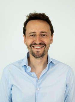
Grünstein, Leo

Grünstein, Leo
CEO
Spiden AG

Grünstein, Leo

Abstract
Today, biomarkers such as urea, lactate, glucose and others are commonly sensed invasively and non-continuously. Spiden's vision is to extend human longevity through its proprietary sensing platform. It allows to measure various biomarkers without the need for fluorescent markers or surface functionalization. This enables real-time and continuous measurements of analytes within patients matching one of the most prevalent medical needs.In this talk, we will describe our recent advances in the field of label-free biomarker sensing.Here, we will discuss our preliminary measurement data of our integrated CMOS spectroscopy detector in comparison to state-of-the-art spectroscopy measurement equipment.An outlook is given about future products using photonic integration and potential routes for the implementation of transcutaneous wearable devices. We will also discuss the current photonic eco system relevant for our applications. In this context we highlight the missing technology platforms, which still hamper the wider spread use of point-of-care and wearable biomedical sensing applications.

Biography
Leo Grünstein is a serial entrepreneur. With his Swiss-based venture builder LG Capital he co-founded 20 ventures from the ground up, raised >600m CHF for them, sold more than half of them successfully (e.g. MoneyPark that was acquired to 70% by Helvetia Insurance for a valuation of CHF 153m in 2017), with the rest either having failed or still being up-and-running. He is the founder and CEO of Spiden, in which Leo found his passion focusing on longevity and health. Spiden is working on the difficult problem of transcutaneous non-invasive sensing of multiple biomarkers. The company built and uses its super-spectral engine + AI to analyse biomarkers and drugs for the first time optically, in-flowing biological fluids (e.g. blood) with the goal to create a unique next-generation wearable device to provide access to unseen biomarker data and help to extend human longevity.Jens Hofrichter, PhD, has 15 years of experience in integrated photonics R&D. He drove the development of the passive components, wafer-level test infrastructure and monolithic laser integration of silicon photonics at IBM contribution to the 100Gbit/s LR4 transceiver. In 2015 he moved to ams, where he was setting up the fully automated optical product validation and optical wafer-level testing capabilities for medical and specialty products. He was in charge of the radiation hard monolithic photodiode development, which led to the development of monolithic computed tomography chips used in 16 and 32 slice CT scanners. He was leading the hybrid bonding development for non-Cu hybrid bonded imaging sensors. After that he was leading the cross-divisional camera team for the development of miniature AR cameras. As co-inventor of the optical microphone, he was appointed program manager of the related industrialization program in the ams-Osram group. In 2022 he moved to Spiden, where he is currently leading the optical and photonic integration activities for next-gen medical sensors. He is the (co)author of more than 30 patent families mainly in the field of photonic integration and imaging sensors.

Integrated Photonics
ST Microelectronics ST Microelectronics Theveniau, Raphael
Complete LVS verification methodology and process for complex System-In-Package assemblies
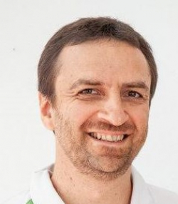
Theveniau, Raphael

Theveniau, Raphael
CAD Support Senior Staff Engineer
ST Microelectronics

Theveniau, Raphael

Abstract
Systems in Package (SiP) have been around for some years and were typically the integration of multiple bare unpackaged chips along with discrete devices interconnected with just a few signals. However, as silicon scaling (aka Moore’s Law) slows and silicon densities reach their physical limits, there is growing shift to disaggregation of once monolithic functions into smaller, node optimized high yield chiplets, heterogeneously integrated on a high-performance substrate as an advanced System-In-Package (SiP), or module. These designs utilize multiple high performance and high bandwidth interfaces between the chiplets enabling higher densities, greater device functionality, and improved overall silicon yield. All the devices used in a SiP are often designed concurrently, by different teams, in different time zones. Thus, the risk to make mistakes in data exchange is very high. To mitigate this risk a comprehensive system description along with a controlled data exchange flow is key. Furthermore, although each device is tested independently, there is a need for a formal signoff check or verification that covers the whole system.In STMicroelectronics we have developed an automated layout versus schematic (LVS) methodology that electrically verifies the module and system-level designs logical connectivity. Using a combined 3D assembly level DRC/LVS methodology our divisions can prevent System in Package failures due to swapped balls, shorted power nets or any uncontrolled change in the design layouts.This paper will describe the essential steps and process of a fully integrated workflow that can verify and validate a complete multi-chiplet SiP design assembly using an LVS approach including the technologies used to enable such a solution.

Biography
After 5 years spent in Cadence UK and 5 years in Texas Instruments France, Raphael Theveniau joined STMicroelectronics in 2009 as System in Package expert. He is now part of Technology R&D group in ST, in Digital Design Flows and Methodology team. He has more than 20 years of experience in Digital Design, covering most aspects of place and route and signoff flows and package design. His role as SiP expert consists in developing, promoting and supporting flows through ST kits for internal divisions as as well as external customers. Now his role is more focused on Die-Package Co-design flows, and more specifically System in Package LVS.

Advanced Packaging Conference
STMicroelectronics STMicroelectronics Champseix, Jean-Louis
Wellbeing and Diversity and Inclusion
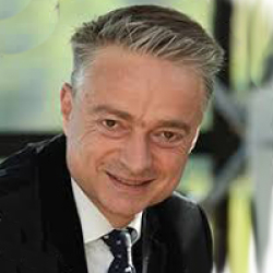
Champseix, Jean-Louis

Champseix, Jean-Louis
Group VP, Head of Sustainability, Learning & Development
STMicroelectronics

Champseix, Jean-Louis

Abstract
Coming Soon

Biography
Jean-Louis Champseix is Group VP, Head of Sustainability, Learning & Development at ST Microelectronics since January 2017. He joined the company in 1992 with the role of Corporate Employment Director. He then became Asia HR Director in 2004 and was appointed as Senior Vice President Head of Human Resources at ST Ericsson from 2008 to 2013. He became Group Vice President, Head of Learning & Development, Social Responsibility, HR Management Systems in September 2013.

Fab Management Forum
STMicroelectronics STMicroelectronics Alba, Simone
Opening Remarks
Alba, Simone

Alba, Simone
AG300 Fab - CVD and Dry Etch Area Manager
STMicroelectronics

Alba, Simone

Abstract
Not available

Biography
Simone Alba has more than 25 years of experience in the semiconductor industry. He got his master’s degree in Physics with specialization in Plasma Physics at University of Milan. After few years spent in the field of plasmas for space applications, he joined STMicroelectronics at Agrate Brianza site (Italy). Holding various managerial roles, he had the opportunity to develop a wide technical experience in technology nodes (350-32nm), technology devices (Flash Memories, Phase Change Memories, Embedded Memories, BCD, …), manufacturing environments (from early R&D to high volume manufacturing). He also had the chance to deal with different company cultures and businesses thanks to strategic projects, technology transfers, benchmark, etc. At present he is CVD/dry etch area manager in the new 300 mm fab in Agrate.

Fab Management Forum
Stockholm Environment Institute Stockholm Environment Institute Michalopoulou, Eleni
Beyond ESG: How can we Maximise the Impact of our Actions Using Integrated Approaches to Enhance and Amplify Action to Achieve the Sustainable Development Goals
Michalopoulou, Eleni

Michalopoulou, Eleni
Research Associate
Stockholm Environment Institute

Michalopoulou, Eleni

Abstract
Coming Soon

Biography
Dr Eleni Michalopoulou joined Stockholm Environment Institute’s York Centre in 2020 as a member of the Air Pollution group where she contributes to Climate and Clean Air Coalition (CCAC) projects and the Supporting National Action and Planning (SNAP) on Short-Lived Climate Pollutants (SLCPs) initiative. She is a member of the World Economic Forum's Global Future Council on Clean Air and she is working with the Alliance for Clean Air on quantifying air pollutant emissions in value chains. She is a co-author in the IPCC’s 2019 Refinement to the 2006 IPCC Guidelines for National Greenhouse Gas Inventories working closely with the aluminium, semiconductor and gas abatement industries. Eleni completed her undergraduate studies in the National and Kapodistrian University of Athens where she received a degree on Physics with a major on Environment, Meteorology and Oceanography. In 2019, she completed her PhD on ‘Quantifying perfluorocarbon emissions using bottom-up and top-down methods’ with the Department of Chemistry of the University of Bristol.

Smart and Green Manufacturing Summit
Summa Semiconductor Oy Summa Semiconductor Oy Helle, Meri
Transition from the Chip and Talent Shortages to Shaping the Next Generation Skills & Talent Building
Helle, Meri

Helle, Meri
CEO & Co-founder
Summa Semiconductor Oy

Helle, Meri

Abstract
Coming soon

Biography
Dr. Meri Helle is the CEO and Co-founder of Summa Semiconductor Oy.Summa Semiconductor is a fully independent company providing semiconductor manufacturing services with the focus on specialized semiconductor devices tailored to customer needs – bridging the gap from prototyping to microelectronics and photonics manufacturing – providing a full pathway from R&D, prototyping and pilot production to high-volume manufacturing. Summa is an active partner in the microelectronics ecosystem and support our customers to find the right partners and talent to meet their needs.Summa is also partner in Erasmus+ METIS consortium 2019-2023 - MicroElectronics Training Industry and Skills – https://www.metis4skills.eu/METIS is bridging the skills gap in the microelectronics sector for a more competitive Europe. The Sector Skills Alliance, co-funded by the Erasmus+ Programme, brings together a consortium of 19 key partners to develop skills intelligence deliver the METIS curriculum and training and promote microelectronics as a career choice.Before founding Summa, Dr. Helle worked for silicon wafer manufacturing company Okmetic. At Okmetic she held a Process Engineer position (2011-2012) at Okmetic’s silicon wafer manufacturing fab in Finland and 2012-2015 she held a Technical Customer Support Engineer position at Okmetic’s sales team with main responsibilities in Taiwan, Singapore and Malaysia. Prior joining Okmetic, Dr. Helle was also part of Nokia Research Center’s graphene research team (2010-2011).After finishing MSc (2001) and PhD (2006) in quantum physics in Aalto University, Finland, Ms. Helle continued her academic career in Low Temperature Laboratory, Aalto University as Academy of Finland Post-Doctoral Researcher Scientist (2006-2010). Her research consisted of superconducting nano electronics device fabrication in the Micronova cleanrooms and cryogenic-temperature measurements of quantum phenomena in superconducting nano-devices.Selected publications:Electronic refrigeration at the quantum limit, Physical Review Letters 102, 200801 (2009). http://prl.aps.org/abstract/PRL/v102/i20/e200801Strong gate coupling of high-Q nanomechanical resonators, Nano Letters 10, 4884 (2010).http://dx.doi.org/10.1021/nl102771pGraphene for future electronics, Proceedings of the Nobel Symposium on Graphene and Quantum Matter, Physica Scripta, Volume 2012, T146. Published 31 January 2012 • 2012 The Royal Swedish Academy of Sciences.https://iopscience.iop.org/article/10.1088/0031-8949/2012/T146/014025/meta

The Future of Work
SUSS MicroTec Netherlands B.V. SUSS MicroTec Netherlands B.V. Hermans, J.P.
Inkjet Printing for Semiconductor Applications

Hermans, J.P.

Hermans, J.P.
Manager Applications
SUSS MicroTec Netherlands B.V.

Hermans, J.P.

Abstract
Inkjet printing is gaining commercial interest, as a sustainable replacement of traditional process equipment in the semiconductor market. Unique features, such as local material deposition with variable thickness, digital processing and virtually zero waste enable the customers reduction to reduce the process complexity and a significant cost saving. In this talk we will present user cases showing the advantages of inkjet printing of photoresist, imprint resist, dielectric materials such as SU-8, polyimide and solder mask compared to traditional process techniques such as screen-print and spin-coating.

Biography
Joost Hermans obtained is M.Sc. degree in Applied Physics at the Eindhoven University of Technology, afterwards he as a process engineer for various companies and from April 2020 at SUSS MicroTec Netherlands B.V, the inkjet department of SUSS MicroTec. Since July 2022 he is working as the manager applications with a primary interest on developing inkjet solutions.

Materials Innovation
SYSTEMA SYSTEMA Roßbach, Philipp
How to Simplify Engineers’ life in Complex Semiconductor Manufacturing - About Democratization of Information and its Usage in Production Scheduling and Root Cause Analysis
Roßbach, Philipp

Roßbach, Philipp
Analytics Solution Engineer EIA
SYSTEMA

Roßbach, Philipp

Abstract
Digitalization keeps driving increased demand for microchips. Shortening the product lifecycle and the high variety of customer-specific devices lead to a growing need for high-mix low-volume (HMLV) semiconductor production. SYSTEMA drives several activities to achieve a novel quality in production control and explainability of how the fab behaves. The “Autonomous Integrated Scheduling for Semiconductor Industry” (AISSI) project partners with Bosch, Nexperia, Simlab, KIT. Goal is to apply AI-based methods to enable autonomous production scheduling. However, such AI-solutions are “black boxes”. They will only be accepted, if users understand the system: “explainability”– see also the EU "General Data Protection Regulation GDPR".Objective is simplifying engineer’s work and hand-over a powerful framework for continuous and rapid learning - and maybe creatig a smile.SYSTEMA created a semantically inspired holistic information model (HIM). This offers, for the first time, an easily understandable access and method to close the gap between huge amount of data and the need to analyze this data in real-time, while offering at the same time the possibility to create formerly unseen, personalized “insights”. The solution concept implements a single point of truth (SPOT) approach, enabling best algorithmic efficiency at the same time. Complex WHAT-IF-Analysis is enabled:- What are the root causes of those dynamically appearing “WIP bubbles”- Did the efficiency of the entire production line sustainably improved when the new scheduling method was introduced?Additionally, counter-factual analysis is enabled – which is critical to enable human learning. The aim is to create an informational 'play space' that is fundamental to human imagination.AI-based methodologies seem to provide important capabilities in order to solve the complex planning task of production or the "job scheduling problem". SYSTEMA has analyzed the requirements together with Nexperia and created a new AI-based scheduling concept utilizing 4M-methodology. Detailed analysis accomplished are, e.g., setup- and occupancy planning of batching machines (furnaces), maintenance and shift activities and many others.Examples highlighted during poster session and presentation will touch a “counterfactual” improvement of an entire production area (such as furnace) and showing its influence on the entire fab;a dive-in into an integrated AI-based scheduling method.

Biography
Philipp Roßbach (Speaker)holds a M.Sc. in Applied Informatics – Data Science from HTW Dresden, University Applied Science (Germany). He started in 2015 at SYSTEMA for his B.Sc., and later during his M.Sc., and supported his first projects for semiconductor manufacturing. Currently, he is 1) contributing to the R&D program AISSI at SYSTEMA while 2) also researching at HTW for Cell-based analysis in systems medicine.For AISSI, (“Autonomous Integrated Scheduling for Semiconductor Industry”) Philipp helps to develop, integrate and apply novel AI-based approaches in semiconductor manufacturing that builds on European quality-thinking from the automotive sector.For HTW, his fields of research are data-driven modeling for the analysis of multicellular tissue organization and model-based prediction of an Effective Adhesion Parameter guiding multi-type cell segregation.Dr. Gerhard Luhn (Mentor)holds a Ph.D in engineering science from the University of Erlangen-Nuremberg (Germany). He has more than 25 years of experience in semiconductor manufacturing and information science. Currently, he is heading an innovation program at SYSTEMA GmbH together with the Technical University of Dresden and several major renowned industry partners, which aims at the industrial proof, prototypical and scientific validation of a new, mathematically grounded method of causal-holistic information processing. Gerhard previously worked as team leader / program manager and research fellow for Infineon/Dresden, Technical University Dresden and Siemens/Munich. He also held various positions in France with Siemens / IBM joint venture in Essonnes; and ST Microelectronics in Crolles. Gerhard holds a patent application, authors scientific papers, and engages in the science of information.

Fab Management Forum
T To top
TECHCET TECHCET Shon-Roy, Lita
Semiconductor Market Expansion Driving Materials Innovation – Materials Market Outlook and Challenge
Shon-Roy, Lita

Shon-Roy, Lita
President/CEO and Founder
TECHCET

Shon-Roy, Lita

Abstract
Coming Soon

Biography
Lita Shon-Roy - President/CEO and Founder of TECHCET— has worked throughout the semiconductor supply chain at various levels leading strategy, business development, marketing and sales for chip designers, equipment OEMs, and electronics material suppliers for over 30 years. Her experience spans from process development of SRAMs to business development of gases & precursors. She developed new business opportunities for companies such as RASIRC/Matheson Gases, Air Products & Chemicals, and IPEC/Speedfam, and managed marketing and sales in companies such as Air Products/Schumacher, Brooktree/Rockwell, and Hughes Aircraft. Ms. Shon-Roy is considered one of the leading experts in electronic materials market research analysis and business development. She has authored and co-authored 100’s of articles, reports and texts on semiconductor process materials markets, trends, and worldwide supply chain issues. She holds an M.B.A. from California State University, Dominguez Hills, a M.S.E.E. focused on Solid State Physics from the University of Southern California, and a B.S. in Chemical Engineering from UC San Diego.

Materials Innovation
TechInsights Inc. TechInsights Inc. Hutcheson, Dan
Frontier of Challenge and Opportunity: Semiconductor Shortages, Geopolitics, & Outlooks
Hutcheson, Dan

Hutcheson, Dan
Vice Chair
TechInsights Inc.

Hutcheson, Dan

Abstract
2020 was a pivotal year in world history that brought unprecedented challenges and opportunities. COVID threw a curveball at the semiconductor industry: decoupling it from the economic cycle, elevating the perception of its importance to economy in the minds of world leaders, as it rang the death knell for globalization. This presentation examines how COVID lead to the Great Semiconductor Shortage of 2021, as business leaders reacted to 2020’s early events in ways that left them unprepared to deal with what came after. There would be an unprecedented rise in demand as the human toll of the virus came to a close only to be left with a ravaged supply chain that could not adequately respond to this demand. It lays out how this unraveled the auto industry’s ability to produce cars as it coped with a shortage of critical chips. Like dominos, COVID tipped the block to knock into the Great Chip Shortage in 2021, which then tipped to knock globalization down. The geopolitics driving a perceived need for national technology sovereignty is examined as it delves into how it started in China in the mid-2010s and was locked in with the Taiwan hyper-coherence issue of the early 2020s.

Biography
Dan is Vice Chair of TechInsights Inc. He is a recognized authority on the semiconductor industry, winning SEMI’s Sales and Marketing Excellence Award<sup>[1]</sup> in 2012 for “empowering executives with tremendous strategic and tactical marketing value" through his e-letter, The Chip Insider®; his book Maxims of Hi-Tech, and his many interviews of executives. As some industry leaders have said, “He is the marketing voice and expert for the industry.” “Dan has methodically captured the essence of the industry and produced it in such a way for all to benefit … He has been such an integral part of the industry for so long, it is difficult to imagine the industry without his contributions.” Dan’s public work on the industry has often focused on challenging predictions of the demise of Moore’s Law that date back decades by demonstrating how doomsayers have been outpaced by emergent behavior through the innate ability of technologists to innovate. This has included invited articles for Scientific American, the SIA, and the Plenary at the SPIE Advanced Lithography Conference.[1] Formerly SEMI’s Bob Graham Award

Fab Management Forum
Technical University of Applied Sciences Regensburg Ramsauer, Ralf
Jailhouse: Mixed Criticality Systems for Semicondutor Manufacturing

Ramsauer, Ralf
Head of Research Group
Technical University of Applied Sciences Regensburg

Abstract
The advent of multi-core CPUs in nearly all embedded markets has prompted an architectural trend towards combining safety critical and uncritical software on single hardware units. We present an architecture for mixed-criticality systems based on Linux that allows for the consolidation critical and uncritical parts onto a single hardware unit. In the context of the iDev 4.0 project, the use-case of this technological building block is to reduce the overall amount of distributed computational hardware components accross semiconductor assembly lines in fabs. CPU virtualisation extensions enable strict and static partitioning of hardware by direct assignment of resources, which allows us to boot additional operating systems or bare metal applications running aside Linux. The hypervisor Jailhouse is at the core of the architecture and ensures that the resulting domains may serve workloads of different criticality and can not interfere in an unintended way. This retains Linux's feature-richness in uncritical parts, while frugal safety and real-time critical applications execute in isolated domains. Architectural simplicity is a central aspect of our approach and a precondition for reliable implementability and successful certification. In this work, we present our envisioned base system architecture, and elaborate implications on the transition from existing legacy systems to a consolidated environment.

Biography
Ralf Ramsauer is a postdoctoral researcher at the Technical University of Applied Sciences Regensburg where he leads the Systems Architecture Research Group. His academic research interest focuses on mixed- and safety-critical systems, real-time embedded systems and embedded virtualisation on various architectures. This covers the full software stack of embedded systems, from hardware-related low-level virtualisation technologies via kernel-space up to userland. Ralf is a codeveloper of the Linux-based statically partitioning hypervisor Jailhouse, where he currently works on the RISC-V port.

Fab Management Forum
Technical University of Sofia Technical University of Sofia Malenkova, Slava
ECoVEM European Centre of Vocational Excellence in Microelectronics
Malenkova, Slava

Malenkova, Slava
Researcher
Technical University of Sofia

Malenkova, Slava

Abstract
The ECoVEM project brings together VET centres, polytechnics, industrial associations, and social partners into a European cooperation platform of vocational excellence in microelectronics to tackle the challenges in upskilling and reskilling, sustainable development, digitalisation and resilience. ECoVEM builds on and complements the strengths of national VET systems in countries with more-advanced VET and supports the not so advanced regions to achieve VET excellence. ECoVEM implements innovative instructional approaches towards life-long capacity to self-regulate learning, hard skills and soft skills using the ecosystems-based theoretical models and performance support systems. ECoVEM sets up und implements an action plan for business-science-education cooperation, as well as an action plan for collaboration for effective governance in the microelectronics sector.

Biography
Slava Malenkova works as researcher and project manager at TU Sofia. She has a background of international education with a PhD in quantum physics from Austria, MSc in physics from Germany, and a dual French-German highschool education from France.

The Future of Work
TERADYNE TERADYNE Ducrocq, David
Minimizing Execution Risk in Test Solution Development Projects with a Technical Project Lead
Ducrocq, David

Ducrocq, David
Application Test Technical Leader
TERADYNE

Ducrocq, David

Abstract
Test development projects are a mix of engineering disciplines spanning PCB design and layout, software engineering, measurement technology, test system configuration and test cell setup, a complex and interdependent ecosystem. A project manager, who is primarily focused on schedule, is unable to oversee the many disciplines and adequately assess technical risks in each area and across the entire project. This inability to assess risks and their impact on the entire project is often the root cause of catastrophic project failures and missed delivery schedules. By including a technical project lead in the project, there is a single point of responsibility for assessing technical risk across the project, developing mitigation plans and driving countermeasures to completion.This paper will address:1. The role the technical project lead plays with each stakeholder in the project and to the project as a whole, including:1.1 solution architecture1.2 resource identification and allocation1.3 technical execution of the project1.4 issue mitigation and resolution1.5 communications with both internal and external stakeholders2. Qualifications of a technical project lead3. An overview of the risk assessment and mitigation process4. Expected benefits to the project, team and working environment

Biography
David Ducrocq is an Application Project Leader at Teradyne, where he focuses on PMIC and Image Sensor Test program development and is a specialist on Teradyne’s FLEX, MicroFLEX and UltraFLEX test systems. David has played a leading role in defining and implementing Teradyne’s technical project lead program across the organization. David joined Teradyne in 1999 as an Applications Engineer for the Test Assistance Group in Grenoble/France, where he worked on Catalyst on RF Devices.David studied Electrical Engineering and Computer Science at the Institute de Recherche et d'Enseignement Superieur aux Techniques de l'Electronique* (IRESTE), Université´ de Nantes, France.After graduation, David worked in the field of Image Processing for 2 years. He then worked as a subcontractor for Teradyne for 4 years on the A3xx, A5xx and Catalyst test systems.In 1999, David joined the Test Assistance Group at Teradyne in Grenoble/France as an Applications Engineer. David worked on Catalyst on RF Devices and is now a specialist on FLEX/MicroFlex/UltraFlex test systems.From 2012, David took the responsibility of several key customers as an Application Project Leader mainly focusing on PMIC and Image Sensor Test program development. During this period, David played a leading role in definition and implementation of the technical project lead and was in charge of its roll-out throughout the corporation.*Institute of Research and Higher Education for the Techniques of Electronics

Innovation Showcase
Texas Instruments Texas Instruments Schimpf, Klaus
Not available
Schimpf, Klaus

Schimpf, Klaus
Fab Manager
Texas Instruments

Schimpf, Klaus

Abstract
Not available

Biography
now 25 years with TI- 1997: Phd in Physics Research Centre Juelich- 1997: joining TI in Freising as Product engineer working on Development and yield improvement of Annalog technologies- 2007-2020: various mgmt roles in Engineering and Operations- 2021: Fab Manager , FFAB TI Freising

Fab Management Forum
Texas Instruments Texas Instruments Thomas, Vipin Koshy
Machine Learning for Automated Image Classification in Yield Enhancement
Thomas, Vipin Koshy

Thomas, Vipin Koshy
Intern
Texas Instruments

Thomas, Vipin Koshy

Abstract
One of the most repetitive and time-consuming tasks for our operation specialists in the Yield Enhancement group is the manual image classification. Moreover, due to stress and environmental conditions the consistency and accuracy of the manual classification varies. Therefore, we have been looking for a fully automated solution to relieve our specialists from the tedious classification tasks. In addition, the implementation of the solution to our production flow and integration to our fab automation has a positive impact on productivity.We have explored various options available for out pilot automated classification project and found Convolutional Neural Networks (CNN) can produce consistent and accurate results for one specific classification task. We use a generally accepted CNN classification model trained on thousands of images from the scanning electron microscope. Since the input image dataset was highly biased, we used Image augmentation techniques to improve the results. In addition, we have also considered techniques like Transfer Learning to scale our solution to other image classification tasks. Our current model outperforms in terms of consistency and accuracy when compared to the manual classification.We will achieve more by integrating fab automation to the automated image classification. A successful completion of the classification tasks triggers the fab automation to check whether to logout the lot, to inspect more wafer from the same lot or to put the lot on hold. With a fully automated fab process, we can minimize delays and waiting times of wafers. So far, we have been successful in implementing and integrating automated image classification with fab automation as a pilot project. We have identified a high fan out potential of this automated classification method and will be working to transfer the promising results to other areas as well.

Biography
Vipin holds a bachelor degree in Computer Science and Engineering from Mahatma Gandhi University, India (2013). He has worked for about 4 years in various companies (2014 - 2019) and gained knowledge on diverse technologies and frameworks such as mainframes, angular framework, data analysis with Python, cloud and Data Science/ML frameworks. Since Oct 2020, he is pursuing a MSc. Applied Computer Science at TH Deggendorf with expected graduation in Apr 2023. Currently, he is working at Texas Instruments as an Intern (Mar 2022 - Aug 2022). He is interested in Data Science projects and Edge AI.

Fab Management Forum
time:matters GmbH time:matters GmbH Kohnen, Alexander
Panel Discussion – Navigating through global developments affecting the supply chain management
Kohnen, Alexander

Kohnen, Alexander
CEO
time:matters GmbH

Kohnen, Alexander

Abstract
10:30 - Panel Discussion – Navigating through global developments affecting the supply chain management How can we enable improvements in supply chain?Supply chain changes / access to x (materials, tools, etc e.g. lead time to tools) / Supply chain management post covid / new relationships / how can we help our suppliers to faster deliveryhow to scale material supply/capacity exponentiallyGlobal development on supply-customer relationship based on covid-era lessons learntTool usage beyond expectancy (legacy tools) in fabs, what will it happen in these technologies in a few years (sustainability aspect)? Moderator: Dan Hutchinson, CEO and Chairman, VLSI

Biography
Alexander Kohnen is CEO and Managing Director Strategy and Sales for time:matters Holding GmbH in Neu-Isenburg. As an expert in high-performance and worldwide special speed logistics and in time-critical international spare parts logistics, time:matters provides tailor-made and fast solutions for particularly urgent and complex logistical tasks. Besides speed and reliability, providing an individual, flexible service is paramount.Alexander Kohnen began his career in 2000 as Information Manager Sales & Marketing with Lufthansa Cargo AG in Frankfurt am Main. In his 17 years with Lufthansa Cargo, he gained extensive management experience in various leadership roles at home and abroad, including a period from 2008 as Country Manager Sales and Handling Benelux in Amsterdam. He moved to Stockholm in 2011 to take up the role of Director Sales and Handling Nordics & Baltics, covering sales, marketing and commercial management in Scandinavia. Before his switch to time:matters, he was most recently Senior Director with responsibility for the Industry Development & Product Management division at Lufthansa Cargo in Frankfurt.In November 2017, Alexander Kohnen joined the management team at time:matters. The company finished that same year with a 55% year-on-year increase in revenue and registered tremendous growth in the automotive and high-tech/semicon focus industries. Under Alexander Kohnen’s leadership, time:matters has added another 17 stations (Tel Aviv, Mexico and 15 stations in the US) to its unique Sameday Air network for same-day transports. The logistics company has also been awarded ISO 14001:2015 environmental management certification. By acquiring CB Customs Broker and Customs Broker Cargo Handling, time:matters has been able to extensively expand its customs clearance and handling portfolio. In the coming year, with Alexander Kohnen at its helm, the company is again planning countless internationalization projects, further digitization of its offering, connection of customer and partner systems via APIs and further development of its time:matters airmates On Board Courier platform.time:matters is now considered one of the leading providers of flexible special speed solutions. The internationally renowned logistics specialist has already been operating extremely successfully in the sector since 2002, which has been continuously reflected in its positive revenue trend. In 2017 time:matters concluded with 108 million euros in revenue.The native of Cologne trained as a commercial air transport apprentice with Lufthansa AG in Frankfurt, before going on to complete a Business Administration degree. Alexander Kohnen is married and has three children.

Fab Management Forum
Trinity College Dublin Boland, John
Nanoscale Metals are Comprised of Grain Boundaries that are Significantly Different from those found in Bulk Materials
Boland, John

Boland, John
Professor of Chemistry
Trinity College Dublin

Abstract
Metals are the simplest of solids and copper is probably the best known and most studied of all. The properties of copper metal of macroscopic dimension are well understood. However, the same cannot said when copper is reduced to nanoscale dimensions. Like most metals, copper is a granular solid comprised of grains with boundaries between them. Here in this talk we focus on what we have learned about nanoscale copper by using scanning tunneling microscopy and molecular static simulations. In particular we visualize for the first time the 3D structure of grain boundaries (GBs) that emerge at the surface of nearly coplanar copper nanocrystalline (111) films. Remarkably, we find that GBs at surfaces are different from those in the bulk. We show that GBs in metals actually prefer to lie along close packed planes which in turn necessitates the tilting and restructuring of the boundary as it approaches the (111) surface. The restructuring depth can be a few to several tens of nanometers. This behavior is due to a previously unrecognized phenomenon that involves the rotation of the dislocation lines that comprise the GB, which minimize the energy and has significant implications for materials properties [1, 2]. Since transport in copper occurs predominantly along close packed planes these restructure boundaries, which also lie along close packed planes, are expected to have unusual scattering properties. Whether fully relaxed restructured boundaries are possible under device fabrication conditions remains to be established.References:[1] Xiaopu Zhang, Jian Han, Adrian P. Sutton, David J. Srolovitz, John J. Boland. Science 357, 397-400 (2017)[2] Xiaopu Zhang, Hailong Wang, Moneesch Upmanyu, John J. Boland (under review)

Biography
Prof John Boland received a BSc degree in chemistry from University College Dublin and a PhD in chemical physics from the California Institute of Technology, where he was an IBM graduate fellow and recipient of the Newby-McKoy graduate research award. From 1984 to 1994 Prof Boland was a member of the research staff at the IBM T.J. Watson Research Center (New York). In 1994 he joined the chemistry faculty at the University of North Carolina at Chapel Hill where he was appointed the J.J. Hermans Chair Professor of Chemistry and Applied and Materials Science. In 2002 Prof Boland moved to the School of Chemistry at Trinity College Dublin as a Science Foundation Ireland Principal Investigator and Professor of Chemistry. In June 2005 he was appointed Director of the Centre for Research on Adaptive Nanostructures and Nanodevices (CRANN) until July 2013. He also served as TCD Vice President and Dean of Research (2015-2017).Prof. Boland became an elected Fellow of Trinity College Dublin in 2008, a fellow of the American Vacuum Society (AVS) in 2009 and a fellow of the American Association for the Advancement of Science (AAAS) in 2010. He was the 2011 laureate of the ACSIN prize for nanoscience. He is the recipient of an Outstanding Researcher Awards from IBM (1992) and Intel (2017). He is the recipient of a prestigious European Research Council Advanced Grant. Prof. Boland’s research interests are focussed on the novel properties of nanoscale materials and their potential in device and sensor applications.

Materials Innovation
TU Dublin TU Dublin Kelleher, John
Green AI
Kelleher, John

Kelleher, John
Professor
TU Dublin

Kelleher, John

Abstract
Coming Soon

Biography
John’s core research expertise is in the areas machine/deep learning and natural language processing. He is the TU Dublin lead in the ADAPT centre and the scientific lead for the Digital Content Transformation Strand. Within the ADAPT centre he leads research projects on language modelling, lexical semantics, machine translation, novelty detection, image captioning, dialog systems, and making AI more environmentally sustainable. John has been the academic lead on numerous industry projects across a range of topics and domains, including: anomaly detection, transfer learning, customer segmentation and propensity modelling, dialog systems and chat bots, and information retrieval and natural language processing.

Smart and Green Manufacturing Summit
Tyndall National Institute Tyndall National Institute Ghosh, Samir
Heterogeneously Integrated InP-laser on Silicon Photonics realized by Micro-Transfer Printing
Ghosh, Samir

Ghosh, Samir
Researcher
Tyndall National Institute

Ghosh, Samir

Abstract
Silicon photonics have gained immense commercial interest in data-center market and soon it will enter other domains as well including biomedical, space applications and so on. Silicon being an indirect bandgap semiconductor efficient lasing cannot be achieved. Therefore, hybrid or heterogeneous integration techniques are normally used to incorporate laser with silicon photonics (SiP) platform. These techniques of integrating lasers on SiP platform are far from ideal in-terms of volume, cost and yield. Micro-transfer printing is an emerging technology which enables massively parallel integration with high yield and hence bring the cost down. In this talk transfer printing of InP-based laser on SiP chip will be presented.

Biography
Samir Ghosh obtained his Ph.D. degree in Photonics Engineering from Ghent University, Gent, Belgium in 2013. Afterwards he worked at various academic institutes as a postdoctoral researcher including McGill University – Canada, University of California - Davis, The University of Tokyo - Japan, and Nanyang Technological University - Singapore. Since October, 2020 he is working as a researcher at Tyndall National Institute, Cork, Ireland where his primary interest lies on heterogeneous integration of InP, LN-based devices on Si-Photonics platform utilizing micro-transfer printing technology. His has (co-) authored of 30 publications in referred journals and in international conference proceedings. His broad research interests include large-scale photonic integrated circuit for communication, sensing and imaging applications.

Integrated Photonics
V To top
Volkswagen Volkswagen Aal, Andreas
Joint Risk Management Paves the Way to Sustainable Supply Chains & Innovation
Aal, Andreas

Aal, Andreas
Semiconductor Strategy & Reliability
Volkswagen

Aal, Andreas

Abstract
The necessary automotive transformation creates challenges and opportunities that cannot be addressed by only setting ecological targets. It is mandatory to set up a plan under given and dynamically changing economical and geo-strategical constraints. Since the beginning of the pandemic and its supply shortage after-wave combined with previously not sufficiently risk assessed geo-strategical “impacts”, we all have lessons learned while part allocation task forces running day-by-day in parallel occupying a lot of resources and costs in addition to shortage originating not sold goods. This situation creates a lot of uncertainty about which directions to take and decisions / investments to make (risk function) along the supply chain, because company internal risk management processes remain internal while information from the “outside” world (input signal) is biased (not sufficiently aligned). This is all coming on top of transformation created supply challenges in the automotive industry like battery efficiency being depended on needed raw materials in a global supply chain, limited manufacturing capacity for power electronics whose capacity increase is slowed down by the semiconductor shortage affecting fabrication tool availability plus the not yet achieved electronic architecture switch away from uncountable ECU variant implementations. While cyber security is considered as “the” challenge of the electronics industry for the running decade, supply related root-of-trust processes will become even more mandatory – however, current risk management approaches are limited and supply issues will tend to last … until new collaboration models are jointly build, agreed and running.

Biography
Andreas (IEEE SM / CRP) drove the semiconductor strategy & reliability assurance activities within the E/E development at Volkswagen, Germany, for many years, concentrating on technology capability enhancement of most advanced nodes incl. improved HW integration schemes as well as optimization of power electronics for automotive applications. He temporarily joint CARIAD SE between 2020 and 2022 as system architect and product security officer with focus on semiconductor and SW driven innovations. Wearing always one shoe from the semiconductor industry and the other one from the car OEM, he became a strong representative of the through-the-supply-chain-joint-development and collaboration approach also being rewarded with the EDA Achievement award 2020. He has 24 years of experience with and within the semiconductor industry, has authored/co-authored over 40 publications on reliability and has given tutorials at IEEE IRPS and IIRW as well as invited and keynote speeches during various conferences and conventions. His early collaboration activities began already in 2007 becoming the chair of the German VDE ITG group MN 5.6 on (f)WLR, reliability simulations and qualification. He is currently also chair of the European chapter of the SEMI Global Automotive Advisory Council (GAAC), member of the coordination team of the corresponding “European platform for automotive semiconductor requirements along the supply chain” hosted by the VDE ITG and member of the Bmbf industry advisory board on cyber security. Driving the disruptive automotive transformation process on a collaborative supply chain basis is one of his major passions.

Fab Management Forum
W To top
Wooptix Wooptix Gaudestad, Jan
New Metrology Technique for Measuring Patterned Wafer Geometry on a full 300mm wafer
Gaudestad, Jan

Gaudestad, Jan
VP Business Development
Wooptix

Gaudestad, Jan

Abstract
The flatness of the silicon wafers used to manufacture integrated circuits (IC) is controlled to tight tolerances to help ensure that the full wafer is sufficiently flat for lithographic processing. Chemical-Mechanical Planarization (CMP) is one of many processes outside the lithographic sector that will influence wafer flatness across each image lithographic exposure section field and across the wafer. Advanced lithographic patterning processes require a detailed map of the wafer shape to avoid overlay errors caused by depth-of-focus issues. In recent years, a metrology tool named PWG5TM (Patterned Wafer Geometry, 5th generation), based on using double Fizeau interferometry to generate phase changes from the interferometric pattern applied to the reflective surface, has been used to generate a wafer geometry map to correct for process induced focus issues as well as overlay problems. In this paper we present Wave Front Phase Imaging (WFPI); a new patterned wafer geometry technique that measures the wave front phase utilizing two intensity images of the light reflected off the patterned wafer. We show that the 300mm machine acquires 7.65 million data points in 5 seconds on the full 300mm patterned wafer with a lateral resolution of 96µm. For the semiconductor industry to uphold Moore’s Law, among the key challenges are the ever-tightening overlay requirements. In the latest immersion scanners that perform at the sub-2 nm overlay level, the overlay budget becomes more and more determined by process-induced overlay errors from fab steps such as etching, thin film deposition, Chemical-Mechanical Planarization (CMP) and thermal anneal. All these processing steps can introduce stress, or stress changes, in the thin films on top of the silicon wafers that again can result in significant wafer distortions. Since the data acquisition time of Wave Front Phase Imaging (WPFI) is mainly controlled by the shutter speed of the camera when used in a dual camera set up, which is generally set to less than a second, in addition to very high data count, it makes WPFI a strong alternative technique for measuring and correcting for process induced stress quickly. Adding that WFPI is highly resistant to vibrations in addition to having large tolerances to wafer placements in the optical measurement cavity, makes WFPI a viable solution in a high-volume device manufacturing fab setting.

Biography
Jan Gaudestad is San Francisco based VP of Business Development for Wooptix, a small VC funded Intel Capital portfolio company, that is developing metrology equipment for the semiconductor fab market. He also serves on the board of directors for Elevate Semiconductors, a fables semiconductor company based in San Diego California. He has more than 20 years of experience in the semiconductor industry. He worked on strategic accounts at InvenSense/TDK for consumer level MEMS motion sensors. He spent 14 years at Neocera, an Intel Capital funded backend semiconductor equipment company managing product development, global sales, applications, and new business development. He also spent time working on emerging technologies for virtual and augmented reality applications. He received his MBA from Santa Clara University in 2009. He earned a master’s degree in Physics in 2001 from University of Maryland, College Park, and a master’s degree in Physics in 2000 from the Norwegian University of Science and Technology in Trondheim, Norway.

Innovation Showcase
X To top
X-fab X-fab von Podewils, Mario
Opening Remarks
von Podewils, Mario

von Podewils, Mario
Director MEMS & Erfurt Operations
X-fab

von Podewils, Mario

Abstract
Non applicable

Biography
Mario von Podewils has more than 40 years of experience in microelectronics manufacturing. In 1982, he started his career as a maintenance technician for various types of semiconductor manufacturing equipment in the microelectronics industry in Erfurt, Germany. After obtaining his degree in electronics engineering, he spent several years as a team leader responsible for equipment maintenance in various process areas in wafer fabrication at Thesys GmbH, Erfurt. From 1992 to 2001, he was project manager of national and international joint projects in the semiconductor industry, mainly funded by the BMBF or the EU.In 2001, he obtained his diploma in industrial engineering, specialising in operations and production management. Since then, he has held various positions as department and module manager for equipment engineering and the lithography module at X-FAB Semiconductor Foundries AG, among others. In 2007, he took over the position of Fab Operations Manager at X-FAB Semiconductor Foundries GmbH in Erfurt.At the beginning of 2021, he was delegated to the MEMS site in Itzehoe of the XFAB Group as Site Manager. Since autumn 2022, as Director MEMS & Erfurt Operations, he is now responsible for both wafer fabs at the Erfurt and Itzehoe sites as well as X-FAB's global MEMS production.

Fab Management Forum
X-FAB Dresden X-FAB Dresden Tillner, Rico
How medical devices are changing the customer-foundry relationship
Tillner, Rico

Tillner, Rico
CEO
X-FAB Dresden

Tillner, Rico

Abstract
Over the last years the medical industry was pushing for more automation to improve time to result and cost. The Covid pandemic has given another push in this direction.Automotive driven foundries are the perfect partner for the medical industry as they are used to long qualification times and even longer product lifecycles which are also needed in the medical business. Medical and life science applications also require functionalities which cannot be bought out of the shelf. Designer and foundry partners need to develop a close partnership to create a successful product for these markets.Life science companies like MaxWell Biosystems are designing such unique chips for very dedicated use cases. The CMOS-based microelectrode arrays of MaxWell Biosystems are integrating 26’400 platinum microelectrodes in an array, using a MEMS process. These electrodes are used to pick-up the minute signals of neurons, cultured directly on top of the microelectrode array. Together with the use of induced pluripotent stem cells this enables an unprecedented access to human disease models in a dish for drug discovery in the pharmaceutical industry, increasing the potential success of new medicines for neurodegenerative diseases.X-FAB as pure play foundry has developed unique skills to support customers like MaxWell Biosystems, no matter if they are startup companies or big players in their markets.

Biography
Rico Tillner has 15 years of experience in the semiconductor industry. After his master’s degree in electrical engineering at Technical University Dresden he started his career at X-FAB Dresden. From 2007 until 2015 he worked as Process integration engineer, responsible for a 0.6µm automotive mixed signal technology. During that time, he gathered experience in quality methods, yield improvement projects and the conversion from a 6-inch to an 8-inch production. In 2016 he becomes the quality manager of X-Fab Dresden. Since 2018 Rico Tillner is the site manager and CEO of X-FAB in Dresden. Co-presenter Urs FreyUrs Frey received the diploma in electrical engineering from ETH Zurich, Switzerland, in 2003 and the Ph.D. degree for his work on high-density neural interfaces and microhotplate gas sensors from the Physical Electronics Laboratory, ETH Zurich, in 2008. From 2009 to 2010, he was with IBM Research Zurich, Switzerland, where he worked on mixed-signal circuit design for non-volatile memory devices. In 2011 he joined the RIKEN Quantitative Biology Center in Kobe, Japan, where he was heading an independent laboratory focusing on CMOS-based bioelectronics and biosensors. In 2016, he co-founded MaxWell Biosystems AG in Switzerland, where he is currently the CEO.

Fab Management Forum
X-FAB Group X-FAB Group Schoder, Henryk
The People Challenge: How to Overcome the Skill Shortage in the FAB´s?
Schoder, Henryk

Schoder, Henryk
Vice President Human Resources
X-FAB Group

Schoder, Henryk

Abstract
In the light of Europe’s ambition to reinforce the semiconductor ecosystem in the EU with announcement of the Chips Act and significant planned investments into the semiconductor industry, the key to success has be and will be the ability to attract and keep the people required to run a fab. On the level of technicians we already see a substantial shortage in skills and people, and with the new stimulation package that shortage will become a major obstacle for growth ambition in the industry. The presentation will cover some important initiatives and ideas to tackle the problems particular in the are of Manufacturing.

Biography
Since 2014, Henryk Schoder has been overseeing the global HR activities for the X-FAB Group as VP Human Resources. Prior to joining X-FAB, Henryk was HR & IT Manager at Masdar’s solar manufacturing plant in Germany. Before that he worked as Senior Consultant and Managing director for the MRL Consulting Group in the UK, Singapore and Dubai. He started his career as recruiting manager at Infineon. Henryk holds a Master degree in Psychology from the University of Jena, Germany.

Fab Management Forum
X-FAB Group X-FAB Group U’Ren, Gregory
Industry Talk: Opportunities for Innovation in Integrated Device Technologies

U’Ren, Gregory

U’Ren, Gregory
Director RF Technologies
X-FAB Group

U’Ren, Gregory

Abstract
The evolution of communication standards with additional spectrum including mmW and higher order modulation schemes to improve spectral efficiency require advancements of integrated device technologies for the RFFE on a wide range of RF performance metrics such as linearity, gain, and noise. Incumbent technologies for switching, filtering, and signal amplification in receive and transmit paths have weaknesses particularly for mmW and create opportunities for alternatives. At X-FAB we anticipate a necessary evolution of RFFE technology solutions and are committed to meet these challenges pursuing a strategy of heterogeneous integration at wafer or transistor level. We approach these challenges and new opportunities with a holistic perspective striving to not only create and integrate high performance active devices but also to provide a technology solution complemented with foundational IP and a proven application-based demonstrators to validate the design flow and device technology. A perspective on potential next generation technology solutions will be discussed.

Biography
Dr. Gregory U’Ren is the Director of RF Technologies at X-FAB responsible for incubating and subsequently delivering integrated device technology solutions including reference designs and foundational design IP. During his career, he has held both leadership and individual roles contributing to the advancement of a broad range of specialty technologies including SiGe BiCMOS, RF-SOI, MEMS, and GaN. Current activities are focused on the RF front end for 5G or 6G systems engaging various collaborations with academic and industrial partners on a wide range of topics including materials, process, RF/mmW characterization, advanced modeling, and EDA tooling enhancements to support several program initiatives at X-FAB.He is a senior member of IEEE, a member of the American Physics Society, and holds over 30 patents. He completed his PhD and MS at the University of California Los Angeles.

ITF Beyond 5G
X-FAB Semiconductor Foundries GmbH X-FAB Semiconductor Foundries GmbH Kittler, Gabriel
Panelist
Kittler, Gabriel

Kittler, Gabriel
CEO Site Erfurt
X-FAB Semiconductor Foundries GmbH

Kittler, Gabriel

Abstract
Coming soon

Biography
Gabriel Kittler ist Site CEO of X-FAB in Erfurt (Germany). From 2012 to 2020 he coordinated as Innovation Manager all activities concerning emerging technologies and collaboration with universities, research centers, and industrial partners. In 2007 he started in the Process Development at X-FAB with focus on TCAD simulations for HV devices at different technology nodes. He studied Electrical Engineering with focus on Microelectronics at the Technical University of Ilmenau and holds a Ph.D. in Electrical Engineering and Information Technologies.

Integrated Photonics
X-FAB Silicon Foundries SE X-FAB Silicon Foundries SE Bretthauer, Ulrich
Foundry Solutions for Medical Semiconductor Sensors
Bretthauer, Ulrich

Bretthauer, Ulrich
Product Marketing Manager Medical
X-FAB Silicon Foundries SE

Bretthauer, Ulrich

Abstract
Modern medical devices rely on semiconductor technologies for reliable and accurate operation. The application of integrated sensors that record different physiological parameters is of paramount importance. These sensors usually require adaptation to the specific purpose. This presentation will introduce solutions for life-science applications based on CMOS sensor technologies and their targeted expansion to form microfluidic devices. Application specific adjustments must be made in cooperation with the end customer. The variety of medical applications that can be addressed with these semiconductor sensors is huge and the potential that these hold for future product development is exciting.

Biography
Dr. Ulrich Bretthauer has more than 30 years of experience in the design of analog/mixed-signal integrated circuits for various applications from automotive, industrial and communications.After working on energy-efficient processor technologies in Intel's corporate research group. He joined X-FAB in 2015 as product marketing manager for the medical segment, where he oversees the application of X-FAB’s processes in applications from personal medical devices and medical imaging to Lab-on-a-chip devices.

Smart MedTech