3 To top
3M 3M Grommes, Walther
3M Insulative Thermal Bonding Film (ITBF) for Power Module Packaging
Grommes, Walther

Grommes, Walther
European Application Development
3M

Grommes, Walther

Abstract
Abstract:The traditional substrate used in power modules is ceramic based, and typically called a Direct Bonded Copper (DBC) substrate. Comparing to DBC, the newly emerging Insulated Metal Substrate (IMS) shows benefits in smaller and thinner design with higher power density, better warpage control in packaging processes, and potential overall cost reduction, while offering comparable heat dissipation. The key insulation material in IMS is the organic composite thermally conductive sheet bonding to both copper foil and baseplate. The current challenges for this insulation material is how to improve its thermal conductivity, insulation properties, processability and long term reliability.In this presentation, we introduce a new 3M solution for Insulative Thermal Bonding Film (ITBF) for IMS substrate in power module packaging. Based on 3M thermal management material technologies for filler, polymer and processes, we have developed a thermal bonding film with thermal conductivity up to 12 W/mK, and with superior insulation breakdown voltage >6.5 KV at thicknesses of 120 and 150 μm. Material aging and shelf life studies have been conducted. 3M ITBF film showed stable performance in 3000-hour aging tests at 150oC, showing 3M ITBF advantages in product handling and reliability. IMS substrates have been fabricated with 3M ITBF film and have demonstrated good copper bonding and lamination processability. Both thermal resistance and dielectric insulation have been measured based on industry standard methods, demonstrating that 3M ITBF film can enable high performance IMS. Based on the fabricated IMS substrate, a materials model was established. Simulations of heat dissipation and stress management demonstrated that 3M ITBF can significantly reduce insulator stress and slightly improve chip solder stress. Furthermore, the development of 3M ITBF roadmap is discussed.Walther Grommes, Patricia Tien, Monroe Wang, Davie Wang, Koji Ito, Evelyn Liao, Marc Dunham, Benson Chen, Wei Zou

Biography
Walther Grommes has many years of experience in the semiconductor industries as a manufacturing & process development engineer.Bachelor Professional of Chemical Production and Management, 1996, IHK Munich.Since 2007 at 3M in the Electronics Markets Solutions Division, responsible as European Application Development Specialistfor various semiconductor applications on adhesive & tape solutions, wafer support system for thin wafer solutions, cleaning & coating solutions.

Advanced Packaging Conference
A To top
Airbus Airbus Ombach, Grzegorz
The Future of Aviation

Ombach, Grzegorz
Head of Disruptive R&T, Senior Vice President
Airbus

Ombach, Grzegorz

Abstract
The future of aviation is more electric and more autonomous. Reducing emissions from the transportation sector on the road, sea, and the air is one of the fastest ways to combat climate change.The aviation industry represents approximately 2.5% of global human-induced CO2 emissions. But aviation is not the problem. Emissions are the problem.Airbus, is committed to leading the decarbonisation of the aerospace sector. Airbus's vision is to reach net-zero carbon emissions by 2050. This includes reducing the CO2 emissions of our aircraft, helicopters, satellites and launch vehicles, as well as our industrial environmental footprint at sites worldwide and throughout our supply chain.Today, a zero-emission flight is closer to reality than ever. At Airbus, we are committed to developing, building and testing alternative-propulsion systems – powered by electric, hydrogen and other technologies to enable the aviation industry to disruptively reduce the CO2 emissions of commercial aircraft, helicopters, and future urban air mobility vehicles. We are working to deliver on our ambition to bring the world’s first zero-emission commercial aircraft to market by 2035.Additionally, the more autonomous flight can deliver increased fuel savings, reduce airlines' operating costs, and support pilots in their strategic decision-making and mission management. The various technology bricks help to build certifiable, safe and secure autonomy systems and programmes to power the next generation of commercial aircraft applications.

Biography
Dr Grzegorz (Greg) Ombach,Head of Disruptive R&T, Senior Vice President at AirbusGrzegorz (Greg) is passionate about managing technological innovation from an idea to broad market adoption. His combination of technology, leadership and commercial expertise together with a truly global outlook, having worked across Europe, the USA and China, puts him in a solid position to drive international market success for high-tech innovations.As a Head of Disruptive R&T, he shapes Airbus's ability to be the global leader in innovation and future technologies across all Airbus divisions. He works very closely with all businesses and divisions globally. Before as Executive Vice President, Head of Battery Systems Business and Group Strategy and Innovation at Dräxlmaier, he was responsible for the strategy for the business and led the entire product commercialisation, from the initial concept to high volume production of cutting-edge technology in a premium market for the automotive sector. One example is the first high volume production of an 800V battery system for the Porsche Taycan. Earlier, he worked at Qualcomm as a Global Vice President and General Manager of a breakthrough automotive technology licensing business.He also has experience from Siemens VDO, Continental and Brose.Grzegorz holds a PhD in Electrical Engineering from the Silesian University of Technology, Poland and a Certificate in Global Management from INSEAD, The Business School for the World. He has also been awarded Guest Professorship at the Zhejiang University in China.

Executive Forum
Alemnis AG Alemnis AG Widmer, Remo
Recent innovations in Scanning electron microscope in situ mechanical testing for semiconductor failure analysis
Widmer, Remo

Widmer, Remo
Application Engineer
Alemnis AG

Widmer, Remo

Abstract
With the growing complexity of integrated circuits (IC) comes the issue of quality control during the manufacturing process. In order to avoid late realization of design flaws which could be very expensive, the characterization of the mechanical properties of semiconductor components needs to be carried out in an efficient and standardized manner. The effects of changes in the manufacturing process and materials used on the functioning and reliability of the final device also need to be addressed.Micromechanical tests performed in situ (usually in SEM) are already being used to investigate material properties at very small scales. This talk will introduce the concept and how such techniques can specifically be applied to semiconductor materials and electronics components. Such measurements have moved beyond the basic measurement of hardness and elastic modulus to encompass a host of different mechanical properties such as strain rate sensitivity, stress relaxation, creep, scratch resistance, coating adhesion and fracture toughness by taking advantage of focused ion beam milled geometries. New developments, such as high cycle fatigue, are extending the range of properties which can be studied. Novel piezo-based nanoindentation methods are now allowing access to extremely high strain rates (>104 s-1) and high oscillation frequencies (up to 10 kHz).This talk will focus on recent developments in instrumentation for in-situ semiconductor testing at the micro and nanoscales, with specific focus on a testing platform capable of strain rate testing over the range 0.0001 s-1 up to 10’000 s-1 (8 orders of magnitude) with simultaneous high-speed actuation and sensing capabilities. Recent advances in wafer and device level automated testing, including fast mapping, will also be covered.The additional challenge of performing mechanical testing at true in-service operating conditions (e.g., over the temperature range -150 to 1000 °C) will be discussed together with the associated technological and protocol advances required. The inherent advantages of using small volumes of sample material, e.g., small ion beam milled pillars, will be discussed together with the associated instrumentation, technique development, data analysis methodology and experimental protocols. Some examples of test data will be presented on bonding pads, solder bumps and semiconductor coatings.

Biography
Remo N. Widmer holds a B.Sc and M.Sc in Earth Sciences from University of Bern (CH) and a Ph.D. in Material Sciences from University of Cambridge (UK). During the following three years of postdoc in the laboratory for micromechanics at Empa (CH) under Prof. Johann Michler, he mainly worked on extreme micromechanics of amorphous materials. He subsequently joined Alemnis AG, where he now develops novel applications for micromechanical testing.

Innovation Showcase
Alphawave IP Chan Carusone, Tony
Feeding AI’s Demand for Data

Chan Carusone, Tony
Chief Technology Officer
Alphawave IP

Abstract
Advancements in the semiconductor industry play a major role in enabling the adoption of complex Artificial Intelligence (AI) technology. With developments in AI calling for more computing power, faster storage, and more networking resources in data centers, ensuring that data speeds do not become a bottleneck is critical to furthering the potential of AI technology. To address the need for more computational power, the semiconductor industry is shifting away from monolithic dies to architectures based on chiplets. Co-packaged AI chiplet clusters can offer greater performance, but require high-speed dense interconnections and must be fed orders of magnitude more data. Unfortunately, existing connectivity technologies are simply unable to meet this demand, causing bottlenecks that limit progress on AI. Solving this bottleneck will require the semiconductor industry and interface connectivity innovators to come together, providing faster communication between AI chiplets and to external storage. Connectivity IP companies will leverage advances in semiconductor manufacturing and packaging to create interface connectivity technology that transfers data at higher rates and more reliably. The result will be massively parallel processors spread across dozens of chiplets interconnected seamlessly with terabytes per second of memory bandwidth. These innovations are necessary for chiplets to realize their fullest potential. With increasing demand for sustainable, efficient AI, the semiconductor industry and interface connectivity must work closely now to lay the foundations for the future of computing.

Biography
Tony Chan Carusone was appointed Chief Technology Officer in January 2022. Tony has been a professor of Electrical and Computer Engineering at the University of Toronto since 2001. He has well over 100 publications, including 8 award-winning best papers, focused on integrated circuits for digital communication. Tony has served as a Distinguished Lecturer for the IEEE Solid-State Circuits Society and on the Technical Program Committees of world's leading circuits conferences. He co-authored the classic textbooks “Analog Integrated Circuit Design” and “Microelectronic Circuits” and he is a Fellow of the IEEE. Tony has also been a consultant to the semiconductor industry for over 20 years, working with both startups and some of the largest technology companies in the world.Tony holds a B.A.Sc. in Engineering Science and a Ph.D. in Electrical Engineering from the University of Toronto.

Thursday Innovation Showcase
Amkor Technology Europe Portugal (ATEP) Amkor Technology Europe Portugal (ATEP) Silva, José
Amkor Activities in Portugal and Overall Trends in Europe
Silva, José

Silva, José
Vice President of Operations & R&D
Amkor Technology Europe Portugal (ATEP)

Silva, José

Abstract
Coming soon

Biography
José joined Amkor in July 2017 as part of the Nanium acquisition and is currently Vice President of Operations & R&D at ATEP. He started his career in the semiconductor industry at Siemens and later held management positions as Quality Director and Operations Director at Infineon, Qimonda and Nanium. José holds a degree in Electrical Engineering from Universidade do Porto and an MBA from Porto Business School.

Advanced Packaging Conference
ams OSRAM ams OSRAM Milnikel, Jens
Opening Keynote
Milnikel, Jens

Milnikel, Jens
Executive Vice President & GM BU Image Sensor Solutions
ams OSRAM

Milnikel, Jens

Abstract
Coming soon

Biography
Coming soon

Smart MedTech
Applied Materials Applied Materials Neuber, Andreas
Sustainability Improvements in Semiconductor Manufacturing Using Smart Manufacturing Technologies
Neuber, Andreas

Neuber, Andreas
Director Environmental Services
Applied Materials

Neuber, Andreas

Abstract
Coming Soon

Biography
Andreas Neuber, Ph.D. has been a Senior Director at Applied Materials since 2008. He has published 80+ papers related to semiconductor fab and facility design, sustainable design and energy savings, water management and recycling, contamination control, and industrial engineering.Prior to joining Applied Materials, Andreas Neuber was Vice President for M+W Zander. During his 18 years at M+W Zander, was involved in semiconductor fab construction and operation/optimization in many locations.Andreas Neuber received a PhD degree in Chemical Engineering from University of Technology Dresden. He is co-chair of the SEMI ESEC task force and the IRDS EHS/S Energy and water reduction roadmap.

Smart and Green Manufacturing Summit
ASM International Givens, Michael
How Did and Will Atomic Scale Processing Change the Logic and Memory Industries

Givens, Michael
Senior Director & Executive Technologist
ASM International

Abstract
Coming soon

Biography
Coming soon

Materials Innovation
ASML ASML Hajiahmadi, Reza
Wafer contamination detection: an unsupervised learning approach
Hajiahmadi, Reza

Hajiahmadi, Reza
Data scientist
ASML

Hajiahmadi, Reza

Abstract
The wafer particle contamination (backside and frontside) inside semiconductors factories is often very late detected in the production process and the impact of that is significant, as it can introduce yield loss and large down time on the litho tools.Unfortunately, there is no easy-to-use monitoring tool to detect, quantify and classify all forms of particle contamination on the wafer. We have developed a solution based on the open-source data science KNIME Analytics platform, in which we have used signal processing and machine learning techniques to detect, quantify and classify the contaminated areas using wafer height data. To be more specific, our solution is able to fully detect backside particles clamped between the wafer and the wafer table burls. And as for the frontside particle, our tool is able to detect the ones that are larger than 10nm in height and 3.3 um in area.The prototype we developed contains a dashboard deployed in a web browser on the lithography tools and can easily be used real-time by customers in their fabs. The users can easily monitor wafer contamination and the health of the wafer table instantly and through time without the need to store large amount of data and/or installing tools on local computers.The proposed solution is able to automatically detect any number of clusters of bad spots in a wafer map. The solution consists of wafer’s height data units, spot detection, spot classification and KPI reporting and visualization. In more detail:Slope detection mechanism of bad spots instead of plain wafer observation and a new fully automated algorithm (DBSCAN, a density based algorithm that does not need prior training nor the number of groups/clusters that they data contains) to classify the detected spots. The classified spots/shapes help the operator find the root causes of the contamination.Reporting (in the form of an inline monitoring dashboard deployed on the litho tool) the statistics and the characteristics (shape, hint on root cause, etc.) of the identified clusters of contamination particles to the users and notifying the operator if the level of contamination exceeds a defined threshold.Identification of persistent spots (wafer heatmap) on multiple wafers that could provide insight on whether the contamination is caused by wafer table damage, backside features and/or other process related issues in the fab.­­

Biography
Reza Hajiahmadi obtained his PhD, cum laude, in Applied Mathematics from Delft University of Technology in 2015. He has been working at ASML as a data scientist and senior lithography engineer for 6 years and has published several patents and publications as part of his research in metrology, lithography and field data mining techniques.

Innovation Showcase
Atotech Atotech Schmidt, Ralf
Optimization of the Cu Microstructure to Improve Cu-to-Cu Direct Bonding for 3D Integration

Schmidt, Ralf
R&D Manager Semiconductor
Atotech

Schmidt, Ralf

Abstract
Advanced packaging solutions and heterogeneous integration are key technologies to enable devices with improved operating characteristics, including higher performance, increasing power efficiency, and decreasing form factor. Packages with high I/O densities are required to efficiently combine, e.g., processing and memory units but impose restrictions to the pitch of the interconnects. Conventional technologies, including wire bonds and flip chip bonds are limited to larger pitches and, therefore, not suitable to meet the requirements of upcoming packaging technologies with respect to I/O densities. Direct copper-to-copper interconnects are supposed to allow such small pitches of 10 µm or even below. However, formation of such bonds usually requires high temperatures and pressures. Temperature-sensitive devices like DRAM components restrict the maximum temperature that can be applied to the package. Thus, copper material is required, which allows bond formation at relatively low temperatures. In this context, hybrid bonding processes were discussed that involve initial bond formation via the usually oxide-based dielectric at room temperature followed by copper-to-copper bonding at elevated temperatures. The copper material is usually prepared by electrolytic deposition and the properties of the respective deposits may be modified by properly designed organic additives as well as process parameters. Strong bond formation of the copper should be obtained upon grain growth over the interface of the two deposits, which are brought into contact during the bonding step. In order to facilitate such growth at relatively low temperatures, suitable microstructures need to be prepared. Ideally, morphologies should be chosen in a way that they can be maintained throughout all process steps after the electrolytic deposition but, at the same time, allow grain growth over the interface during copper-to-copper bonding. Various strategies to enable improved seamless grain growth and maintain suitable microstructures throughout the preceding process steps will be compared in terms of the resulting copper microstructures after bonding. In this context, different electrolytic copper deposition processes, the resulting morphologies, as well as their respective advantages and challenges with regards to copper-to-copper bond formation will be discussed.

Biography
Experience with process development for semiconductor applications since 2016Author of numerous scientific publications and patents in the area of metallization for semiconductor applications.Lecturer at the Humboldt University of Berlin since 2013Experience with metallization processes for electronics industry for > 10 years

Advanced Packaging Conference
C To top
Carl Zeiss Digital Innovation GmbH Carl Zeiss Digital Innovation GmbH Hörr, Christian
The Pareto Principle in Industry 4.0

Hörr, Christian

Hörr, Christian

Carl Zeiss Digital Innovation GmbH

Hörr, Christian

Abstract
More than ten years after the term has been coined, the idea of Industry 4.0 is finally about to lose its mysteries. Although its disruptive potential is widely accepted nowadays, the digital transformation of the shopfloors takes place much slower than originally expected. We summarize a few key learnings and typical impediments from current practice and discuss how to overcome them by applying the Pareto principle.

Biography
Dr Christian Hörr has been working as a delivery lead at ZEISS Digital Innovation since July 2021 and consolidates the development activities surrounding Industry 4.0. He uses his practical experience gained over a decade as a full-stack developer and head of development in the field of optical measurement technology, robotics and automation technology.

Fab Management Forum
CEA-Leti CEA-Leti Joly, Sylvie
Will More-than-Moore technologies with 3D integration meet the challenges of edge AI devices ?
Joly, Sylvie

Joly, Sylvie
Parnerships Manager 3D integration and packaging
CEA-Leti

Joly, Sylvie

Abstract
In the world of high performance computing, over a decade the performances of the computing has constantly increase beyond the almost automatic but slowing down improvement in processor performance with Moore's Law. Big players have moved to new architectures such as chiplets only possible thanks to the integration of More-than-Moore technologies. 2.5D and 3D integration, memory cubes, accelerators and heterogeneous architectures are key elements of the success towards performance and energy efficiency. This transition has shown clear benefits and sustainability for HPC market. The question is still open for Edge AI components where real time, ultra-low power, large amount of data, low cost are the main drivers: how can 3D integration play a role for these embedded processors? CEA-Leti has been involved for more than two decades in 3D integration with industrial partners. This presentation will discuss about:- What are the main drivers for computing in edge devices ?- What could be the architectures’ new paradigm ?- How 3D integration will be an enabler, and how CEA-Leti’s roadmap supports this promising technology

Biography
Sylvie Joly is currently working as 3D integration and packaging Partnerships Manager at CEA-LETI. Sylvie received M.Sc. in Microelectronics from ISEP "Institut Supérieur d'Electronique de Paris" in 1989. She completed her education with a Master in Marketing and Innovation at the Grenoble Ecole de Management (GEM) in 2001. Prior to this position, she worked for more than 8 years as display business developer at CEA-LETI. In 2004 as Sr. Marketing Engineer in the CEA's Technology Transfer Department, she built a strong experience in setting up and managing technical marketing surveys. Before joining CEA, she spent 10 years in the industry as an R&D engineer, and 8 years as Sales engineer in several companies including Hewlett Packard and Ericsson.

Future of Computing
CEA, Leti MINATEC CEA, Leti MINATEC Sousa, Veronique
Overview of the normally-OFF GaN-on-Si MOSc HEMT transistor in the fully recessed gate architecture
Sousa, Veronique

Sousa, Veronique
Head of Laboratory for Power Semiconductor Devices
CEA, Leti MINATEC

Sousa, Veronique

Abstract
Gallium nitride power switches have emerged in industry to provide solutions for a wide range of power applications. Different approaches are considered to obtain a normally-off operation of the GaN transistor. While the pGaN gate architecture is more mature and already commercially available, the recessed gate technology including an insulated gate potentially offers better performance. In this presentation, we will detail the latest integration process developed at Leti to fabricate fully recessed gate MOSc-HEMT transistors. We will present the electrical characteristics of the devices, evaluated both at the wafer level and on packaged devices. We will thus highlight the advantages of this recessed-gate technology with respect to the pGaN gate technology, in particular the lower temperature coefficient of the resistance of the device, or the reduced gate current, or the shorter switching time.

Biography
Véronique Sousa graduated in 1994 from the University of Grenoble Alpes in the field of Materials Science and Engineering. She joined the CEA-Leti-MINATEC-Campus in 1998. For twenty years, she conducted R&D projects dedicated to the optimization of various resistive memory technologies, including phase change memories. Since 2018, the focus of her work has shifted to solid-state power devices. In 2020, she took over as head of the CEA-Leti Power Semiconductor Devices Laboratory.

Electrification & Power Semiconductors
Cimetrix Incorporated Weber, Alan
The Role of Streaming Data in Smart Manufacturing: Methods, Applications, and Benefits
Weber, Alan

Weber, Alan
VP, New Product Innovations
Cimetrix Incorporated

Abstract
With semiconductor factories worldwide running a full capacity in most market segments and facing new supply chain challenges every day, it is no wonder that productivity is now an important careabout across the industry. Factory managers carefully monitor their Key Performance Indices (KPIs) for any indications of lost productivity so they can react quickly to identify and address the root causes of these excursions.It is no longer sufficient to know precisely how well you did last week or even yesterday. Rather, it is important to have a fairly good idea of how well your factory is running right now. This means optimizing the tradeoffs between quality, throughput, capital effectiveness, delivery performance, and perhaps other metrics on a continuous basis.In such highly constrained situations, the value of the “right” answer decreases rapidly over time, which is the principal criterion for using streaming data in the manufacturing applications that most affect these KPIs. Since the data sources that most accurately represent the true status of manufacturing operations at any instant are the units of manufacturing equipment in the factory, it follows that an equipment integration platform capable of high-volume streaming data collection is a vital component in the factory system infrastructure. This presentation describes such an environment and highlights not only the sources and methods for streaming equipment data, but also some of the key applications and their stakeholders that leverage this capability. It also identifies the industry standards that are already in place for calculating a wide range of productivity metrics that can impact supply chain performance.

Biography
Alan Weber is currently the Vice President, New Product Innovations for Cimetrix Incorporated. Previously he served on the Board of Directors for eight years before joining the company as a full-time employee in 2011.Alan has been a part of the semiconductor and manufacturing automation industries for over 40 years. His expertise includes semiconductor design automation, equipment and factory control system architectures, Advanced Process Control (APC) and other key manufacturing applications, SEMI Information and Control standards (especially GEM300 and EDA/Interface A), and Smart Manufacturing Technology.Alan holds Bachelor’s and Master’s degrees in Electrical Engineering from Rice University.

Thursday Innovation Showcase
CITC CITC Smits, Edsger
Reliability characterization of silver sintering for die attach applications
Smits, Edsger

Smits, Edsger
Program Manager
CITC

Smits, Edsger

Abstract
With advances in miniaturization of electronic components, there is a trend towards ever increasing power density in semiconductor devices. In part, Wide-Band Gap (WBG) materials such gallium nitride (GaN) and silicon carbide (SiC) have enabled more efficient devices but also allowed for much higher operating temperatures. Consequently power dissipation and mechanical stresses in electronic packages have increased dramatically. From environmental perspectives, there is a strong drive to phase out lead-based solder.Discrete components are commonly assembled in packages based copper lead frames. The key challenge for such packages are the mismatches in coefficient of thermal expansion (CTE) between Cu lead frame and WBG power dies. During operation, the packages repeatedly undergo temperature swings, causing repeated thermomechanical stresses and fatigue. When not mitigated, these stresses lead to premature failure of the electronic components.Silver Sinter pastes (pressure based and pressureless) are a promising replacement of lead rich solder combining superior thermal and electrical performances. It is the scope of major research activity but a reliable solution for attaching WBG semiconductors to copper bases while retaining superior thermal and electrical performances has proven to be challenging. Unlocking the full potential of WBG semiconductor power electronics will hinge on solving these technological challenges at the package level.In this presentation, the author presents an overview of CITC research activities on advanced packaging with a focus on packaging for power electronics and silver sintering solutions. An overview of the current state of silver sinter materials is provided. The performance and limitations of the materials are addressed. Beyond materials, methods used to investigate the performances and degradation will be covered as well as the thermomechanical simulations for predicting package reliability.

Biography
Edsger Smits received his Ph.D. with honors from the University of Groningen in the field of organic electronics. In 2009, he joined TNO/Holst Centre focusing oxide based thin film transistors for displays, flexible and stretchable sensors and electronics for bio-medical applications. In 2021 he become responsible for the “Power Packaging “ at CITC. Topics of interests include mini and micro led, laser transfer, flexible and stretchable electronics and power packaging.

Advanced Packaging Conference
Cohu Cohu Wagner, Markus
The challenges in testing small and highly integrated devices in a massive parallel test system

Wagner, Markus
Engineering Manager - Interface Solutions Group
Cohu

Wagner, Markus

Abstract
The triumph of electronic components started in the 1950s with the introduction of semiconductor transistors. Since this time the content of electronics has risen significantly. Innovations in the semiconductor industry are supporting the megatrends like mobility car electrification including ADAS-systems, sensors, connectivity, and advanced security.This trend drives demand for enhanced packaging concepts like system-in-package (SiP), SoC and heterogeneous integration, as well as optimized existing and new materials that support package miniaturization including pad size reduction, smaller pad to pad distance and thermal performance.Time to market and cost are the main challenges for new electronic technologies that will be deployed in mass production.This Presentation describes the development of a contactor for singulated, small WLCSP devices in massive parallelism test, supporting more than 200 contact sites. It considers different aspects which address the challenges of reliable and cost-efficient device testing. The active retracting technology in the contactor increases the reliability of processing the devices after test as well as supporting force-controlled device handling and methods of accurately aligning contactor probes to fine-pitch device pads or balls. It further addresses the cost-effectiveness by supporting highly parallel testing and performance monitoring over the entire lifetime to optimize maintenance intervals.by an integrated track and trace featureThe presentation will also review the thermal aspects of testing devices in a high parallelism environment.This approach requires close cooperation with the Handler supplier in order to optimize the overall performance of the entire system

Biography
Markus Wagner is Engineering Manager of the Interface Solutions Group at Cohu and is based out of Kolbermoor, Germany. Markus graduated from the University of Rosenheim with a Diploma in Mechanical Engineering. He has been in the semiconductor final test environment more than 20 years with Cohu, a provider of semiconductor equipment and services for the back-end semiconductor manufacturing. Markus has held a number of management positions in engineering and product marketing and holds several patents for innovative contacting solutions. Over the years he has gained experience in integrating contactors solutions into MEMS and final test systems.

Advanced Packaging Conference
D To top
DAS En­vi­ron­men­tal Ex­pert GmbH DAS En­vi­ron­men­tal Ex­pert GmbH Davies, Guy
The Road To A Zero-Emission Subfab
Davies, Guy

Davies, Guy
Director Business Development Global
DAS En­vi­ron­men­tal Ex­pert GmbH

Davies, Guy

Abstract
The semiconductor industry has made a rather mixed response to the carbon neutral requirements as demanded by our current climate challenges. Semiconductor companies have relative conservatively committed to carbon neutrality by 2050 while others have been much more aggressive in their timelines. The subfab and its associated equipment has a considerable impact on the overall eCO2 emissions. This short presentation will discuss the opportunities, potentials and challenges to a carbon neutral footprint particularly focusing on the abatement requirements in the subfab and the interactions with the surrounding equipment.

Biography
Dr. Guy Davies Director Business Development GlobalDr. Guy Davies is Director Business Development Global and member of the management board of DAS Environmental Expert GmbH. He joined DAS in 2011 and since then is focussed on the company’s strategies for product development, innovation management and internationalisation.Prior to his employment with DAS he had 6 years experience working in Semiconductor Manufacturing at Qimonda. Between 1994 and 2003 he worked for ASML, a leading semiconductor equipment manufacturer in a variety of roles worldwide including Research and Development, Customer Support and Strategic Marketing. He completed his Doctorate in optical metrology in 1995 at the University of Edinburgh, a Masters degree at the University of Durham in 1990 and his undergraduate degree in Applied Physics and Electronics in 1989 at Lancaster University.

Smart and Green Manufacturing Summit
E To top
Edwards Vacuum Edwards Vacuum Serapiglia, Antonio
Improving productivity by using data in the subfab
Serapiglia, Antonio

Serapiglia, Antonio
Business Development Manager
Edwards Vacuum

Serapiglia, Antonio

Abstract
Fab utilization is at record highs. In addition, CSR and sustainability priorities are growing and customers are seeking more initiatives to increase their productivity while simultaneously reducing their environmental impact. Critical subsystem systems like vacuum and abatement in clean room and subfab have so far not been fully considered when optimizing manufacturing efficiency. This is changing.In the presentation we will discuss and illustrate components of “Smart Manufacturing” and methods Edwards deploys to provide long-range maintenance guidance and maintenance prioritization, thereby reducing risk and uncertainty associated with unscheduled equipment downs. All that will be demonstrated on a real example of a fab, providing measures of improved chamber uptime and thus productivity.

Biography
Antonio Serapiglia has more than 24 years of experience in the semiconductor industry. He held multiple process integration and optimisation roles in different parts of the world.

Fab Management Forum
Edwards Vacuum Edwards Vacuum Jones, Chris
Collaboration - The challenge to reduce emissions during a period of growth
Jones, Chris

Jones, Chris
Environmental Solutions Business Development Manager
Edwards Vacuum

Jones, Chris

Abstract
A credible reduction in both direct and indirect, specifically energy-related, greenhouse gas emissions is needed to meet the global warming goals outlined by the Paris Agreement. This is one of the many environmental sustainability challenges the semiconductor industry must face. This reduction must be achieved during a period of substantial growth for our industry and must be met by innovation and unprecedented collaboration.We will describe the scale of the challenge, the specific issues that need to be overcome, and outline some approaches to halve our emissions on a decadal basis, whilst the industry expects to double in size by 2030.We all must understand the magnitude of the challenge.

Biography
Christopher Jones is a PhD-qualified chemist with more than 30 years of experience in the environmental protection arena. He has designed and implemented processes to manage wastes generated by the semiconductor, nuclear, military, and pharmaceutical industries and developed analytical methods for air and water quality monitoring. He is the Environmental Solutions Business Development Manager at Edwards. He aims to help owners of fabs better understand the local and broader environmental sustainability implications associated with the operation of their facilities.

Smart and Green Manufacturing Summit
Edwards Vacuum Edwards Vacuum Wilson, Kate
Sustainability of the Semiconductor Industry
Wilson, Kate

Wilson, Kate
President, Semiconductor Division
Edwards Vacuum

Wilson, Kate

Abstract
Overview of the environmental impact of the Semiconductor industry and how we need to work together through the supply chain to minimise this. Kate will be looking at two aspects of collaboration; decarbonising the grid and better environmental solutions for the fab.

Biography
Kate Wilson has more than 25 years’ experience in the development and delivery of vacuum and abatement solutions for the global semiconductor industry.Kate joined Edwards in the UK in 1994 on the company’s graduate scheme, moving on to develop her career through a number of product management and business development roles. In 1998, Kate relocated to the US to take up the role of Applications Engineer, working closely with semiconductor OEM customers to understand and develop solutions for their vacuum and abatement requirements.From 2011, Kate played a key role in developing Edwards’ global Applications capability, with a focus on knowledge management and the conversion of customer and market information into product requirements. In the role of Global Applications Manager, Kate relocated to Korea for two years, during which time she gained excellent knowledge of Korean culture and was instrumental in helping Edwards build customer knowledge and relationships across the Asia region.Kate has held the role of VP Marketing Subfab Solutions for Edwards’ global Semiconductor business, based in the UK, since 2017, successfully supporting revenue growth through the delivery of market technology roadmaps, differentiated products, sales support and operations forecasting enabling market share growth.Since 2019, Kate has also served as Diversity Champion for the global vacuum and abatement business, and is a passionate ambassador for diversity and inclusion both within the organisation, and in the wider semiconductor and engineering sectors.Kate will take up the role of President of Edwards’ Semiconductor division in January 2021, based in Burgess Hill, UK.Kate is a dual British and US citizen, and holds a BEng in Mechanical Engineering from Brunel University in the UK.

Executive Forum
Edwards Vacuum Edwards Vacuum Lievens, Tom
Coming Soon
Lievens, Tom

Lievens, Tom
VP People & Culture
Edwards Vacuum

Lievens, Tom

Abstract
Coming Soon

Biography
Tom Lievens has worked in Human Resources for 20+ years. Holding a degree in Social Science he began his career for an employer federation in Belgium. Tom was active in HR consultancy (Competence and Reward Management) before becoming HR Director Belgium and France for a Dutch industrial group. In 2011 he joined the Atlas Copco Group as Vice President Human Resources covering the Power Technique business area. In his current role, Tom holds a global responsibility with a high focus on employee engagement, leadership and employee development and diversity and inclusion in order to support the achievement of the business goals and objectives. Tom is a Belgian citizen and currently lives in the United Kingdom.

The Future of Work
Eindhoven University of Technology Eindhoven University of Technology Fiore, Andrea
Spectral sensing with photonic chips
Fiore, Andrea

Fiore, Andrea
Professor
Eindhoven University of Technology

Fiore, Andrea

Abstract
In this talk I will present an integrated photonic technology for near-infrared spectral sensing, and its applications in the agrofood and recycling sectors

Biography
Andrea Fiore holds a PhD degree in Optics from the University of Orsay, and has previously worked in Thales Research and Technology (Orsay, France), at the University of California at Santa Barbara, at the Italian National Research Council (Rome, Italy), and at the Ecole Polytechnique Fédérale de Lausanne (Switzerland). Since 2008 he holds a chair at the Eindhoven University of Technology, The Netherlands. Prof. Fiore has been the recipient of the ‘Professeur boursier’ (Switzerland) and ‘Vici’ (The Netherlands) personal grants, and has been awarded the 2006 ISCS ‘Young Scientist’ Award (International Symposium on Compound Semiconductors). He has acted as principal investigator in several national projects, team leader in six EU projects, coordinator of EU-FP6 project ‘SINPHONIA’ and of the Dutch FOM national program ‘Nanoscale Quantum Optics’. He is presently leading a large NWO Gravitation program on Integrated Nanophotonics. He has coauthored over 180 journal articles and given around 60 invited talks at international conferences. He is also the cofounder of two TU/e spin-offs, nanoPHAB and MantiSpectra.

Integrated Photonics
Elisa IndustrIQ Elisa IndustrIQ Ylä-Jarkko, Kalle
Machine Learning Solving the Puzzle in Wafer Anomaly Detection
Ylä-Jarkko, Kalle

Ylä-Jarkko, Kalle
Senior Data Scientist
Elisa IndustrIQ

Ylä-Jarkko, Kalle

Abstract
Traditionally, the detection of Out-Of-Control (OOC) signals as well as the stability of the process flow in semiconductor manufacturing is based on control charts using aggregated data such as mean and range, or standard deviation. Information loss is already generic in extracting only parts of the raw data, especially in complex cases like images and time series. This makes the detection of critical events limited to rule-based automation. Thus, this is where cognitive automation comes in with pattern recognition. Nowadays, multi-dimensional data that carries tens and hundreds of variables have exceeded the limitations of the human observer and current root cause analysis techniques. To solve the problem, camLine aims to introduce machine learning into the SPC framework. The enhancement will combine historical data, inline/online process data, and machine learning algorithms, highlighting the most probable cause from Normal Operation Conditions (NOC). To simplify and automate the analysis of wafer maps in semiconductors, the machine learning techniques create a system that can extrapolate from any set of measurement points to create comparable wafer maps across different measurement sites. Unlike deep learning-based solutions, our system can be trained with relatively small datasets. Only a few hundred wafers from any mix of product designs will suffice. Even for big volume wafers, the system acts efficiently with a snap of response time on wafer scoring, typically within one second.

Biography
Kalle Ylä-Jarkko works as a Senior Data Scientist in Elisa IndustriIQ. Since 2021 he has been developing AI / ML models for camLine's advanced SPC solution LineWorks SPACE for complex operational systems in manufacturing, telco and semiconductor industries.Before joining Elisa IndustrIQ he worked in several laser industry start-ups as a co-founder and technology developer in different engineering and product development positions. His work's main focus has been developing stable photonics production processes through the effective utilization of data mining technologies and process measurements.He holds M.Sc. and Ph. D. degrees in Engineering Physics and Optoelectronics from the Aalto University, Finland. He is an inventor and co-author of 6 patents and over 30 papers in the field of laser technology, laser machining, machine learning, and AI applications.

Thursday Innovation Showcase
Entegris Entegris Amade, Antoine
Automotive Reliability – Contamination Management and Maturity of the Ecosystems
Amade, Antoine

Amade, Antoine
President of the Europe and the Middle East region & VP of sales for the Microcontamination Control division
Entegris

Amade, Antoine

Abstract
As we move into a more electrified and automated reality, the sustainability of functional safe and secure electronic systems is a major concern of automobile manufacturers. The complexity of high-performance systems is not possible without the application of the latest semiconductor technology nodes. Now more than ever, auto makers must dig even deeper into their supply chains to identify and eliminate the root causes of potential hazards, many of which are created during the manufacture of the semiconductors that build the systems upon which drivers rely. To truly address functional safety, it is essential that the automotive industry and semiconductor manufacturers work together to create frameworks that improve functional safety for all stakeholders by exploring and optimizing the intersection of contamination control, inspection, and test. Since SEMICON Europa 2018, Entegris has been spreading, with the support of SEMI and car makers, a New Collaborative Approach, a process to tackle defectivity with an improved contamination management strategy.With this presentation we want to share our progress. Is there any meaningful trend that is worth to report in terms of defectivity management? What have we learnt in terms of maturity of the ecosystems? Any correlation with the major technology inflection points? Where should semiconductor manufacturers focus their efforts?

Biography
Antoine Amade joined Entegris in 1995 as an application engineer in its semiconductor business. Today, he is the president of the Europe and the Middle East (EMEA) region as well as the VP of sales for the Microcontamination Control division focused primarily on growing the semiconductor business in North America and EMEA through market strategies and the management of sales.For more than 25 years, Mr. Amade has held leadership positions at Entegris in gas microcontamination market management, strategic account management, and regional sales management.Mr. Amade has a degree in Chemical Engineering from ENS Chimie Lille and is a member of the SEMI Electronic Materials Group, the Global Automotive Advisory Council for Europe (GAAC) and the Platform for Automotive Semiconductor Requirements Along the Supply Chain (PASRASC).

Smart Mobility
Ericsson Research Ericsson Research Tillman, Fredrik
Industry Talk: THz Frequencies and Mobile Networks – a good blend?

Tillman, Fredrik
Head of Integrated Radio Systems
Ericsson Research

Tillman, Fredrik

Abstract
Coming Soon

Biography
Fredrik Tillman received the Msc and PhD degrees in Circuit Design from Lund University in 2000 and 2005 respectively. After graduation he joined Ericsson Mobile Platforms and participated in the first cellular modem CMOS radio development before moving on to the research branch of the company. Today Fredrik is heading a department at Ericsson Research with focus on integrated radio circuit design for both cellular infrastructure and device connectivity. Besides being responsible for internal R&D activities, Fredrik is active in the European research community and has been the Ericsson driver for multiple collaboration projects within the Horizon 2020 framework.

ITF Beyond 5G
F To top
Fraunhofer-Gesellschaft Fraunhofer-Gesellschaft Schulze, Jörg
(Ultra-)Wide Bandgap Semiconductors for Sensor and Power Electronic Applications
Schulze, Jörg

Schulze, Jörg
Full Professor and Managing Director
Fraunhofer-Gesellschaft

Schulze, Jörg

Abstract
As Silicon carbide has turned into an established material for high voltage power semiconductor devices, materials with even wider bandgap are receiving increasing attention for power electronic applications and beyond.This talk will start with a brief recap of the evolution of SiC device technology.On the basis of this success, the presentation will then focus on ways to exploit similar concepts using materials with even wider bandgap. The availability of large diameter crystals and processing equipment is a prerequisite for efficient commercialization of such technologies as silicon, silicon carbide and gallium nitride are now already solutions in this field.Also, the presentation will provide an outlook towards the application of ultra-wide bandgap materials towards (quantum) sensing applications.

Biography
J. Schulze studied experimental physics at the TU Braunschweig, Germany. In 2000 he received the Ph.D. degree (Dr.-Ing.) in EE from the EE&IT Faculty of the University of the German Federal Armed Forces Munich. From the same faculty he received in 2004 his post-doctoral degree (Habilitation). He was active as Senior Consultant for Technical Risk Management and as Head of Competence Field "Robust Design Optimization" in Siemens Corporate Technology (2005-2008). From 2008 to 2021, he worked at the University of Stuttgart, Germany, as Professor of EE and Head of the Institute of Semiconductor Engineering. Since 2021, he is working at the Friedrich-Alexander University of Erlangen-Nürnberg, Germany, as Professor of EE and Head of the Chair of Electron Devices (LEB). In parallel, he is the managing director of the associated Fraunhofer-Institute of Integrated Systems and Device Technology (IISB). His main interest is directed to group-IV-based epitaxy, power-, nano- and quantum-electronics, photonics and spintronics.

Electrification & Power Semiconductors
Fraunhofer Institute for Reliability and Microintegration IZM Fraunhofer Institute for Reliability and Microintegration IZM Nissen, Nils
Green ICT

Nissen, Nils
Head of Department
Fraunhofer Institute for Reliability and Microintegration IZM

Nissen, Nils

Abstract
Coming Soon

Biography
Coming Soon

Smart and Green Manufacturing Summit
Fraunhofer Research Institution for Modular Solid State Technologies EMFT Fraunhofer Research Institution for Modular Solid State Technologies EMFT Wieland, Robert
Green ICT
Wieland, Robert

Wieland, Robert
Project Manager
Fraunhofer Research Institution for Modular Solid State Technologies EMFT

Wieland, Robert

Abstract
Coming Soon

Biography
Coming Soon

Smart and Green Manufacturing Summit
G To top
Galaxy Semiconductor Galaxy Semiconductor Smith, Wes
An Omnivariate Test Data Approach to Reliability Improvement for Aerospace and Automotive Applications
Smith, Wes

Smith, Wes
CEO
Galaxy Semiconductor

Smith, Wes

Abstract
As the number and complexity of electronic parts increases with every vehicle, the demands for reliability continually increase. This is even more acute when deploying advanced materials such as SiC and GaN to address the ever more stringent demands for electric powertrains.An advanced statistical screening approach is proposed for the purpose of identification of electronic parts that have an elevated risk of field failure. A comparison is made between the proposed Omnivariate approach, industry-standard DPAT, and more commonly recognized multivariate methods such as Mahalanobis Distance and Hoteling T^2, which tend to provide less useful information as the number of monitored parameters exceeds a few hundred.A few examples from Silicon CMOS and SiC Power device manufacturing are used for demonstration.

Biography
Mr. Smith is currently serving the industry as CEO of Galaxy Semiconductor. He has been in the industry for 27 years, serving in multiple engineering, sales, product management and most recently senior management positions. He has a Masters from USC, and a Bachelors degree from Clemson University.

Thursday Innovation Showcase
GLOBALFOUNDRIES GLOBALFOUNDRIES Capecchi, Simone
GlobalFoundries 22FDX® Auto grade 1 Chip Package Interaction Reliability Assessment
Capecchi, Simone

Capecchi, Simone
MTS Reliability
GlobalFoundries

Capecchi, Simone

Abstract
Semiconductor devices are becoming every year more pervasive in the automotive industry. Moreover, the growth of the Electrical Vehicle (EV) market in addition to new features such as Advanced Driver Assistance Systems (ADAS), Lidar and auto connectivity is accelerating this trend. The value of the market for automotive semiconductors applications is set to grow from about $35B in 2020 to about $80B in 2026 (~15% CAGR) and it is expected to reach about $300B by 2035*. Therefore, this tremendous growth has generated an increased interest for semiconductors IDMs and foundries to enter or strengthen their presence in the automotive supply chain.In this work we present a chip package interaction (CPI) Automotive Grade1 reliability assessment performed onto to a GlobalFoundries 22FDX® technology test vehicle. The presentation will focus mainly on the temperature humidity bias life test (THB), which is one of the AEC-Q100 requirements. The aim of the CPI assessment is to prove that the GlobalFoundries 22FDX® back-end of line metallization (BEoL) the passivation and the Far BEoL interconnects are robust enough in an Auto G1 standard package and can withstand the AEC-Q100 grade 1 reliability environmental stresses.For this purpose, a test vehicle has been designed and fabricated by GlobalFoundries Fab1 including the Cu pillar interconnects. The subsequent packaging has been carried out by an external Auto G1 qualified OSAT using their Auto G1 HVM bill of material (BOM) and assembly process. The environmental stresses and electrical readout have been carried out in GlobalFoundries Fab1.The test vehicle is a 22FDX® 8x8 mm2 silicon die assembled in a 14x14 mm2 Flip Chip Chip Scale Package (FCCSP) with an Embedded Trace Substrate (ETS) coreless substrate. This test vehicle contains various kinds of CPI sensors distributed in sensitive die locations.Compared to the component level reliability stress, which is also carried out as part of the CPI assessment, the THB assessment requires a dedicated board level stress and a dedicated test infrastructure. The THB adapter card assembly process, the electrical test pre and post stress and the THB reliability environmental stress have been set up and carried in GlobalFoundries Fab1.The focus of this presentation is on the technical challenges, such as the CPI structure design, the THB board and adapter card design, the electrical readout, and the adapter card assembly.*Source: Yole Développement

Biography
I am currently a member of the quality and reliability group in GlobalFoundries Fab1 in Dresden, Germany. The main focus of my activity is Chip Package Interaction (CPI) reliability. I have previously worked in process engineering in Globalfoundries, ST-Microelectronics and in Intel.I hold a Master's Degree in Physics

Advanced Packaging Conference
GLOBALFOUNDRIES GLOBALFOUNDRIES Yan, Ran
MicroLED Advance Bonding Method to enable AR Metaverse
Yan, Ran

Yan, Ran
Business Unit Director
GLOBALFOUNDRIES

Yan, Ran

Abstract
Mark Zuckerberg and companies seem to think that smart glasses will one day replace smartphones. They’re not alone, and it will probably happen at some point in the not-too-distant future. But for such a product to exist, we still face plenty of challenges both in hardware and software, especially in the microdisplay that is required for smart glasses. MicroLED is one of the best microdisplay solutions for smart glasses. The key challenges are how to integrate LED arrays from a small epi wafer to a full-size CMOS backplane wafer in a way that is cost-effective. A crude method is coring: the larger CMOS wafer is cored to the size of the epi wafer and the two are bonded with wafer-to-wafer (W2W) bonding tools. This is suitable for R&D and low volume production, but there is too much wasted CMOS wafer to be valid for mass production. Another method is Direct Die-to-Wafer (D2W) Integration: the pixelated frontplane epi wafer is diced and the resulting dies are then bonded to corresponding locations on the backplane wafer. While this reduces the amount wasted, bonding accuracy becomes more challenging, and throughput is potentially slower. GF believes that innovative D2W integration is a good way to increase throughput. In this method, epi dies are first transferred to blank wafer of the same size as the backplane wafer. Standard W2W bonding is then used to finish the integration of frontplane and backplane. In this paper, we will present GlobalFoundries® (GF®) advanced D2W bonding solution to resolve the microLED manufacturing challenges.

Biography
Ruby is a Business Line director in AIM Strategic Business Unit. She is responsible for HMI (Human-Machine-Interface) product line in wearable, AR/VR, smart home and machine vision applications.

Future of Computing
H To top
Henkel Corporation Henkel Corporation Trichur, Ramachandran
Semiconductor Packaging Materials Enabling Advanced Flip-Chip and Heterogeneous Integration

Trichur, Ramachandran

Trichur, Ramachandran
Global Head of Semiconductor Packaging
Henkel Corporation

Trichur, Ramachandran

Abstract
In recent years, semiconductor chip package architectures have become more complex to deliver various applications’ power, performance, size, and cost requirements. Chipsets used in consumer electronics devices such as mobile phones and handheld electronics predominantly require miniaturization, high functionality, low cost, and low power. Therefore, the packages specified for this market segment may include package-on-package (PoP) formats to save space or wafer-level packages (WLP) to deliver lower cost and, in many cases, higher functionality. In comparison, processors used in high-performance computing (HPC) and artificial intelligence (AI) applications place a premium on performance while balancing cost, power, and footprint. Because of these factors, packaging architects have developed several custom package formats like chiplets, large-die flip-chip, and multi-chip packages in 3D and 2.5D, among others. Both end markets require unique innovations in semiconductor packaging materials to enable efficient package production and in-application performance. While package designs have come a long way, challenges to meeting new, demanding requirements persist. Advanced packaging material solutions are central to addressing these issues.Liquid compression molding materials are predominantly used in fan-out or chip-on-wafer packaging for wafer-level encapsulation processes. As the interconnect density or stacking height increases, fine-filler, low-warpage materials are necessary to deliver the package's reliability and the wafer's processability. In AI and HPC applications, the package body size increases with subsequent generations. These large body packages are susceptible to thermal stresses resulting in warpage and reliability concerns. Component level adhesives like lid and stiffener attach materials must be able to manage/prevent warpage while maintaining good adhesion and reliability performance. Lastly, underfills also play a crucial role in packaging logic and memory devices. Pre-applied and post-applied underfill in liquid and film formats are needed to address challenges in flow time, interconnect density, voiding, crack formation, and various other issues. This Keynote will present the latest innovations in encapsulation materials used for fan-out wafer-level molding processes, alongside developments in advanced liquid underfills and lid/stiffener attach materials.

Biography
Coming soon

Advanced Packaging Conference
Holst Centre / TNO Hendriks, Rob
Impulse Printing™: Enabling 3D Printed Interconnects for Volume Production
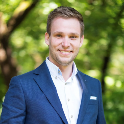
Hendriks, Rob

Hendriks, Rob
Program Lead
Holst Centre / TNO

Abstract
Impulse Printing™ is a brand new technology developed by Holst Centre that will bring unique 3D interconnect solutions to the back-end semiconductor and display market. High resolution structures can be printed over steps, gaps, and even wrapped around substrates at incredible speeds. For example, wrap-around printing of electrodes to create a back-to-front interconnect for µLED displays, or printing directly on silicon dies as an alternative to wire bonding. Off the shelf materials such solder paste, conductive adhesive, silver micron flake ink, copper nanoparticle ink and dielectric ink have already been printed successfully, showing compatibility with a wide range of viscosities and particles sizes. The unique capability of printing almost any materials onto any type of topology makes Impulse Printing™ suitable for quick adoption into existing production lines.

Biography
Program Lead experienced in developing novel printing technologies in the field of hybrid printed electronics. Responsible for defining the overall strategy and leading the execution of innovative technologies, including ultra-high resolution printing, laser-assisted transfer, 3D printed electronics and photonic soldering. Driven by innovation and determined to take concepts to full industrial implementation. Over 10 years of experience working in research and start-up environment across the U.S. and Europe.

Advanced Packaging Conference
I To top
IBM Zurich IBM Zurich Curioni, Alessandro
Keynote Opening
Curioni, Alessandro

Curioni, Alessandro
IBM Fellow, Vice President Europe and Africa and Director IBM Research - Zurich
IBM Zurich

Curioni, Alessandro

Abstract
Coming Soon

Biography
Dr. Alessandro Curioni is an IBM Fellow, Vice President of IBM Europe and Africa and Director of the IBM Research Lab in Zurich, Switzerland. On top of being responsible for IBM corporate research in Europe, he leads global research in Security and the Future of Computing.Dr. Curioni is an internationally recognized leader in the area of high-performance computing and computational science, where his innovative thinking and seminal contributions have helped solve some of the most complex scientific and technological problems in healthcare, aerospace, consumer goods and electronics. He was a member of the winning team recognized with the prestigious Gordon Bell Prize in 2013 and 2015. His reserch interests now include AI, Big Data and novel compute paradigms, such as neuromorphic and quantum computing.Dr. Curioni received his undergraduate degree in Theoretical Chemistry and his PhD from Scuola Normale Superiore, Pisa, Italy. He started at IBM Research – Zurich as a PhD student in 1993 before officially joining as a research staff member in 1998, where he had several research and manager roles, including being the founding manager of the Cognitive Computing and Computational Sciences department. He is a member of the Swiss Academy of Technical Sciences

Smart and Green Manufacturing Summit
Imec Imec Peeters, Michael
Opening
Peeters, Michael

Peeters, Michael
VP of R&D for Connectivity
imec

Peeters, Michael

Abstract
Coming Soon

Biography
Michael Peeters is VP of R&D for Connectivity at imec. His previous experience as CTO for both the Wireline and Wireless business lines at (what is now) Nokia was built on the culture, enthusiasm, and love for technology and science that he got from his time at Bell Labs—and the principles of Free Inquiry bestowed on him by his Alma Mater, the Vrije Universiteit Brussel (VUB).During his research career starting with a Ph.D. in Applied Physics and Photonics from the Vrije Universiteit Brussel, he has authored more than 100 peer-reviewed publications, many white papers and holds patents in the access and photonics domains. An electrotechnical engineer by training, he is a senior member of IEEE and a Fellow of the VUB. Outside of work, his quest to discover the recipe for a perfect lasagna is balanced by bouts of long-distance running to offset the inherent caloric intake.

ITF Beyond 5G
Imec Imec Collaert, Nadine
Tech talk
Collaert, Nadine

Collaert, Nadine
Program Director High-Speed Analog/RF
imec

Collaert, Nadine

Abstract
Coming Soon

Biography
Dr. Nadine Collaert is program director at imec. She is currently responsible for the analog/RF program looking at heterogeneous integration of III-V/III-N devices with advanced CMOS to tackle the challenges of next generation mobile communication. Before that she was program director of the LOGIC Beyond Si program focused on the research on novel CMOS devices and new material-enabled device and system approaches to increase functionality. She has been involved in the theory, design, and technology of FinFET devices, emerging memories, transducers for biomedical applications and the integration and characterization of biocompatible materials. She has a PhD in electrical engineering from the KU Leuven and she holds more than 400 publications and more than 10 patents in the field of device design and process technology.

ITF Beyond 5G
Imec Imec De Simone, Danilo
EUV Lithography patterning: status and challenges towards High NA
De Simone, Danilo

De Simone, Danilo
Staff Member
Imec

De Simone, Danilo

Abstract
Nowadays, the device scaling driven by the Moore’s law is continuing by the deployment of the 0.33NA extreme ultraviolet lithography (EUVL) in high volume manufacturing for single print and multi-patterning schemes further driven by the need to improve cycle time and cost. To further simplify and improve EUV patterning reducing cost and enable 2nm technology and below, high NA EUV lithography is under development and in 2023 imec and ASML will open a high NA EUV Lab, where the first high 0.55NA scanner will be installed.At the same time, as the nanoscale is pushed further down, the stochastic nature of the patterning process becomes one of the major patterning roadblocks. To enable the high NA technology new knobs and faster learning cycles on patterning process development are needed to improve the process window and minimize the stochastic patterning defectivity issues. Lithography solutions can’t afford alone the stochastic challenges; thus, the etching and thin film processes become essential to holistically offer, together with the lithographic process, novel clean pattering solutions. This presentation will show the latest development on EUV patterning materials and their challenges and provide an insight status of overcoming these obstacles towards high NA.

Biography
Danilo De Simone holds a MS degree in chemistry from the university of Palermo (Italy) and has 22 years of experience in semiconductor R&D field. He led the development of lithographic materials for 90nm and 65nm NOR Flash devices for STMicroelectronics (STM) in Italy and covered the role of assignee at STM Alliance in France and STM in Singapore. In 2008, he joint Numonyx to lead the R&D development for lithographic materials and first 32nm double patterning for PCM devices. In 2011, he moved to Micron Technology to introduce 45nm phase-change-memory devices in HVM, and to develop patterning solutions for novel devices. In 2013, he joined the international nanoelectronics research center imec leading the research on patterning materials for EUV lithography. He is editorial board member of the Journal of Micro/Nanopatterning, Materials, and Metrology (JM3), member of SPIE committee for the Patterning Materials and Processes program and member of the International Advisory Board of the Photopolymer Science and Technology Conference (ICPST).

Materials Innovation
Imec Imec Rolin, Cedric
The environmental footprint of Si chip manufacturing
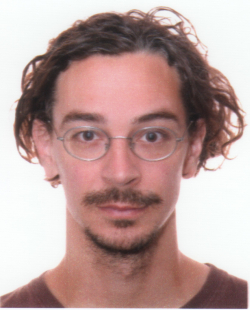
Rolin, Cedric

Rolin, Cedric
Program Manager
Imec

Rolin, Cedric

Abstract
The climate crisis calls for urgent actions towards sustainability as an integral component of businesses and regulations. With its large and growing environmental footprint, the Information and Communication Technology sector is arguably a large part of the problem, but also a part of the solution. Fabrication of integrated circuits is an energy and resource intensive process and the drive towards higher performance and increased functionality increases the process complexity dramatically from node to node. Traditionally, the improvement between technology nodes is evaluated using Power, Performance, Area and Cost (PPAC) metrics in a Design Technology Co-Optimization (DTCO) completely neglecting sustainability. However, this established framework provides an opportunity to do early sustainability assessments of future technologies all the way from material sourcing and fabrication to end of life. To demonstrate this approach, we evaluate the environmental impact, more specifically the energy, ultra-pure water (UPW) and mineral consumption as well as the greenhouse gas (GHG) emissions from manufacturing logic, DRAM and NAND technologies from past to future nodes. Our analysis of logic scaling reveals how the environmental metrics normalized per transistor evolve along with improvements in performance and reduction in cell area.

Biography
Cédric Rolin is Manager for the Sustainable Semiconductor Technologies and Systems (SSTS) Program at imec. He received his M.S. degree and his PhD degree in materials science from the Université Catholique de Louvain in 2004 and 2009 respectively. During the first 13 years of his career (including 2 years postdoc at University of Michigan), Cedric grew his expertise in the thin film growth and manufacturing of devices based on organic semiconductors. Then, from 2018 to 2021, he led a R&D team developing solutions to move flexible thin film circuit and display technologies from the Lab to the Fab. Part of this effort focused on the upscaling of the nanoimprint lithography patterning technology to a 300mm Fab tool. Since November 2021, Cédric has joined the sustainability effort of imec as Program Manager, focusing on the assessment and improvement of the environmental footprint of the semiconductor manufacturing industry.

Smart and Green Manufacturing Summit
Imec Imec Van den hove, Luc
Deep tech: the lodestar to meet the challenges of the 21st century.
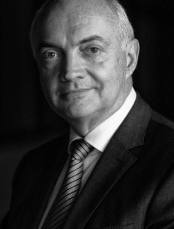
Van den hove, Luc

Van den hove, Luc
President and CEO, imec
Imec

Van den hove, Luc

Abstract
Deep tech, enabled by semiconductor technology, will provide disruptive innovations that are essential for tackling humanity's monumental challenges. For example, the world needs a transformation in medicine to address current and future challenges. Many virologists believe that the likelihood of future pandemics is increasing, so we must act now to be prepared for the future. By leveraging the most recent technological advances, we can radically transform medicine to protect the world from future pandemics. Medicine will become digital, enabling vital advancements, including decentralized and low-cost personalized drug and vaccine production. However, the challenges to realizing these critical advancements are enormous. Just as Moore’s law drove the semiconductor industry to respond to increasing computing and storage challenges, we could accelerate medical innovations by a technology roadmap where technology platforms are developed pre-competitively. The transformation of medicine will require the handling and analysis of exponentially growing amounts of data, demanding enormous computing power. And healthcare is just one of the many new application areas which will depend on the exponential growth of data. To enable this sustainably, we need an even more aggressive semiconductor roadmap than what we have achieved over the last decades. At imec, we have proposed a roadmap on how we can continue to enable more performant semiconductor technologies. And we will leverage our core semiconductor expertise to realize deep-tech innovations by co-innovating at the semiconductor technology level, the system and application levels, and by leveraging expertise from many domains such as material science, biomedical, pharma, AI, and others. Building flourishing deep-tech ecosystems must become a priority to meet the challenges of the 21st century.

Biography
Luc Van den hove is President and CEO of imec since July 1, 2009. Before he was executive vice president and chief operating officer. He joined imec in 1984, starting his research career in the field of silicide and interconnect technologies.In 1988, he became manager of imec’s micro-patterning group (lithography, dry etching); in 1996, department director of unit process step R&D; and in 1998, vice president of the silicon process and device technology division. In January 2007, he was appointed as imec's EVP & COO. Luc Van den hove received his PhD in electrical engineering from the KU Leuven, Belgium.He has authored or co-authored more than 200 publications and conference contributions.

Executive Forum
INFICON INFICON Bode, Christopher
Predictive Maintenance Scheduling for Assembly Manufacturing
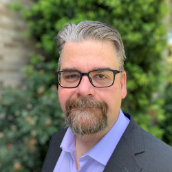
Bode, Christopher

Bode, Christopher
Technical Product Manager
INFICON

Bode, Christopher

Abstract
The semiconductor industry and its struggles with supply chain issues have made the global news almost daily. Tactical options to address issues with existing manufacturing assets include getting more capacity out of existing fabs and/or enabling fabs run a broader mix of technologies and products for a longer period. Factory automation capabilities are certainly a necessary solution to facilitating such improvements, whether in terms of maximizing tool availability or manufacturing productivity. Assembly facilities are beginning to adopt such solution in volume from their front-end manufacturing counterparts to good effect. Smart Manufacturing solution integration is increasingly demonstrating the capability to move beyond point solution development in back-end facilities to deliver differentiating capabilities in manufacturing efficiency and productivity. This talk will discuss examples of harmonizing deployed solutions to facilitate predictive maintenance scheduling through the integration of tool control and factory scheduling.INFICON has deployed Smart Manufacturing capabilities to a customer Assembly site that demonstrates the end-to-end solution and business process integration of a predictive maintenance capability. FabGuard® Fault Detection and Classification (FDC) is deployed on a Disco grinder tool to monitor a number of tool parameters for general tool control capability, but also monitors the blade thickness over time to predict when a blade replacement will be needed. Such information is shared with the factory Digital Twin to support overall factory modeling and prediction capability. Factory Scheduler, in addition to performing the nominal responsibility of scheduling material to be run on each of the tools, can consume the FDC data and maintenance prediction to schedule an optimal time to perform the tool maintenance given operator and tool availability. The shared decision support with the integrated solution makes it so that the parts and assignment of duties can be done ahead of time, minimizing tool downtime and maximizing maintenance efficiency. The presentation will discuss the deployment and impact of these solutions as deployed in our customer facility.

Biography
Christopher Bode, PhD is a recognized process control and factory automation solition developer within the semiconductor industry. He has over 25 years experience with APC technology development and implementation, as well a general factory systems development and integration across solution domains, with prior stints at AMD and GLOBALFOUNDRIES. He currently is a Technical Product Manager with INFICON in their Intelligent Manufacturing System organization, with responsibilities across their FabGuard (TM) and FPS product lines.

Advanced Packaging Conference
Infineon Infineon Knott, Bernhard
Innovative Sensor Packaging in Europe

Knott, Bernhard

Knott, Bernhard
Head of the Infineon Technologies Backend Innovation Group
Infineon

Knott, Bernhard

Abstract
The presentation will include topics like: eWLB radar (fan-out WLP at Infineon Regensburg); Pressure sensors e.g. for automotive; Magnetic sensors and Gas sensors.

Biography
Bernhard Knott is the Head of the Infineon Technologies Backend Innovation group. He is responsible for new Package Concepts, Prototyping, new Materials, Simulation and Virtual Prototyping. Until 2016 he was leading the Package Development for Sensors and Waferlevel Package Development in Regensburg, Germany. Prior joining the Backend Organization, he held several Management Position in Frontend Technology dealing with BiCMOS Technologies, Sensors and Innovation projects. After receiving his Diploma in Physics from the University of Regensburg, he started his career in Semiconductor Industry in 1997 in developing an embedded NVM Technology. Bernhard holds several patents and patent applications in the area of FE Technology, Sensors and Packaging.

Advanced Packaging Conference
Infineon Technologies AG Friedrichs, Peter
SiC Power Technologies and business – empower a greener future

Friedrichs, Peter
Vice President SiC
Infineon Technologies AG

Abstract
SiC power devices have shown a tremendous growth over the last few years, targeting to a multi-billion dollar business by the end of the decade. Many driving applications belong to the segment of emerging applications related to the electrification of mobility and enhanced use of green energy. Those new applications, however, might need device solutions which differ substantially from the known portfolio based on silicon. One trend is for instance a much wider range of rated blocking voltages in order to be more application specific. The presentation will explain this trend in more detail and give concrete examples how such an adapted portfolio impacts the future of wide band gap power semiconductors.

Biography
Dr. Peter Friedrichs received his Dipl.-Ing. in microelectronics from the Technical University of Bratislava in 1993and his Ph.D work at the Fraunhofer Institut FhG-IIS-B in Erlangen. His focus area of expertise was the physics of the MOS interface in SiC. In 1996 he joined the Siemens AG and was involved in the development of power devices on SiC.Peter joined SiCED GmbH & Co. KG, a company being a joint venture of Siemens and Infineon, on March the 1st, 2000. Since July 2004 he was the managing director of SiCED. In 2009 he achieved the Dipl.-Wirt.-Ing. From the University of Hagen. After the integration of SiCED’s activities into Infineon he joined Infineon on April 1st, 2011 and acts currently as Vice President SiC.

Electrification & Power Semiconductors
Intel Corporation Intel Corporation Scheper, Frans
Building Europe’s Digital Future - A Pan European Investment

Scheper, Frans

Scheper, Frans
President & General Manager EMEA
Intel Corporation

Scheper, Frans

Abstract
Building Europe’s Digital Future - A Pan European Investment

Biography
Frans Scheper is the Corporate Vice President in the Sales, Marketing, and Communications Group, General Manager and President for Europe, Middle East, and Africa (EMEA) for Intel Corporation. He is responsible for Intel's overall business in EMEA which includes driving revenue growth, engaging with the local ecosystem to create new opportunities, and strengthening Intel's existing regional customer and partner relationships. Frans is also in charge of overseeing Intel's IDM 2.0 strategy across Europe, with research, design, leading-edge semiconductor manufacturing, and industry that will help build Europe's digital future.Prior to Intel, Frans was Chairman and Executive Vice President of Opto Semiconductors at ams OSRAM, and has also held executive board positions at WeEn Semiconductors, NXP Semiconductors, and the CEO position at Nexperia.

Advanced Packaging Conference
Intel Corporation Intel Corporation Brady, Todd
Intel RISE2030 and 2040 carbon neutral goals
Brady, Todd

Brady, Todd
Director, Global Public Affairs and Sustainability
Intel Corporation

Brady, Todd

Abstract
Coming Soon

Biography
Todd Brady is the Director of Global Public Affairs and Sustainability for Intel Corporation. In this role he leads state and local government affairs, media and community relations, corporate volunteerism and sustainability at the company's major manufacturing and office locations around the globe. In addition to overseeing regulatory and community engagement strategies in the US, China, Southeast Asia, Israel, Ireland and Latin America, he directs Intel’s global initiatives to make Intel “smart & green” by leading corporate-wide sustainability programs such as climate, energy and water conservation, green design and the integration of internet of things (IoT) solutions to create smart and green offices, buildings and facilities of the future. During his 20+ years at Intel, Todd has represented the company publicly in numerous forums and led industry-wide initiatives in many national and international committees. He has authored more than 20 papers in scientific journals and conference proceedings on a variety of sustainability topics. In 2009, he was named by Scientific American as one of ten outstanding leaders involved in research, business or policy pursuits that have advanced science and technology. Todd holds a BS in Chemical Engineering from Brigham Young University and a MS in Environmental Engineering from the University of Illinois at Urbana-Champaign.

Smart and Green Manufacturing Summit
ISRL ISRL Zabelinsky, Ilya
Time to Collaborate. SubFAB Research and Development
Zabelinsky, Ilya

Zabelinsky, Ilya
Co-Founder
ISRL

Zabelinsky, Ilya

Abstract
The ChallengeThe Semiconductor Industry’s desire for sustainable manufacturing has many challenges to overcome before environmental targets set by most companies can be trustfully met with meaningful positive impact on Global climate changes.One of the key areas poised to become a showstopper for the industry’s ability to achieve sustainability goals is commonly called SubFAB. The SubFAB is a variety of equipment and technologies designed to handle process materials from tool chambers to the factory’s exhaust stacks.Existing infrastructure and siloed approach for SubFAB equipment and technologies R&D can’t support true game changing development of environmentally friendly and affordable solutions to match the manufacturing technologies advancement cadence.This sector is traditionally underserved by fundamental academic research and typically fails to compete for Fab equipment downtime, especially these days when chips shortage keeps factories fully loaded.Chipmakers are forced to spend more capital money on manufacturing capacity and face skyrocketing operational costs. Equipment manufacturers are struggling to meet customer requirements for equipment uptime and Hazadous Air Polutant (HAP) emissions. At the same time academic institutes aren’t involved in research of chemistry and physical nature of post-process material handling.The OpportunityInternational SubFAB Research Labs (ISRL) strategic initiative is being formed these days to pull in an industry-wide collaborative effort on a mission to Bring the Science to SubFAB” and supplement Semiconductor manufacturing technologies advancement with focused research of unwanted and harmful side effects caused by unreacted process materials downstream from process chambers.Member companies will gain access to dedicated facility with complete infrastructure required to operate a set of 300mm process tools with versatile setup of deposition and dry etching process chambers at HVM-like conditions to supplement research and development projects.ISRL will provide its partners a unique opportunity to participate in fundamental research and gain access to common IP or alternatively invest in development of company specific solutions with compartmentalized IP.ISRL will have highly skilled project teams to lead scientific research focusing on reliability issues, technology validation, pathfinding, materials handling and reclaim. Facilities setup will enhance practical skills acquisition for workforce development.

Biography
Ilya Zabelinsky is a globally recognized Technical Leader with over 25 years of experience in vacuum and gas abatement applications for Semiconductor manufacturing.Ilya joined Intel in 1996 to take part in startup and commissioning team of first 200mm fab in Israel, moving on to develop his career as operational and technical leader through several technology node transitions and manufacturing capacity expansion projects. In 2006 Ilya spearheaded an effort to install and commission a full set of vacuum and gas abatement systems for a greenfield construction of 300mm Fab in Kiryat Gat, extending his operational and technical leadership to entire SubFAB ecosystem supporting technology transitions and capacity expansion projects from 45 to 10nm.In April 2022 Ilya left Intel on a mission to “bring the Science to SubFAB” by supplementing Semiconductor manufacturing technologies advancement with focused research of unwanted and harmful side effects caused by unreacted process materials downstream from process chambers.In May 2022 Ilya co-founded International SubFAB Research Labs (ISRL).Ilya possesses broad knowledge and vast practical experience in wide range of semiconductor manufacturing processes, FAB equipment, central facilities systems and infrastructure, spanning from scope definition, programming and design through construction, commissioning and operations. Ilya holds a B.Sc in Chemical Engineering from SCE, Israel. Ilya is passionate practitioner of various education and mentoring programs aimed at new generations of professional and diverse workforce.

Innovation Showcase
K To top
Kontron-AIS GmbH Kontron-AIS GmbH Mueller, Bert
Sensor Integration Framework with Interface A
Mueller, Bert

Mueller, Bert
Head of Business Unit System Integration
Kontron-AIS GmbH

Mueller, Bert

Abstract
Within the last few years, semiconductor, photovoltaic or HB-LED industry developed enormously. With the result that the complexity of almost all relevant processes increased. To prevent the increase of corresponding costs, a concept of Equipment Engineering Systems (EES) is essential. Integrating applications like Equipment Data Control, Advanced Process Control (APC) and Fault Detection Control (FDC) is fundamental to improve product yield and reduce manufacturing costs. Nevertheless, adapting APC solutions to relevant processes in semiconductor, photovoltaic or HB-LED factories remains a huge challenge.To accomplish efficient machine integration of technical data, which is the basis for APC applications, internationally standardized and high-efficient interfaces are obligatory. In addition to the already established SECS interface, which also has established itself during recent years as PV02 interface in the PV industry, first results from high volume productions show that these interface technologies are not enough. They must be supplemented to meet the high data volume and the flexible adjustments. A few years ago, the SEMI Organization has defined the Interface A Standard which should give an answer to the named problems. In addition to its modern and highly efficient software technology, functional properties like the Interface A self-description make this standard very interesting for APC applications for high-efficient designed FAB’s because a very strong motivation is to make the process engineer independent of the IT-Department. They need solutions which enable the engineer to configure the data stream online. The amount of data and their frequency must be defined at the time of their needFor this reason, making an effort to implement the Interface A technology as an embedded solution in other software components, certainly can be a useful strategy. In particular, the ability to synchronize sensor data, process data and logistic parameters makes this approach very interesting. This paper presents a framework to simplify the interface between a variety of external sensors and consumer devices. These abstractions facilitate a componentized framework that allows developers to focus on writing minimal pieces of sensor-specific code enabling an system of reusable sensor drivers.

Biography
Dipl.-Ing. Bert MuellerCompany: Kontron-AIS GmbHPostion in the Company: Head of Business Unit System Integrationprofessional career:1995 diploma in Automation Technology, received from TU Dresden1995-2000 AIS Automation Dresden GmbH as SW Developersince 2000 Kontron-AIS GmbH as Head of Business Unit

Thursday Innovation Showcase
L To top
LineLab LineLab Nietner, Larissa
LineLab, an Analytical Tool for Modeling Semiconductor Manufacturing Systems
Nietner, Larissa

Nietner, Larissa
Cofounder
LineLab

Nietner, Larissa

Abstract
Semiconductor production systems have traditionally been difficult to model and optimize. Nonlinear queueing behavior and tools handling dozens of processes introduce great complexity to the dynamics of variation and inventory in a fab. As a result, only Monte-Carlo methods, like discrete-event simulation, could capture the relationships between capacity, queueing, utilization, inventory, and throughput that govern operations and performance. Since any simulation run only offers a single-point solution, optimizing a fab for a new device often requires months of simulation.We have developed an analytical method that captures these complex system dynamics, and are commercializing it in a new software tool called LineLab. The first true alternative to Monte-Carlo simulation for modeling complex fab systems, it enables a breadth of new analyses and significantly accelerates the development timeline. To create LineLab’s powerful solver, we developed prescriptive analytics for queueing systems, and are using an optimization technique that is capable of handling the nonlinear relationships, alongside detailed financial models. For fabs of any complexity, LineLab can optimize capacity, buffers and utilization of each high-value tool, work-in-progress inventory and flow time / cycle time, minimizing total unit cost. LineLab considers the cost of inventory as it optimizes queue sizes, accounting for wafers’ value-add with every process. Our approach can capture any level of flow complexity, including re-routing wafers through the same tool many times with intermediate steps, inbound flows and quality, capturing the effects of process time variability. It can also capture the interaction of parallel product flows and determine the effective cost of adding a new product to a shared system in a foundry. With our analytical approach, the complete sensitivity data for every input are known at all times. Coupled with the ability to specify inputs with uncertainty, LineLab reveals the key performance drivers and risks across the entire system encompassing design, process models, and fab operations. LineLab can determine the marginal cost of variability, design parameters, and any other input. The approach also allows for parametric models capturing Scope 1 & 2 CO2, water usage and other sustainability metrics.An MIT spinout, LineLab is the first tool to optimize complex queueing systems, and it captures their dynamics with a very high degree of accuracy (>99%).

Biography
Dr. Larissa Nietner is cofounder of LineLab, a spin-out from MIT. She received her Masters and Ph.D. in Mechanical Engineering from the Massachusetts Institute of Technology (MIT) after obtaining a B.Eng. in her native Germany. Dr. Nietner has presented at the Flex Conference (now part of SEMI) and given a number of invited talks at universities in the US and Europe. After completing her Ph.D., she held a postdoctoral position at MIT’s Sloan School of Management in the Operations Research Group joining Dr. Scott Nill, where she worked on the new modeling framework that makes up LineLab. Together, they spun out LineLab, releasing the launch version of the software in 2021, and continue to co-author peer-reviewed papers about the approach and the far-reaching new analyses it enables.

Fab Management Forum
M To top
McLaren Applied McLaren Applied Lambert, Stephen
High Performance 800V Silicon Carbide Inverters for Automotive Applications: The Next Step in Electrification?
Lambert, Stephen

Lambert, Stephen
Head of Electrification
McLaren Applied

Lambert, Stephen

Abstract
McLaren Applied have been developing ground breaking solutions for electrification in both Automotive and Motorsport for over a decade. The culmination of these developments is its IPG5 800V Silicon Carbide Inverter, which represents the next step in Electrification – particularly in highly efficiency drivetrains, key for the next wave of electrification.

Biography
Dr Stephen Lambert received his Doctorate from the University of Warwick by looking at the applicability of hybrid and electric drivetrains in motorsport. Following this he worked at Lotus Engineering, developing hybrid and electric demonstrator vehicles for a number of OEMs. Through this role, he found himself working closely with battery manufacturers as a key partner for these projects. He has since worked in various roles around developing battery technology in areas such as Formula 1 and high performance road cars. He is now responsible for the electrification strategy for automotive customers with McLaren Applied technologies, where he is helping deliver advantage by empowering customer to introduce and protect new vehicle concepts and technologies and to drive differentiation in the market. He is also chairman of ASEIN, a dedicated UK initiative focused on the accelerated and advanced delivery of Electronic Systems (ES) into vehicles and infrastructure operated by the UK Trade Association – TechWorks.

Smart Mobility
Melexis Melexis Chombar, Francoise
Accelerating Gender Balance in the Semiconductor Talent Pool
Chombar, Francoise

Chombar, Francoise
Chairwoman
Melexis

Chombar, Francoise

Abstract
Coming soon

Biography
Françoise Chombar is Chairwoman and co-founder of Melexis. She served as the CEO of Melexis for 18 years (from 2003 to 2021). She is currently a member of the Board of Umicore, the Board of Soitec, Chairwoman of the Board of BioRICS and member of the advisory Board to Byteflies. From May 1 2022 onwards, she will join the Board of Antwerp Management School. She is equally president of the STEM platform, an advisory board to the Flemish government, aiming to encourage young people to pursue a Science, Technology, Engineering, or Mathematics education. Françoise Chombar’s long-term commitment to actively advocating more STEM and more gender balance is driven by the profound belief in their positive societal impact. She is the recipient of numerous awards including the Vlerick Award, the Global Prize for Women Entrepreneurs of BNP Paribas, ICT-Personality of the Year by Datanews, Science Fellowship at the VUB, Honorary Award by the Flemish Community, the Computable Lifetime Achievement Award and a Honorary Award by the KUL. Ms. Chombar holds a Master’s Degree in interpreting (Dutch, English, and Spanish) from Ghent University.

The Future of Work
Merck KGaA Merck KGaA Matz, Laura
Keynote Presentation
Matz, Laura

Matz, Laura

Merck KGaA

Matz, Laura

Abstract
Coming soon

Biography
Dr. Laura Matz is the Chief Science and Technology for Merck, driving innovation and digitalization in Merck across the 3 business sectors, Life Sciences, Healthcare and Electronics. Serving as an executive vice-president within Merck, she is responsible for the corporate innovation teams including the digital office and new digital business models. She possesses 20 years of experience in semiconductor manufacturing and a decade of experience running semiconductor materials businesses.Prior to becoming the CSTO, she was a senior vice-president within EMD Electronics (previously Versum Materials and Air Products Electronics division). She has always been a key contributor to the growth in semiconductor materials, driving for a strong R&D presence to enable business growth. Laura is a strong advocate for science and engineering in young talent. She has collaborated with ASU over the past 5 years to build a strong pipeline of interns. In 2020, Laura joined the AICHE (American Institute of Chemical Engineers) ILI board (Institute for Learning and Innovation) which serves as a conduit for advancing chemical engineering talent for the U.S. Given that artificial intelligence and machine learning are enablers for the continued growth in the semiconductor industry, she is a member of the SEMI Smart Manufacturing committee as well as the local AZ SEMI committee.Laura has a PhD in analytical chemistry from Washington State University and undergraduate degree from Indiana University of Pennsylvania. When she is not working, Laura enjoys watching soccer games and running in the beautiful Arizona weather.

Executive Forum
MSV Systems & Services Pte Ltd MSV Systems & Services Pte Ltd Tan, Joe
Keep It Simple & Save (KISS) in Burn-In Operations
Tan, Joe

Tan, Joe
Founder & Managing Director
MSV Systems & Services Pte Ltd

Tan, Joe

Abstract
Typical semiconductor burn-in operations have multiple burn-in systems, auto-loaders & a huge quantity of burn-in boards on racks or trolleys.Limited integration between equipment had resulted in significant manual handling activities, which in turns had caused low OEE, high maintenance & high resource wastages.While many companies had attempted to automate the burn-in operations through the use of robotics & AMR, the cost of both implementation & maintenance is prohibitive. Moreover, there are little efficiency gain with these attempts & operational flexibility can be significantly compromised.This presentation showcase how a small change in the burn-in chamber design based on our patented MudaX solution, can help companies Keep It Simple, solves most, if not all the operational challenges in burn-in & Saves significant cost in burn-in operations.This presentation has very recently won the Most Inspirational Presentation award in TestConX USA conference in Arizona in May 2022.

Biography
Joe Tan is the Founder & Managing Director of MSV Systems & Services Pte Ltd established in Singapore in 2002.He graduated from the National University of Singapore with a Honours Degree in Electronics Engineering & a Master’s Degree in Industrial & System Engineering.After over 20 years of providing technical service on burn-in systems, auto-loaders & burn-in boards. MSV had invested in R&D & patented the MudaX solution to help companies Keep It Simple & Save (KISS) in burn-in operations.

Innovation Showcase
N To top
Newcastle University O'Neill, Anthony
Improving 4H-SiC MOSFETs by Gate Engineering
O'Neill, Anthony

O'Neill, Anthony
Professor
Newcastle University

Abstract
Metal Oxide Semiconductor (MOS) interfaces have been a major challenge in the fabrication of SiC MOSFETs. This has resulted in poor MOS electrical performance with electron mobilities below 10 cm2/V.s compared with bulk values close to 1000 cm2/V.s. Restricted MOS gate stack reliability means that an upper temperature limit of 150 °C is imposed by leading manufacturers of SiC power MOSFETs, despite 4H-SiC having an energy bandgap of 3 eV, compared with just 1 eV for Si. High-performance 4H-SiC lateral MOSFETs have been fabricated, with a peak effective mobility of 265 cm2/V.s in 2 μm gate length MOSFETs. The gate-stack was designed to minimize 4H-SiC/SiO2 interface defect states and comprised a thin 0.7-nm thermally grown SiO2 on 4H-SiC, followed by a deposited dielectric and a gate contact. In this way, residual carbon relate defects following SiC oxidation are significantly reduced. A density of interface traps (Dit) in the range of 6 × 10¹¹ – 5 × 1010cm−2eV−1 is thus obtained, a reduction of 100x compared with a conventional gate stack with a thermally grown thick oxide.

Biography
Anthony O'Neill is Siemens Professor on Microelectronics at Newcastle University, having joined in 1986 from Plessey Research (Caswell) Ltd. He is well known for pioneering work in strained silicon, which improves CMOS electronics performance without shrinking dimensions. It’s still used in most electronic systems today, from smartphones to server farms. Since then he has re-engineering SiC MOSFETs to achieve record electrical performance with channel resistance now approaching Si. He has held visiting appointments at MIT, EPFL, Monash University and Atmel.

Electrification & Power Semiconductors
Niching Industrial Corp. Niching Industrial Corp. Dong, Rui-Xuan
Ultra low-temperature silver sintering materials for substrate-based power applications

Dong, Rui-Xuan
Project Leader
Niching Industrial Corp.

Dong, Rui-Xuan

Abstract
The demand of high powder semi-conductor devices is increasing continuously. Especially for wide band gap (WBG) semiconductors, the die-attach (DA) materials need to be bonded at a lower temperature,200 oC ideally, and operated at a high temperature (~300oC). Low-temperature sintering silver provides excellent properties to meet the requirement of DA materials on WBG applications. The common sintering temperature of commercial products is > 200dC. High sintering temperature generates a higher level of thermal stress in the DA materials, which would cause negative effects for larger dies, including void generation, delamination, crack, metallization peeling, and so on. Lower sintering temperature could reduce thermal stress during packaging processes. In addition to 200-oC sintering Ag paste (DN-1206Q), we have developed DA Ag paste with 175-oC sintering temperature (DN-1301A) for the requirement of low stress. This article is investigating the effect of sintering temperature on the performance and properties of DA materials.The storage modulus of 175oC (DN-1301A) and 200oC (DN-1206Q) sintering Ag paste are 14 and 18 GPa respectively. This is more than 20% reduction which could be a great help in terms of thermal stress. As for die shear strength (DSS), DN-1301A showed comparable results while curing at 175 oC comparing with DN-1206Q curing at 200 oC. Thermal conductivity (TC) of both 175 and 200-oC sintering Ag paste is more than 120 W/mk. In summary, lower sintering temperature can reduce the thermal stress of DA materials which is a positive contribution to the resistance of temperature variations. The performance of DN-1301A curing at 175 oC is similar to 200oC sintering Ag paste (DN-1206Q). Based on this study, it is very promising that a lower sintering temperature at 175 oC for silver sintering paste can deliver similar performance as curing at 200 oC. This could be a breakthrough for those requiring lower curing temperature such as laminate substrate-based packages.

Biography
2006-2010 Ph.D, Institute of Polymer Science and Engineering, National Taiwan University.2014-2016 Researcher, Industrial Technology Research Institute2016-2019 R&D Manager, New Micropore, Inc.2019-Now R&D Project Leader, Niching Industrial Co.

Advanced Packaging Conference
Nokia Nokia Ziegler, Volker
Panelist
Ziegler, Volker

Ziegler, Volker
Senior Technology Advisor & Chief Architect
Nokia

Ziegler, Volker

Abstract
.

Biography
Volker is an energetic leader with 25+ years of broad and international experience in the telecommunications industry. He currently serves as Senior Technology Advisor and Chief Architect in Nokia Strategy and Technology unit. Previously, Volker has exercised a leadership role with Nokia Bell Labs in 6G research and ecosystem and has served as Head of 5G Leadership and Chief Architect of Nokia Mobile Networks. Prior to this, Volker has been active in the Head of Strategy role of Nokia Siemens Networks where he had also served as the Head of the North East Region. In his 10+ year career with Siemens, Volker has held business unit leadership, finance, sales and marketing, services and R&D global roles and senior positions. He has worked as Information Technology Specialist with the World Bank / IFC in the mid-90s. Volker has started his career as a research scientist with German Aerospace Research / DLR. Volker holds a Dr.-Ing. (PhD) degree in Electrical Engineering from Technische Hochschule (TH) Karlsruhe in Germany and is a graduate of the Executive Development Program at Harvard Business School.

ITF Beyond 5G
Nova Ltd Nova Ltd Szafranek, Dana
Spectral Interferometry (SI) And Vertical Traveling Scatterometry (VTS) Technology For Advanced Metrology Of Back-End-Of-Line (BEOL) Manufacturing Process Steps
Szafranek, Dana

Szafranek, Dana
Algorithm scientist
Nova Ltd

Szafranek, Dana

Abstract
We present advances in optical critical dimension (OCD) metrology for back-end-of-line (BEOL) manufacturing process steps. Semiconductor device fabrication has advanced rapidly in recent decades, in part due to OCD metrology. Standard techniques for OCD are either spectral reflectometry and/or ellipsometry (SR/SE). We present here a new technology – Spectral Interferometry (SI)- implemented on the Nova PRISM OCD platform as a unique capability in Nova’s high-end Stand-Alone metrology solution portfolio. SI extracts unique spectral information from the sample, inaccessible by current technologies. To complement Nova PRISM, the SI data is processed with a novel algorithmic suite called Vertical Travelling Scatterometry (VTS). VTS enables selective OCD analyses of the top part of a sample separately from the bottom part of a sample within a single metrology step. Thus, it is possible to focus selectively on the topmost layers of interest to simplify the complexity of traditional OCD modeling. Multiple benefits include enhanced robustness by controlling metrology consistency under incoming variations, reduced time-to-solution due to the simplified geometry, and feasibility of modeling complex in-die applications. Recent developments in the fabrication of logic circuits and memory elements require advanced dimensional metrology steps very late in the semiconductor production process, e.g., in the back-end-of-line (BEOL) process steps where it was previously not required. Moreover, the varied topology of the samples renders metrology of the fully integrated device, i.e., metrology “in-die”, preferable, rather than using a dedicated metrology target in the scribe line. However, an “in-die” sample with many layers and buried three-dimensional architectures introduces many degrees of freedom to traditional OCD that represent the cumulative possible process variations. As a result, traditional OCD approaches based on scatterometry may not be capable of the required precision for tight process control of the BEOL process steps. It is especially beneficial to apply SI and VTS for such BEOL applications, since the separation of “relevant” and “irrelevant” information correlates to the depth of the optical signal, and thus simplifying the resulting geometric die model.

Biography
Dr. Szafranek is an algorithm developer within the semiconductor industry. Earlier in her career, she focused on computational methods for electromagnetics. In recent years, Szafranek took part in projects involving machine learning, data augmentation, feature extraction, etc., while always keeping herself minded towards the underlying fundamental physics and full physical modeling.

Innovation Showcase
O To top
Oxford Instruments Plasma Technology O'Mahony, Aileen
A reliable manufacturing solution to enable normally-off recessed gate GaN MISHEMT by atomic layer etch and in-situ etch depth monitoring
O'Mahony, Aileen

O'Mahony, Aileen
Product Manager
Oxford Instruments Plasma Technology

Abstract
GaN HEMTs for power electronics applications is projected to be a $1b market by 2030 and is a critical enabling technology in some very high growth markets like USB-C fast-chargers, automated vehicles and datacentres. The benefit of GaN HEMTs for these applications is that they deliver high breakdown field, high-temperature operation, and their strong spontaneous and piezoelectric polarization-induced 2D electron gas (2DEG) of high carrier density and mobility. There are multiple device geometries and production routes to commercialising these more efficient, higher operating temperature, smaller, lighter, and lower cost GaN-based power semiconductors. However, a key attribute for power applications is that the GaN HEMT is “normally-off” in operation for safety and fail-safe requirements. One device solution that meets these requirements is the recessed gate GaN MISHEMT. A critical technology challenge is to ensure that the recessed gate is formed by etching to reliably and repeatably leave a thin (<5 nm) layer of AlGaN with an accuracy of ±0.5 nm. We present data demonstrating our low damage, and repeatable atomic layer etch process that has been validated by an optimised in-situ endpoint monitoring solution to achieve this AlGaN thickness accuracy. In addition, the recessed gate GaN MISHEMT device has achieved normally-off behaviour delivering a viable solution for this device geometry in high volume manufacturing.

Biography
Aileen O’Mahony is an Atomic Scale Processing Product Manager at Oxford Instruments Plasma Technology. Aileen has a PhD in Chemistry from University College Cork, Ireland, in the field of Atomic Layer Deposition (ALD) for microelectronics applications. Aileen has worked in the US and UK on industry-driven process development for the commercialisation of ALD-functionalised products and is now focused on advancing Atomic Scale Processing product solutions at Oxford Instruments. She is the author and co-author of over 20 publications, and has presented at numerous international conferences and workshops.

Thursday Innovation Showcase
P To top
PEER Group PEER Group Suerich, Doug
Treading lightly: How a pandemic pivot to remote integrations helped reduce our carbon footprint
Suerich, Doug

Suerich, Doug
Product Evangelist
PEER Group

Suerich, Doug

Abstract
When the pandemic hit its disruptive peak in 2020-21, the airline industry took a record-breaking tumble as countries restricted travel to limit the spread of COVID-19. For PEER Group, a company that supplies automation software to semiconductor OEMs and factories around the world and relies on onsite discovery, integration, and inspection to deliver and maintain its products, the limitation on international travel forced an immediate pivot to alternative ways of performing these critical functions.As the business world moved to remote work and virtual communication platforms to stay connected with colleagues and customers, so too did PEER Group’s integration and services team to ensure clients and partners continued to receive the same high level of service they were accustomed to pre-pandemic.In this presentation, we’ll share lessons learned from two years of performing remote discoveries, integrations, and inspections and how, in some instances, these lessons have become best practices for our customers going forward. We’ll show how pivoting specific functions to remote platforms has decreased our reliance on air travel, reducing PEER Group’s carbon footprint during the pandemic and, as we continue to improve and develop our remote capabilities, into the future.

Biography
Doug Suerich, Director of Marketing & Product Evangelist, PEER GroupDoug combines more than 20 years of experience creating manufacturing software with a deep desire to help customers find the best solutions to solve their biggest challenges. A passionate advocate for smart manufacturing, Doug is an active member of the SEMI SMART Manufacturing Technology Community, Americas Chapter, and co-chairs the Advanced Process Control Smart Manufacturing Conference.

Smart and Green Manufacturing Summit
PhotonDelta PhotonDelta Penning de Vries, René
Next generation microchips, powered by light
Penning de Vries, René

Penning de Vries, René
Chairman of the Supervisory Board
PhotonDelta

Penning de Vries, René

Abstract
Coming soon

Biography
Coming soon

Integrated Photonics
R To top
Robert Bosch GmbH Beer, Leopold
Semiconductors for Software Defined Vehicles
Beer, Leopold

Beer, Leopold
VP Product Management ASIC's & SOC's
Robert Bosch GmbH

Abstract
The importance of SW in Automotive is constantly increasing and currently we are reaching a point where its justified to talk about software defined vehicles.In his talk, Leopold will elaborate why semiconductors became a special focus topic for automotive OEM's and what this means for the traditional automotive semiconductor and system suppliers. At this stage of evolution, traditional, hirarchical supply chains restructure into to supply networks - opening up opportunities for new players.Based on technology requirements, Leopold will show how this new structures could look like and which are the new Key Succes Factors for the involved players.Leopold will use real life examples to explain the way Bosch Automotive Electronics addresses this topic.

Biography
Mr. Leopold BeerVP Product Management ASIC’s and SOC’s within the Bosch Automotive Electronics Division.Leopold Beer graduated the University of Stuttgart with a diploma in Physics. He specialized in semiconductor physics.Leopold started his career as engineer in the DRAM plant of Siemens Semiconductors (Today Infineon Technologies) in Regensburg and since then held various functions in the automotive and semiconductor industry.Leopold joined Bosch Sensortec in 2006 as Director of Sales and was later on promoted to Head of Global Marketing and Product Management. From 2013 to 2018 Leopold held the position of Regional President for Asia Pacific and was based in Shanghai/China. Since August 2018, Leopold oversees the ASIC & SOC product portfolio of Bosch Automotive Electronics.

Advanced Packaging Conference
Robert Bosch GmbH Kokkinos, Christina
Silicon carbide boosting the path to e-mobility in various applications
Kokkinos, Christina

Kokkinos, Christina
Productmanagent HV Components for eMobility Applications
Robert Bosch GmbH

Abstract
The auto industry has now pushed through the start button in the direction of e-mobility!Our session provides details on why and how Silicon carbide power semiconductors support this move – and this - not only by increasing efficiency.Together we will look at several mobility onboard applications, identify its drivers and present what makes the range of Silicon carbide power semiconductors perfectly suited for them.

Biography
Christina Kokkinos is responsible for product management in the Engineering & Business Line for power semiconductors and modules for all Bosch internal customers at Robert Bosch GmbH.She started her career at Bosch in 2003 in the area of industrialization of power electronics products. Since then, she has been responsible for the manufacturing execution of power electronics and low temperature cofired ceramics products for several years.

Electrification & Power Semiconductors
Robert Bosch GmbH Robert Bosch GmbH Laermer, Franz
Medtech-Innovation through the Fusion of Microelectronics with Sensors
Laermer, Franz

Laermer, Franz
Bosch Research Fellow - Senior Chief Expert
Robert Bosch GmbH

Laermer, Franz

Abstract
The „Vivalytic“ system from Bosch is an open platform for the automation of complex molecular diagnostics workflows. It can be used anywhere, at any “point-of-need”, by anybody without requiring extensive training. The combination of microelectronics, microsystems and microfluidics technologies yields a strongly miniaturized and fully automated system at a very reasonable cost. During the SARS-CoV-2 pandemic, rapid PCR-tests for the detection of COVID-19 could be integrated onto the platform and brought to market within a very short development time, early enough to fight the global pandemic and help restrict the spread of the disease. Supported by public funding from the BMBF (Acronym: “Vivalytic Light”, 16ME0174/5), new microelectronic solutions were developed for a more efficient “Vivalytic Light Analyzer” optimized for assays of lower complexity, as well as a new generation of “Vivalytic Light Cartridges”, and even faster PCR-workflows to discover SARS-CoV-2-and other infections. In particular, this is preparing for future pandemic outbreaks.Beyond infectious disease cases, molecular diagnostics gives insight into the root-causes of many severe illnesses, including cancer. Guided by genetic profiling, targeted cancer therapies are moving away from a “one drug fits all” to a “the right drug for the individual patient” strategy. Liquid biopsies from cancer-patients’ blood-tests provide an ideal input probe to the “Vivalytic” platform, with novel microstructures performing upfront sample extraction and preparation from blood. In future, combined solutions like that will gain significance for the improvement of quality and outcome of cancer therapies.

Biography
Dr. Franz Laermer joined the Corporate Sector Research and Advance Engineering of Robert Bosch GmbH, Stuttgart, Germany, in 1990. He started the development of new key technologies and sensor functions for the upcoming field of Micro-Electro-Mechanical Systems (MEMS) at Bosch. His activities were mainly focused on new microstructuring, surface-micromachining and sacrificial layer etching technologies, as well as micro-accelerometers, gyroscopes and pressure sensors for the automotive area. Dr. Franz Laermer is the co-inventor of the "Bosch Deep Reactive Ion Etching Process" (“BOSCH-DRIE”) for microstructuring silicon. This key microstructuring technology revolutionized MEMS and is the root of all of today’s silicon-based MEMS. He holds more than 200 patents.Since 2003, he is responsible for TOP-level innovation projects covering new MEMS application fields beyond automotive, including the biomedical area. Since 2009, he is Chief Expert for Microsystems, Microfluidics and Molecular Diagnostics. His newer work laid the foundation for the VIVALYTIC Molecular Diagnostics Platform of the newly founded Bosch Healthcare Solutions Business Division (BHCS GmbH). In 2018 he was established as the first Research Fellow at Bosch.Dr. Franz Laermer was awarded with the prize “European Inventor of the Year 2007 – Category Industry” by the European Commission and the European Patent Office (together with co-inventor Andrea Urban), for the invention, development and sustainable success of the “BOSCH-DRIE”-process. In 2014 he received the “2014 IEEE Jun-ichi Nishizawa Medal Award” from the Institute of Electrical and Electronics Engineers (IEEE), USA, and in 2019 the "Technology Prize of the Eduard-Rhein-Foundation", Germany.

Smart MedTech
Robert Bosch GmbH Robert Bosch GmbH Bornefeld, Ralf
Electrification for EVs
Bornefeld, Ralf

Bornefeld, Ralf
Senior Vice President Power Semiconductors & Modules
Robert Bosch GmbH

Bornefeld, Ralf

Abstract
Coming Soon

Biography
Ralf Bornefeld is Senior Vice President with responsibility for business line and engineering of Power Semiconductors & Modules at Bosch. He joined Bosch in November 2019.Before he held various management positions at Infineon Technologies AG: senior director technology in frontend production from 2005-2008, senior director engineering of automotive sensors until 2011 and finally vice president and general manager business line automotive sensors.Ralf started his career at Elmos Semiconductor in 1992 as a technology development engineer. Afterwards he took several management positions until end of 2004, mostly serving as vice president of R&D and eventually as vice president of business line microsystems.Ralf Bornefeld was born in Schalksmuehle, Germany, in 1964. He graduated with a degree in Electrical Engineering from Technical University of Dortmund in 1992.

Fab Management Forum
Roland Berger Roland Berger Alexander, Michael
Next Generation Manufacturing
Alexander, Michael

Alexander, Michael
Partner
Roland Berger

Alexander, Michael

Abstract
Coming Soon

Biography
Dr. Michael Alexander joined Roland Berger in 2014 as a Partner in our Industrial Goods and Services unit. He is an industry expert in the electronics and semiconductor business and co-leads Roland Berger's Advanced Technology Center. His recent consulting work has centered on strategy, business development and R&D management, with a special focus on electronic component industries. He has carried out successful projects for international electronics, semiconductor, renewables and machinery groups in Europe, Japan, Southeast Asia and the US.Michael brings more than 15 years of management experience in Europe and Asia to Roland Berger. He holds several Advisory Board seats in the B2B industry and science community. He also spent five years with another large international consultancy.Prior to his work in industry and consulting, he pursued an academic career at the Max-Planck-Institute of Solid State Research and as a Post-Doc at the Industrial Research Institute (IRI) in Yokohama, Japan. In 1991, he received the "Young Scientist Award" from the Werner-von-Siemens-Ring Foundation.Michael holds a Master’s degree in Physics from the University of Munich (LMU) and a PhD from the University of Stuttgart in Semiconductor Physics. Prior to his academic education he also received vocational training in banking.

Fab Management Forum
S To top
Schrödinger Schrödinger Elliott, Simon
Current trends in digital chemistry to drive semiconductor innovation
Elliott, Simon

Elliott, Simon
Director - Atomic level process simulation
Schrödinger

Elliott, Simon

Abstract
The semiconductor industry is of course the enabler of digitization, but some commentators have pointed out the irony that it lags behind other industries in its own adoption of digital practices of "Industry 4.0". Looking in particular at R&D, the cost of achieving each successive technology node continues to climb steeply. With the 5 nm node estimated to cost a company $0.5bn in R&D, immense savings could be made through increased digitization of R&D activities. Such changes will be natural for today's workforce of digital natives, who access data on the cloud, share information in social networks and dial in to meetings online regardless of geography.Another aspect of the digital revolution is the transformative effect of easy access to vast computing power, and here too the semiconductor industry can benefit from its own technology. In the ideal situation, hypotheses will be tested first in simulation, as this should be both cheaper and more systematic than lab-based experiments. Looking at materials and process R&D, we discuss whether simulation software has achieved the accuracy, ease-of-use and robustness to allow this. We also focus on how to bridge gaps in expertise. Finally, we consider examples of machine learning in materials R&D and how improvements in data curation are needed right across the R&D landscape.

Biography
Co-author Dr Mathew D. Halls is Senior Vice President, Materials Science, Schrödinger.Presenting author Dr Simon Elliott is Director of atomic level process simulation at scientific software company Schrödinger, where he develops and applies techniques based on quantum mechanics and/or machine learning to the surface chemistry of deposition and etch. Prior to this, he studied chemistry at Trinity College Dublin and Karlsruhe Institute of Technology, and until 2018 led research on modelling atomic layer deposition at Ireland's Tyndall National Institute. He was co-chair of the 16th International Conference on Atomic Layer Deposition and chair of the 175-member European network on the same topic. He can sometimes be found introducing theatre improvisation games to scientists as a route to better communication skills.

Materials Innovation
Scientific Visual S.A. Scientific Visual S.A. Orlov, Ivan
Intelligent wafering: how to widen the bottleneck in semiconductor substrate manufacturing
Orlov, Ivan

Orlov, Ivan
CEO
Scientific Visual S.A.

Orlov, Ivan

Abstract
Impacted by the COVID19 pandemic and the war in Ukraine, the semiconductor market experiences unprecedented shortages. The primary bottleneck is the wafer production, which is costly and resource-intensive. As an aggravating factor, its yield is not very high: the bulk crystalline material intended for wafering is usually inspected with the human eye so that internal defects present in the ingot often end up in the finished wafers and cause their rejection. In this study, we show how to increase the wafering yield by computer-aided optimization of the wafering positions, an “intelligent wafering” method.In a typical production, semiconductor cores are extracted from an ingot with an irregular 3D shape and later sliced into wafers with a regular grid of wires. Industrial applications require wafers of standard diameters, thicknesses, and orientation, that set characteristics of the core.When internal defects are present in the core, their positioning to the cutting planes matters. Knowing the precise defect coordinates and dimensions allows calculating a core position that fits more defects into sawing gaps and, therefore, out of future wafers.We developed an “intelligent wafering” routine that computes the most optimal core position in a wafering system. It is based on digital crystal twins obtained with a TotalScan™ scanner from raw crystals. The scanner automatically detects bubbles, structures, and clouds down to 10 μm in raw crystals ranging from 0.3 kg to 350 kg. The corresponding 3D defect patterns are then analyzed using the Yield Pro v4.4 software to derive the optimal offset of the wafering grid.The method consists of the following steps:1. Scan a crystal to obtain its 3D digital twin, including internal defect morphology and spatial coordinates.2. Add orientation of crystal axis to the digital twin.3. Optimize coring positions within the crystal volume with a defined angle to a crystal axis.4. For each core, based on its defect pattern, compute an offset of the slicing grid towards the core reference that positions most of the core defects into sawing gaps.5. Adjust the position of the slicing wires to the core according to the computed offset.We will show practical examples of how intelligent wafering gets up to 7% more non-defective wafers than “blind” wafering used today. It confirms that the digitalization of crystal quality control offers tangible opportunities for processing companies to extract more quality wafers and save resources.

Biography
Dr. Ivan Orlov earned a PhD in Crystallography in Switzerland. His career embraces 20 years of R&D experience on non-destructive quality control technologies applied to optical materials and industrial crystals. He was a member of the SEMI Task Force for sapphire standard in China and collaborated with the ISO committee to establish the sapphire quality certification. Since 2010, he is leading Scientific Visual, a Swiss corporation supplying solutions for quality control of synthetic crystals.

Innovation Showcase
Scintil Photonics Scintil Photonics Langlois, Pascal
Advanced Photonic Integrated Circuits solutions with integrated lasers for ultimate optical connectivity in Datacenters, HPC and 5G
Langlois, Pascal

Langlois, Pascal
Chairman of the board
Scintil Photonics

Langlois, Pascal

Abstract
Scintil Photonics develops and markets Photonic Integrated Circuits (PICs): integrated laser arrays, multiples of 800 Gbit/sec transmitters and receivers, tunable transmitters, and receivers, as well as optical I/O for near chip and chip-chip communication). Its circuits are fabricated on a proprietary III/V-Augmented Silicon Photonics technology manufactured in a multi-customer silicon foundry. For accelerated adoption, the company also delivers the control electronics and reference package implementations. Based in Grenoble, France, and Toronto, Canada, Scintil is currently taking its innovative product to industrial level as it gears up for mass production. www.scintil-photonics.comUnique value proposition Scintil Photonics is focusing its efforts on ultra-high speed optical communication circuits for Datacenter interconnect and High-Performance Computing cloud systems. We deliver sustainable data rate, high volume production capability, while offering 40 percent power reduction.Value chain As a supplier of optical components, our circuits integrate all the optical components required to make an optical communication (lasers, modulators) We sell our circuits to equipment manufacturers in networking or high-performance computing equipment or we can sell them customers which integrate our circuits into modules. Our customers directly sell their equipment or modules to datacenters and telecom operatorsUnique technology We develop Disruptive Photonic Integrated Circuits for ultra-high-speed optical communications, exploiting a technology developed at Cea Leti. We have demonstrated high performance prototypes fabricate from our commercial foundry over the last 3 years. Some successful reliability tests were performed on our prototypes have proven reliability of the technology. SCINTIL circuit technology combines the best of III-V material and silicon photonics by molecular bonding III-V material at the backside of an already processed silicon photonic wafer. This makes us uniquely capable of integrating multiple lasers on advanced silicon photonic circuits and because one laser can carry 100 Gbit/sec and more, we can deliver ultra-high speed performances and our circuit technology leverages silicon photonic processes available in several commercial foundries. Therefore, our circuits can be supplied in volume.

Biography
Pascal LANGLOIS cofounded Scintil Photonics on November 2018 with Sylvie Menezo president and CEO. He is serving as chairman of the board. Most recently, Langlois was President and CEO of Tronics Microsystems, a Mems company he introduces in 2015 on Euronext Stock market, and which was acquired by TDK Group end of 2016. Prior to that he was Chief Sales and Marketing Officer at ST-Ericsson and from 2006, Founder of NXP and part of the executive management team responsible for global sales. He was previously with Philips Semiconductors BV, where he served in various capacities, including Senior VP of Sales and Marketing for multimarket products and VP of the automotive global market segment. He also worked with VLSI Technology, where his last position was VP for Europe, Asia Pacific and Japan operations. Pascal graduated with a Bachelor in technology from the University of Paris, and attended strategy and organization executive program from Stanford University. Langlois is also Chairman of supervisory board of Teem Photonics, an industrial laser company and Director of Yole Development, a market research firm.

Integrated Photonics
SEMI SEMI Manocha, Ajit
Welcome Note
Manocha, Ajit

Manocha, Ajit
President and CEO
SEMI

Manocha, Ajit

Abstract
Welcome Note

Biography
Ajit Manocha is the president and CEO of SEMI, the global industry association serving the electronics manufacturing supply chain. Manocha has more than 35 years of global experience in the semiconductor industry.Manocha was formerly CEO at GLOBALFOUNDRIES, during which he also served as vice chairman and chairman of the Semiconductor Industry Association (SIA). Earlier, Manocha served as EVP of worldwide operations at Spansion. Prior to Spansion, Manocha was EVP and chief manufacturing officer at Philips/NXP Semiconductors. He began his career at AT&T Bell Laboratories as a research scientist where he was granted several patents related to microelectronics manufacturing.

Executive Forum
SEMI SEMI Weiss, Bettina
Global Updates
Weiss, Bettina

Weiss, Bettina
Chief of Staff & Corporate Strategy
SEMI

Weiss, Bettina

Abstract
Description Coming Soon

Biography
As Chief of Staff & Corporate Strategy, Bettina Weiss reports to SEMI’s President & CEO and manages a broad portfolio of responsibilities. Major focus areas include advancing specific global strategic initiatives such as SEMI’s Smart Mobility and Supply Chain initiatives and SEMI University, facilitate thought leadership (Think Tanks) activities in key strategic areas as well as improving organizational efficiency, alignment and financial sustainability. In addition, Weiss is the Sr. Liaison to the SEMI Board of Industry Leaders, leading strategic partnerships and M&A activity, and supporting the President & CEO in successfully creating a highly effective, agile global association.Weiss joined SEMI in 1996 and held a variety of positions in SEMI’s International Standards department, including department lead, global responsibility for SEMI's Photovoltaic/Solar Business Unit, business development including the integration of SEMI Strategic Association Partners FlexTech, MEMS & Sensors Industry Group, ESD Alliance and the SOI Consortium.Prior to joining SEMI, Weiss worked in sales and marketing positions at Metron Semiconductor and Varian Semiconductor in Munich, Germany. She holds a BA from the International School for Applied Languages in Munich, Germany, and is a certified translator for Anglo-American Law and Economics.

Smart Mobility
Fab Management Forum
SEMI Europe SEMI Europe Melvin, Cassandra
Opening Remarks
Melvin, Cassandra

Melvin, Cassandra
Senior Director of Business Development and Operations SEMI Europe
SEMI Europe

Melvin, Cassandra

Abstract
Opening Remarks

Biography
Cassandra joined SEMI Europe in 2018 to lead its operations, business development and strategic initiatives related to diversity and inclusion. In this role she is responsible for leading a culturally diverse team, enhancing member value, and directing operations for optimized financial performance. Prior to joining SEMI, she held the position Global Product Manager at Atotech for its semiconductor division. She began her career at the SUNY Polytechnic Institute as a Business Manager focused on technical programs for chemistry and equipment manufacturers and held project management roles in clean room operations and IT. Cassandra's written work has been published in leading technical magazines and presented at conferences globally. She holds a BS in Business Management, and Minor in Neuropsychology from Rensselaer Polytechnic Institute.

The Future of Work
SEMI Europe SEMI Europe Altimime, Laith
Welcome Note
Altimime, Laith

Altimime, Laith
President
SEMI Europe

Altimime, Laith

Abstract
Welcome Note

Biography
As President of SEMI Europe, Laith Altimime leads SEMI’s activities in Europe and the Middle East and Africa (EMEA). Altimime has P&L responsibility as well as ownership of all Europe region programs and events, including SEMICON Europa. He is responsible for establishing industry Standards, advocacy, community development, expositions, and programs. He provides support and services to SEMI members worldwide that have supply chain interests in Europe. He manages and nurtures relationships with SEMI members in the region and globally as well as with local associations and constituents in industry, government, and academia. Altimime has more than 30 years of international experience in the semiconductor industry. Prior to joining SEMI in 2015, He held senior leadership positions at NEC, KLA-Tencor, Infineon, Qimonda and imec.Altimime holds an MSc from Heriot-Watt University, Scotland.

Executive Forum
Fab Management Forum
Smart MedTech
SEMI Europe SEMI Europe Frieling, Christopher
Welcome Remarks
Frieling, Christopher

Frieling, Christopher
Director Advocacy and Public Policy
SEMI Europe

Frieling, Christopher

Abstract
Welcome Remarks

Biography
Christopher Frieling is Director for Advocacy and Public Policy at the SEMI Europe Brussels Office. Christopher has a background in EU affairs, innovation, and tech policy. Prior to SEMI he worked at the Brussels office of Fraunhofer in several roles including most recently as Senior Advisor. Christopher holds an MSc in Economics of Science and Innovation and a Bachelor of Business Administration.

The Future of Work
SEMI Foundation Liss, Shari
The Work Force Supply-Chain Crunch and Need for a Diverse and Innovative Workforce Development.

Liss, Shari
Executive Director
SEMI Foundation

Abstract
Shari Liss, Executive Director of the SEMI Foundation, will share information on the organization's workforce development and diversity, equity, and inclusion initiatives designed to expand and diversify the global talent pipeline. The Foundation's work includes the Industry Image and Awareness Campaign, including a powerful career portal (careers.semi.org) and a PBS documentary about the microelectronics industry; VetWorks, which helps companies attract talented individuals transitioning out of the military; High Tech U, which brings immersive STEM experiences to students worldwide; the SEMI Career and Apprenticeship Network (SCAN) which helps companies grow their own workforce through apprenticeships; SEMI University, designed to help train and upskill talent; the American Semiconductor Academy, an effort to unite higher education around microelectronics training and learning; and the Foundation's extensive diversity, equity, and inclusion (DEI) programs, events, and tools. Learn more about Shari and the Foundation's initiatives at https://www.semi.org/en/workforce-development/semi-foundation.

Biography
Shari Liss has more than 25 years of experience supporting education, career awareness and workforce development throughout the technology industry. She is currently the Executive Director of the SEMI Foundation. The foundation focuses on Workforce Development programs and Diversity, Equity and Inclusion initiatives supporting more than 2500 companies within the microelectronics industry.She was formerly the CEO of Ignited, one of the nation’s most successful STEM teacher professional development organizations. Their work connected companies to classrooms throughout Silicon Valley and gave over 4,000 teachers and 3.2 million students more insights into the skills and experiences needed to succeed in STEM-oriented professions and companies. Prior to Ignited, Shari was a teacher and curriculum developer, serving in a variety of positions with a focus on mathematics and at-risk students. She has developed an alternative school on the East Coast serving at-risk high school students, created curriculum for NASA and established a mathematics program for both gifted and challenged students in the San Francisco Bay Area.

The Future of Work
SHK Engineering and Consulting GmbH & Co. KG SHK Engineering and Consulting GmbH & Co. KG Kummer, Sebastian
No fear of high dynamics in Fab core design
Kummer, Sebastian

Kummer, Sebastian
Chief Executive Officer
SHK Engineering and Consulting GmbH & Co. KG

Kummer, Sebastian

Abstract
The basis for planning a Fab has always been and will always be very dynamic. Changing equipment layouts and equipment configurations while a fab is being built is given fact in every Fab start-up project. New workflows and tools help to deliver good design results on time, even with this high level of dynamism. “Design competitions”, “digital twins” and the “single source of truth approach” are three success factors that will be presented with specific examples. Join this session and learn about the honest insights of Semiconductor fab core engineering and why to walk not on a beaten track became a key success factor for high quality engineering with speed and efficiency that was not thought to be possible before.

Biography
Sebastian Kummer is an engineer who designs semiconductor fab with passion. He got first insights in the semiconductor industry as Hitachi trainee in Japan. In his role as equipment engineer he was part of the first 200mm Fab start-up in Europe. Sebastian founded his own engineering and consulting firm and discovered early the power of software and electronic data to make engineering more efficient and better. He worked so far in 17 large 200mm and 300mm Frontend Fab start-up projects from construction start until after “Ready For Equipment” and in total in 33 High-Tech projects. He spent a large portion of his business life onsite in Japan, Europe, Malaysia, Taiwan and the U.S.A. and learned here about the different cultures of design, engineering and construction. In responsible roles from industrial- to facility- and hook-up engineering in projects for Siemens, Motorola, Micron, Infineon Technologies, GlobalFoundries, Nanya Technology, X-Fab and ams Osram he designed the elements inside the Fab core from automation-, equipment and subfab layouts to process laterals and hook-up. Sebastian Kummer is owner and Chief Executive Officer of SHK Engineering and Consulting. He earned his degree as graduated engineer at the University of Applied Sciences in Munich. Sebastian lives south of Munich and likes to spend his free time in the mountains. He is married and has three children.

Fab Management Forum
Silicon Austria Labs GmbH Silicon Austria Labs GmbH Roshanghias, Ali
Ultra-fine pitch Die bonding approaches with Cu interconnects for high-performance 3D IC packages
Roshanghias, Ali

Roshanghias, Ali
staff scientist
Silicon Austria Labs GmbH

Roshanghias, Ali

Abstract
Cu to Cu direct bonding is currently the most attractive approach for 3D integration due to its compatibility with the wafer back-end-of-the-line (BEOL) fabrication process. Direct or hybrid Cu bonding is an established wafer-to-wafer (w2w) bonding process at foundries. However, considering the increasing demand for heterogeneous chip stacking and high production yield with known good die (KGD), chip-to-chip (C2C), and chip-to wafer (C2W) Cu bonding processes still encounter technological challenges. In this study, we will explore different die-level bonding strategies for both protruded and recessed Cu interconnects. Here, Cu bumps with a diameter of 4 µm, and a pitch size of 18 µm surrounded by SiO2 layer were fabricated with different topographies (dishing heights) and were bonded at the different bonding temperatures. The results of the electrical examinations, bonding strength, texture, and interface analysis will be further discussed here.

Biography
Dr. Ali Roshanghias is currently a staff scientist in the department of heterogeneous integration technologies at Silicon Austria Labs (SAL). He received his Ph.D. in materials science and technology from Sharif University of Technology (Iran) in 2012. He pursued his career as a post-doc researcher at Nagaoka University of Technology (Japan) and Vienna University (Austria) in the fields of electronic materials and advanced microelectronics packaging. In 2015 he joined Silicon Austria Labs (formerly known as CTR Carinthian Tech Research AG) as a senior scientist and project manager. His research interests include heterogeneous integration technologies, hybrid electronics, and 3D integration.

Advanced Packaging Conference
Soitec Soitec Maleville, Christophe
Industry talk
Maleville, Christophe

Maleville, Christophe
CTO, Executive VP Innovation Organization
Soitec

Maleville, Christophe

Abstract
Coming Soon

Biography
Christophe Maleville has been appointed senior vice president of Soitec's Innovation.He joined Soitec in 1993 and was a driving force behind the company's joint research activities with CEA-Leti. For several years, he led new SOI process development, oversaw SOI technology transfer from R&D to production, and managed customer certifications. He also served as vice president, SOI Products Platform at Soitec, working closely with key customers worldwide. Maleville has authored or co-authored more than 30 papers and also holds some 30 patents. He has a PhD in microelectronics from Grenoble Institute of Technology and obtained an executive MBA from INSEAD.

ITF Beyond 5G
ST Microelectronics ST Microelectronics Theveniau, Raphael
Complete LVS verification methodology and process for complex System-In-Package assemblies
Theveniau, Raphael

Theveniau, Raphael
CAD Support Senior Staff Engineer
ST Microelectronics

Theveniau, Raphael

Abstract
Systems in Package (SiP) have been around for some years and were typically the integration of multiple bare unpackaged chips along with discrete devices interconnected with just a few signals. However, as silicon scaling (aka Moore’s Law) slows and silicon densities reach their physical limits, there is growing shift to disaggregation of once monolithic functions into smaller, node optimized high yield chiplets, heterogeneously integrated on a high-performance substrate as an advanced System-In-Package (SiP), or module. These designs utilize multiple high performance and high bandwidth interfaces between the chiplets enabling higher densities, greater device functionality, and improved overall silicon yield. All the devices used in a SiP are often designed concurrently, by different teams, in different time zones. Thus, the risk to make mistakes in data exchange is very high. To mitigate this risk a comprehensive system description along with a controlled data exchange flow is key. Furthermore, although each device is tested independently, there is a need for a formal signoff check or verification that covers the whole system.In STMicroelectronics we have developed an automated layout versus schematic (LVS) methodology that electrically verifies the module and system-level designs logical connectivity. Using a combined 3D assembly level DRC/LVS methodology our divisions can prevent System in Package failures due to swapped balls, shorted power nets or any uncontrolled change in the design layouts.This paper will describe the essential steps and process of a fully integrated workflow that can verify and validate a complete multi-chiplet SiP design assembly using an LVS approach including the technologies used to enable such a solution.

Biography
After 5 years spent in Cadence UK and 5 years in Texas Instruments France, Raphael Theveniau joined STMicroelectronics in 2009 as System in Package expert. He is now part of Technology R&D group in ST, in Digital Design Flows and Methodology team. He has more than 20 years of experience in Digital Design, covering most aspects of place and route and signoff flows and package design. His role as SiP expert consists in developing, promoting and supporting flows through ST kits for internal divisions as as well as external customers. Now his role is more focused on Die-Package Co-design flows, and more specifically System in Package LVS.

Advanced Packaging Conference
STMicroelectronics STMicroelectronics Champseix, Jean-Louis
Wellbeing and D&I
Champseix, Jean-Louis

Champseix, Jean-Louis
Group VP, Head of Sustainability, Learning & Development
STMicroelectronics

Champseix, Jean-Louis

Abstract
Coming Soon

Biography
Jean-Louis Champseix is Group VP, Head of Sustainability, Learning & Development at ST Microelectronics since January 2017. He joined the company in 1992 with the role of Corporate Employment Director. He then became Asia HR Director in 2004 and was appointed as Senior Vice President Head of Human Resources at ST Ericsson from 2008 to 2013. He became Group Vice President, Head of Learning & Development, Social Responsibility, HR Management Systems in September 2013.

Fab Management Forum
SYSTEMA SYSTEMA Roßbach, Philipp
How to simplify engineers’ life in complex Semiconductor Manufacturing. About democratization of information and its usage in production scheduling and root cause analysis.
Roßbach, Philipp

Roßbach, Philipp

SYSTEMA

Roßbach, Philipp

Abstract
Digitalization keeps driving increased demand for microchips. Shortening the product lifecycle and the high variety of customer-specific devices lead to a growing need for high-mix low-volume (HMLV) semiconductor production. SYSTEMA drives several activities to achieve a novel quality in production control and explainability of how the fab behaves. The “Autonomous Integrated Scheduling for Semiconductor Industry” (AISSI) project partners with Bosch, Nexperia, Simlab, KIT. Goal is to apply AI-based methods to enable autonomous production scheduling. However, such AI-solutions are “black boxes”. They will only be accepted, if users understand the system: “explainability”– see also the EU "General Data Protection Regulation GDPR".Objective is simplifying engineer’s work and hand-over a powerful framework for continuous and rapid learning - and maybe creatig a smile.SYSTEMA created a semantically inspired holistic information model (HIM). This offers, for the first time, an easily understandable access and method to close the gap between huge amount of data and the need to analyze this data in real-time, while offering at the same time the possibility to create formerly unseen, personalized “insights”. The solution concept implements a single point of truth (SPOT) approach, enabling best algorithmic efficiency at the same time. Complex WHAT-IF-Analysis is enabled:- What are the root causes of those dynamically appearing “WIP bubbles”- Did the efficiency of the entire production line sustainably improved when the new scheduling method was introduced?Additionally, counter-factual analysis is enabled – which is critical to enable human learning. The aim is to create an informational 'play space' that is fundamental to human imagination.AI-based methodologies seem to provide important capabilities in order to solve the complex planning task of production or the "job scheduling problem". SYSTEMA has analyzed the requirements together with Nexperia and created a new AI-based scheduling concept utilizing 4M-methodology. Detailed analysis accomplished are, e.g., setup- and occupancy planning of batching machines (furnaces), maintenance and shift activities and many others.Examples highlighted during poster session and presentation will touch a “counterfactual” improvement of an entire production area (such as furnace) and showing its influence on the entire fab;a dive-in into an integrated AI-based scheduling method.

Biography
Philipp Roßbach (Speaker)holds a M.Sc. in Applied Informatics – Data Science from HTW Dresden, University Applied Science (Germany). He started in 2015 at SYSTEMA for his B.Sc., and later during his M.Sc., and supported his first projects for semiconductor manufacturing. Currently, he is 1) contributing to the R&D program AISSI at SYSTEMA while 2) also researching at HTW for Cell-based analysis in systems medicine.For AISSI, (“Autonomous Integrated Scheduling for Semiconductor Industry”) Philipp helps to develop, integrate and apply novel AI-based approaches in semiconductor manufacturing that builds on European quality-thinking from the automotive sector.For HTW, his fields of research are data-driven modeling for the analysis of multicellular tissue organization and model-based prediction of an Effective Adhesion Parameter guiding multi-type cell segregation.Dr. Gerhard Luhn (Mentor)holds a Ph.D in engineering science from the University of Erlangen-Nuremberg (Germany). He has more than 25 years of experience in semiconductor manufacturing and information science. Currently, he is heading an innovation program at SYSTEMA GmbH together with the Technical University of Dresden and several major renowned industry partners, which aims at the industrial proof, prototypical and scientific validation of a new, mathematically grounded method of causal-holistic information processing. Gerhard previously worked as team leader / program manager and research fellow for Infineon/Dresden, Technical University Dresden and Siemens/Munich. He also held various positions in France with Siemens / IBM joint venture in Essonnes; and ST Microelectronics in Crolles. Gerhard holds a patent application, authors scientific papers, and engages in the science of information.

Fab Management Forum
T To top
TechInsights Inc. TechInsights Inc. Hutcheson, Dan
Frontier of Challenge and Opportunity: Semiconductor Shortages, Geopolitics, & Outlooks
Hutcheson, Dan

Hutcheson, Dan
Vice Chair
TechInsights Inc.

Hutcheson, Dan

Abstract
2020 was a pivotal year in world history that brought unprecedented challenges and opportunities. COVID threw a curveball at the semiconductor industry: decoupling it from the economic cycle, elevating the perception of its importance to economy in the minds of world leaders, as it rang the death knell for globalization. This presentation examines how COVID lead to the Great Semiconductor Shortage of 2021, as business leaders reacted to 2020’s early events in ways that left them unprepared to deal with what came after. There would be an unprecedented rise in demand as the human toll of the virus came to a close only to be left with a ravaged supply chain that could not adequately respond to this demand. It lays out how this unraveled the auto industry’s ability to produce cars as it coped with a shortage of critical chips. Like dominos, COVID tipped the block to knock into the Great Chip Shortage in 2021, which then tipped to knock globalization down. The geopolitics driving a perceived need for national technology sovereignty is examined as it delves into how it started in China in the mid-2010s and was locked in with the Taiwan hyper-coherence issue of the early 2020s.

Biography
Dan is Vice Chair of TechInsights Inc. He is a recognized authority on the semiconductor industry, winning SEMI’s Sales and Marketing Excellence Award<sup>[1]</sup> in 2012 for “empowering executives with tremendous strategic and tactical marketing value" through his e-letter, The Chip Insider®; his book Maxims of Hi-Tech, and his many interviews of executives. As some industry leaders have said, “He is the marketing voice and expert for the industry.” “Dan has methodically captured the essence of the industry and produced it in such a way for all to benefit … He has been such an integral part of the industry for so long, it is difficult to imagine the industry without his contributions.” Dan’s public work on the industry has often focused on challenging predictions of the demise of Moore’s Law that date back decades by demonstrating how doomsayers have been outpaced by emergent behavior through the innate ability of technologists to innovate. This has included invited articles for Scientific American, the SIA, and the Plenary at the SPIE Advanced Lithography Conference.[1] Formerly SEMI’s Bob Graham Award

Fab Management Forum
Technical University of Applied Sciences Regensburg Ramsauer, Ralf
Jailhouse: Mixed Criticality Systems for Semicondutor Manufacturing

Ramsauer, Ralf
Head of Research Group
Technical University of Applied Sciences Regensburg

Abstract
The advent of multi-core CPUs in nearly all embedded markets has prompted an architectural trend towards combining safety critical and uncritical software on single hardware units. We present an architecture for mixed-criticality systems based on Linux that allows for the consolidation critical and uncritical parts onto a single hardware unit. In the context of the iDev 4.0 project, the use-case of this technological building block is to reduce the overall amount of distributed computational hardware components accross semiconductor assembly lines in fabs. CPU virtualisation extensions enable strict and static partitioning of hardware by direct assignment of resources, which allows us to boot additional operating systems or bare metal applications running aside Linux. The hypervisor Jailhouse is at the core of the architecture and ensures that the resulting domains may serve workloads of different criticality and can not interfere in an unintended way. This retains Linux's feature-richness in uncritical parts, while frugal safety and real-time critical applications execute in isolated domains. Architectural simplicity is a central aspect of our approach and a precondition for reliable implementability and successful certification. In this work, we present our envisioned base system architecture, and elaborate implications on the transition from existing legacy systems to a consolidated environment.

Biography
Ralf Ramsauer is a postdoctoral researcher at the Technical University of Applied Sciences Regensburg where he leads the Systems Architecture Research Group. His academic research interest focuses on mixed- and safety-critical systems, real-time embedded systems and embedded virtualisation on various architectures. This covers the full software stack of embedded systems, from hardware-related low-level virtualisation technologies via kernel-space up to userland. Ralf is a codeveloper of the Linux-based statically partitioning hypervisor Jailhouse, where he currently works on the RISC-V port.

Fab Management Forum
TERADYNE TERADYNE Ducrocq, David
Minimizing Execution Risk in Test Solution Development Projects with a Technical Project Lead
Ducrocq, David

Ducrocq, David
Application Test Technical Leader
TERADYNE

Ducrocq, David

Abstract
Test development projects are a mix of engineering disciplines spanning PCB design and layout, software engineering, measurement technology, test system configuration and test cell setup, a complex and interdependent ecosystem. A project manager, who is primarily focused on schedule, is unable to oversee the many disciplines and adequately assess technical risks in each area and across the entire project. This inability to assess risks and their impact on the entire project is often the root cause of catastrophic project failures and missed delivery schedules. By including a technical project lead in the project, there is a single point of responsibility for assessing technical risk across the project, developing mitigation plans and driving countermeasures to completion.This paper will address:1. The role the technical project lead plays with each stakeholder in the project and to the project as a whole, including:1.1 solution architecture1.2 resource identification and allocation1.3 technical execution of the project1.4 issue mitigation and resolution1.5 communications with both internal and external stakeholders2. Qualifications of a technical project lead3. An overview of the risk assessment and mitigation process4. Expected benefits to the project, team and working environment

Biography
David Ducrocq is an Application Project Leader at Teradyne, where he focuses on PMIC and Image Sensor Test program development and is a specialist on Teradyne’s FLEX, MicroFLEX and UltraFLEX test systems. David has played a leading role in defining and implementing Teradyne’s technical project lead program across the organization. David joined Teradyne in 1999 as an Applications Engineer for the Test Assistance Group in Grenoble/France, where he worked on Catalyst on RF Devices.David studied Electrical Engineering and Computer Science at the Institute de Recherche et d'Enseignement Superieur aux Techniques de l'Electronique* (IRESTE), Université´ de Nantes, France.After graduation, David worked in the field of Image Processing for 2 years. He then worked as a subcontractor for Teradyne for 4 years on the A3xx, A5xx and Catalyst test systems.In 1999, David joined the Test Assistance Group at Teradyne in Grenoble/France as an Applications Engineer. David worked on Catalyst on RF Devices and is now a specialist on FLEX/MicroFlex/UltraFlex test systems.From 2012, David took the responsibility of several key customers as an Application Project Leader mainly focusing on PMIC and Image Sensor Test program development. During this period, David played a leading role in definition and implementation of the technical project lead and was in charge of its roll-out throughout the corporation.*Institute of Research and Higher Education for the Techniques of Electronics

Innovation Showcase
Texas Instruments Texas Instruments Thomas, Vipin Koshy
Machine Learning for Automated Image Classification in Yield Enhancement
Thomas, Vipin Koshy

Thomas, Vipin Koshy
Intern
Texas Instruments

Thomas, Vipin Koshy

Abstract
One of the most repetitive and time-consuming tasks for our operation specialists in the Yield Enhancement group is the manual image classification. Moreover, due to stress and environmental conditions the consistency and accuracy of the manual classification varies. Therefore, we have been looking for a fully automated solution to relieve our specialists from the tedious classification tasks. In addition, the implementation of the solution to our production flow and integration to our fab automation has a positive impact on productivity.We have explored various options available for out pilot automated classification project and found Convolutional Neural Networks (CNN) can produce consistent and accurate results for one specific classification task. We use a generally accepted CNN classification model trained on thousands of images from the scanning electron microscope. Since the input image dataset was highly biased, we used Image augmentation techniques to improve the results. In addition, we have also considered techniques like Transfer Learning to scale our solution to other image classification tasks. Our current model outperforms in terms of consistency and accuracy when compared to the manual classification.We will achieve more by integrating fab automation to the automated image classification. A successful completion of the classification tasks triggers the fab automation to check whether to logout the lot, to inspect more wafer from the same lot or to put the lot on hold. With a fully automated fab process, we can minimize delays and waiting times of wafers. So far, we have been successful in implementing and integrating automated image classification with fab automation as a pilot project. We have identified a high fan out potential of this automated classification method and will be working to transfer the promising results to other areas as well.

Biography
Vipin holds a bachelor degree in Computer Science and Engineering from Mahatma Gandhi University, India (2013). He has worked for about 4 years in various companies (2014 - 2019) and gained knowledge on diverse technologies and frameworks such as mainframes, angular framework, data analysis with Python, cloud and Data Science/ML frameworks. Since Oct 2020, he is pursuing a MSc. Applied Computer Science at TH Deggendorf with expected graduation in Apr 2023. Currently, he is working at Texas Instruments as an Intern (Mar 2022 - Aug 2022). He is interested in Data Science projects and Edge AI.

Fab Management Forum
time:matters GmbH time:matters GmbH Kohnen, Alexander
Panel Discussion – Navigating through global developments affecting the supply chain management
Kohnen, Alexander

Kohnen, Alexander
CEO
time:matters GmbH

Kohnen, Alexander

Abstract
10:30 - Panel Discussion – Navigating through global developments affecting the supply chain management How can we enable improvements in supply chain?Supply chain changes / access to x (materials, tools, etc e.g. lead time to tools) / Supply chain management post covid / new relationships / how can we help our suppliers to faster deliveryhow to scale material supply/capacity exponentiallyGlobal development on supply-customer relationship based on covid-era lessons learntTool usage beyond expectancy (legacy tools) in fabs, what will it happen in these technologies in a few years (sustainability aspect)? Moderator: Dan Hutchinson, CEO and Chairman, VLSI

Biography
Alexander Kohnen is CEO and Managing Director Strategy and Sales for time:matters Holding GmbH in Neu-Isenburg. As an expert in high-performance and worldwide special speed logistics and in time-critical international spare parts logistics, time:matters provides tailor-made and fast solutions for particularly urgent and complex logistical tasks. Besides speed and reliability, providing an individual, flexible service is paramount.Alexander Kohnen began his career in 2000 as Information Manager Sales & Marketing with Lufthansa Cargo AG in Frankfurt am Main. In his 17 years with Lufthansa Cargo, he gained extensive management experience in various leadership roles at home and abroad, including a period from 2008 as Country Manager Sales and Handling Benelux in Amsterdam. He moved to Stockholm in 2011 to take up the role of Director Sales and Handling Nordics & Baltics, covering sales, marketing and commercial management in Scandinavia. Before his switch to time:matters, he was most recently Senior Director with responsibility for the Industry Development & Product Management division at Lufthansa Cargo in Frankfurt.In November 2017, Alexander Kohnen joined the management team at time:matters. The company finished that same year with a 55% year-on-year increase in revenue and registered tremendous growth in the automotive and high-tech/semicon focus industries. Under Alexander Kohnen’s leadership, time:matters has added another 17 stations (Tel Aviv, Mexico and 15 stations in the US) to its unique Sameday Air network for same-day transports. The logistics company has also been awarded ISO 14001:2015 environmental management certification. By acquiring CB Customs Broker and Customs Broker Cargo Handling, time:matters has been able to extensively expand its customs clearance and handling portfolio. In the coming year, with Alexander Kohnen at its helm, the company is again planning countless internationalization projects, further digitization of its offering, connection of customer and partner systems via APIs and further development of its time:matters airmates On Board Courier platform.time:matters is now considered one of the leading providers of flexible special speed solutions. The internationally renowned logistics specialist has already been operating extremely successfully in the sector since 2002, which has been continuously reflected in its positive revenue trend. In 2017 time:matters concluded with 108 million euros in revenue.The native of Cologne trained as a commercial air transport apprentice with Lufthansa AG in Frankfurt, before going on to complete a Business Administration degree. Alexander Kohnen is married and has three children.

Fab Management Forum
Trinity College Dublin Boland, John
Nanoscale metals are comprised of grain boundaries that are significantly different from those found in bulk materials
Boland, John

Boland, John
Professor of Chemistry
Trinity College Dublin

Abstract
Metals are the simplest of solids and copper is probably the best known and most studied of all. The properties of copper metal of macroscopic dimension are well understood. However, the same cannot said when copper is reduced to nanoscale dimensions. Like most metals, copper is a granular solid comprised of grains with boundaries between them. Here in this talk we focus on what we have learned about nanoscale copper by using scanning tunneling microscopy and molecular static simulations. In particular we visualize for the first time the 3D structure of grain boundaries (GBs) that emerge at the surface of nearly coplanar copper nanocrystalline (111) films. Remarkably, we find that GBs at surfaces are different from those in the bulk. We show that GBs in metals actually prefer to lie along close packed planes which in turn necessitates the tilting and restructuring of the boundary as it approaches the (111) surface. The restructuring depth can be a few to several tens of nanometers. This behavior is due to a previously unrecognized phenomenon that involves the rotation of the dislocation lines that comprise the GB, which minimize the energy and has significant implications for materials properties [1, 2]. Since transport in copper occurs predominantly along close packed planes these restructure boundaries, which also lie along close packed planes, are expected to have unusual scattering properties. Whether fully relaxed restructured boundaries are possible under device fabrication conditions remains to be established.References:[1] Xiaopu Zhang, Jian Han, Adrian P. Sutton, David J. Srolovitz, John J. Boland. Science 357, 397-400 (2017)[2] Xiaopu Zhang, Hailong Wang, Moneesch Upmanyu, John J. Boland (under review)

Biography
Prof John Boland received a BSc degree in chemistry from University College Dublin and a PhD in chemical physics from the California Institute of Technology, where he was an IBM graduate fellow and recipient of the Newby-McKoy graduate research award. From 1984 to 1994 Prof Boland was a member of the research staff at the IBM T.J. Watson Research Center (New York). In 1994 he joined the chemistry faculty at the University of North Carolina at Chapel Hill where he was appointed the J.J. Hermans Chair Professor of Chemistry and Applied and Materials Science. In 2002 Prof Boland moved to the School of Chemistry at Trinity College Dublin as a Science Foundation Ireland Principal Investigator and Professor of Chemistry. In June 2005 he was appointed Director of the Centre for Research on Adaptive Nanostructures and Nanodevices (CRANN) until July 2013. He also served as TCD Vice President and Dean of Research (2015-2017).Prof. Boland became an elected Fellow of Trinity College Dublin in 2008, a fellow of the American Vacuum Society (AVS) in 2009 and a fellow of the American Association for the Advancement of Science (AAAS) in 2010. He was the 2011 laureate of the ACSIN prize for nanoscience. He is the recipient of an Outstanding Researcher Awards from IBM (1992) and Intel (2017). He is the recipient of a prestigious European Research Council Advanced Grant. Prof. Boland’s research interests are focussed on the novel properties of nanoscale materials and their potential in device and sensor applications.

Materials Innovation
TU Dublin TU Dublin Kelleher, John
Green AI
Kelleher, John

Kelleher, John
Professor
TU Dublin

Kelleher, John

Abstract
Coming Soon

Biography
John’s core research expertise is in the areas machine/deep learning and natural language processing. He is the TU Dublin lead in the ADAPT centre and the scientific lead for the Digital Content Transformation Strand. Within the ADAPT centre he leads research projects on language modelling, lexical semantics, machine translation, novelty detection, image captioning, dialog systems, and making AI more environmentally sustainable. John has been the academic lead on numerous industry projects across a range of topics and domains, including: anomaly detection, transfer learning, customer segmentation and propensity modelling, dialog systems and chat bots, and information retrieval and natural language processing.

Smart and Green Manufacturing Summit
Tyndall National Institute Tyndall National Institute Ghosh, Samir
Heterogeneously integrated InP-laser on Silicon Photonics realized by micro-transfer printing
Ghosh, Samir

Ghosh, Samir
Researcher
Tyndall National Institute

Ghosh, Samir

Abstract
Silicon photonics have gained immense commercial interest in data-center market and soon it will enter other domains as well including biomedical, space applications and so on. Silicon being an indirect bandgap semiconductor efficient lasing cannot be achieved. Therefore, hybrid or heterogeneous integration techniques are normally used to incorporate laser with silicon photonics (SiP) platform. These techniques of integrating lasers on SiP platform are far from ideal in-terms of volume, cost and yield. Micro-transfer printing is an emerging technology which enables massively parallel integration with high yield and hence bring the cost down. In this talk transfer printing of InP-based laser on SiP chip will be presented.

Biography
Samir Ghosh obtained his Ph.D. degree in Photonics Engineering from Ghent University, Gent, Belgium in 2013. Afterwards he worked at various academic institutes as a postdoctoral researcher including McGill University – Canada, University of California - Davis, The University of Tokyo - Japan, and Nanyang Technological University - Singapore. Since October, 2020 he is working as a researcher at Tyndall National Institute, Cork, Ireland where his primary interest lies on heterogeneous integration of InP, LN-based devices on Si-Photonics platform utilizing micro-transfer printing technology. His has (co-) authored of 30 publications in referred journals and in international conference proceedings. His broad research interests include large-scale photonic integrated circuit for communication, sensing and imaging applications.

Integrated Photonics
W To top
Wooptix Wooptix Gaudestad, Jan
New Metrology Technique for Measuring Patterned Wafer Geometry on a full 300mm wafer
Gaudestad, Jan

Gaudestad, Jan
VP Business Development
Wooptix

Gaudestad, Jan

Abstract
The flatness of the silicon wafers used to manufacture integrated circuits (IC) is controlled to tight tolerances to help ensure that the full wafer is sufficiently flat for lithographic processing. Chemical-Mechanical Planarization (CMP) is one of many processes outside the lithographic sector that will influence wafer flatness across each image lithographic exposure section field and across the wafer. Advanced lithographic patterning processes require a detailed map of the wafer shape to avoid overlay errors caused by depth-of-focus issues. In recent years, a metrology tool named PWG5TM (Patterned Wafer Geometry, 5th generation), based on using double Fizeau interferometry to generate phase changes from the interferometric pattern applied to the reflective surface, has been used to generate a wafer geometry map to correct for process induced focus issues as well as overlay problems. In this paper we present Wave Front Phase Imaging (WFPI); a new patterned wafer geometry technique that measures the wave front phase utilizing two intensity images of the light reflected off the patterned wafer. We show that the 300mm machine acquires 7.65 million data points in 5 seconds on the full 300mm patterned wafer with a lateral resolution of 96µm. For the semiconductor industry to uphold Moore’s Law, among the key challenges are the ever-tightening overlay requirements. In the latest immersion scanners that perform at the sub-2 nm overlay level, the overlay budget becomes more and more determined by process-induced overlay errors from fab steps such as etching, thin film deposition, Chemical-Mechanical Planarization (CMP) and thermal anneal. All these processing steps can introduce stress, or stress changes, in the thin films on top of the silicon wafers that again can result in significant wafer distortions. Since the data acquisition time of Wave Front Phase Imaging (WPFI) is mainly controlled by the shutter speed of the camera when used in a dual camera set up, which is generally set to less than a second, in addition to very high data count, it makes WPFI a strong alternative technique for measuring and correcting for process induced stress quickly. Adding that WFPI is highly resistant to vibrations in addition to having large tolerances to wafer placements in the optical measurement cavity, makes WFPI a viable solution in a high-volume device manufacturing fab setting.

Biography
Jan Gaudestad is San Francisco based VP of Business Development for Wooptix, a small VC funded Intel Capital portfolio company, that is developing metrology equipment for the semiconductor fab market. He also serves on the board of directors for Elevate Semiconductors, a fables semiconductor company based in San Diego California. He has more than 20 years of experience in the semiconductor industry. He worked on strategic accounts at InvenSense/TDK for consumer level MEMS motion sensors. He spent 14 years at Neocera, an Intel Capital funded backend semiconductor equipment company managing product development, global sales, applications, and new business development. He also spent time working on emerging technologies for virtual and augmented reality applications. He received his MBA from Santa Clara University in 2009. He earned a master’s degree in Physics in 2001 from University of Maryland, College Park, and a master’s degree in Physics in 2000 from the Norwegian University of Science and Technology in Trondheim, Norway.

Innovation Showcase
X To top
X-FAB X-FAB Tillner, Rico
How medical devices are changing the customer-foundry relationship
Tillner, Rico

Tillner, Rico
CEO
X-FAB

Tillner, Rico

Abstract
Over the last years the medical industry was pushing for more automation to improve time to result and cost. The Covid pandemic has given another push in this direction.Automotive driven foundries are the perfect partner for the medical industry as they are used to long qualification times and even longer product lifecycles which are also needed in the medical business. Medical and life science applications also require functionalities which cannot be bought out of the shelf. Designer and foundry partners need to develop a close partnership to create a successful product for these markets.Life science companies like MaxWell Biosystems are designing such unique chips for very dedicated use cases. The CMOS-based microelectrode arrays of MaxWell Biosystems are integrating 26’400 platinum microelectrodes in an array, using a MEMS process. These electrodes are used to pick-up the minute signals of neurons, cultured directly on top of the microelectrode array. Together with the use of induced pluripotent stem cells this enables an unprecedented access to human disease models in a dish for drug discovery in the pharmaceutical industry, increasing the potential success of new medicines for neurodegenerative diseases.X-FAB as pure play foundry has developed unique skills to support customers like MaxWell Biosystems, no matter if they are startup companies or big players in their markets.

Biography
Rico Tillner has 15 years of experience in the semiconductor industry. After his master’s degree in electrical engineering at Technical University Dresden he started his career at X-FAB Dresden. From 2007 until 2015 he worked as Process integration engineer, responsible for a 0.6µm automotive mixed signal technology. During that time, he gathered experience in quality methods, yield improvement projects and the conversion from a 6-inch to an 8-inch production. In 2016 he becomes the quality manager of X-Fab Dresden. Since 2018 Rico Tillner is the site manager and CEO of X-FAB in Dresden. Co-presenter Urs FreyUrs Frey received the diploma in electrical engineering from ETH Zurich, Switzerland, in 2003 and the Ph.D. degree for his work on high-density neural interfaces and microhotplate gas sensors from the Physical Electronics Laboratory, ETH Zurich, in 2008. From 2009 to 2010, he was with IBM Research Zurich, Switzerland, where he worked on mixed-signal circuit design for non-volatile memory devices. In 2011 he joined the RIKEN Quantitative Biology Center in Kobe, Japan, where he was heading an independent laboratory focusing on CMOS-based bioelectronics and biosensors. In 2016, he co-founded MaxWell Biosystems AG in Switzerland, where he is currently the CEO.

Fab Management Forum
X-FAB Group X-FAB Group U’Ren, Gregory
Industry talk
U’Ren, Gregory

U’Ren, Gregory
Director RF Technologies
X-FAB Group

U’Ren, Gregory

Abstract
Coming Soon

Biography
Dr. Gregory U’Ren is the Director of RF Technologies at X-FAB responsible for incubating and subsequently delivering integrated device technology solutions including reference designs and foundational design IP. During his career, he has held both leadership and individual roles contributing to the advancement of a broad range of specialty technologies including SiGe BiCMOS, RF-SOI, MEMS, and GaN. Current activities are focused on the RF front end for 5G or 6G systems engaging various collaborations with academic and industrial partners on a wide range of topics including materials, process, RF/mmW characterization, advanced modeling, and EDA tooling enhancements to support several program initiatives at X-FAB.He is a senior member of IEEE, a member of the American Physics Society, and holds over 30 patents. He completed his PhD and MS at the University of California Los Angeles.

ITF Beyond 5G
X-FAB Group X-FAB Group Schoder, Henryk
The people challenge: How to overcome the skill shortage in the FAB´s?
Schoder, Henryk

Schoder, Henryk
Vice President Human Resources
X-FAB Group

Schoder, Henryk

Abstract
In the light of Europe’s ambition to reinforce the semiconductor ecosystem in the EU with announcement of the Chips Act and significant planned investments into the semiconductor industry, the key to success has be and will be the ability to attract and keep the people required to run a fab. On the level of technicians we already see a substantial shortage in skills and people, and with the new stimulation package that shortage will become a major obstacle for growth ambition in the industry. The presentation will cover some important initiatives and ideas to tackle the problems particular in the are of Manufacturing.

Biography
Since 2014, Henryk Schoder has been overseeing the global HR activities for the X-FAB Group as VP Human Resources. Prior to joining X-FAB, Henryk was HR & IT Manager at Masdar’s solar manufacturing plant in Germany. Before that he worked as Senior Consultant and Managing director for the MRL Consulting Group in the UK, Singapore and Dubai. He started his career as recruiting manager at Infineon. Henryk holds a Master degree in Psychology from the University of Jena, Germany.

Fab Management Forum