3 To top
3M 3M Grommes, Walther
3M Insulative Thermal Bonding Film (ITBF) for Power Module Packaging
Grommes, Walther

Grommes, Walther
European Application Development
3M

Grommes, Walther

Abstract
Abstract:The traditional substrate used in power modules is ceramic based, and typically called a Direct Bonded Copper (DBC) substrate. Comparing to DBC, the newly emerging Insulated Metal Substrate (IMS) shows benefits in smaller and thinner design with higher power density, better warpage control in packaging processes, and potential overall cost reduction, while offering comparable heat dissipation. The key insulation material in IMS is the organic composite thermally conductive sheet bonding to both copper foil and baseplate. The current challenges for this insulation material is how to improve its thermal conductivity, insulation properties, processability and long term reliability.In this presentation, we introduce a new 3M solution for Insulative Thermal Bonding Film (ITBF) for IMS substrate in power module packaging. Based on 3M thermal management material technologies for filler, polymer and processes, we have developed a thermal bonding film with thermal conductivity up to 12 W/mK, and with superior insulation breakdown voltage >6.5 KV at thicknesses of 120 and 150 μm. Material aging and shelf life studies have been conducted. 3M ITBF film showed stable performance in 3000-hour aging tests at 150oC, showing 3M ITBF advantages in product handling and reliability. IMS substrates have been fabricated with 3M ITBF film and have demonstrated good copper bonding and lamination processability. Both thermal resistance and dielectric insulation have been measured based on industry standard methods, demonstrating that 3M ITBF film can enable high performance IMS. Based on the fabricated IMS substrate, a materials model was established. Simulations of heat dissipation and stress management demonstrated that 3M ITBF can significantly reduce insulator stress and slightly improve chip solder stress. Furthermore, the development of 3M ITBF roadmap is discussed.Walther Grommes, Patricia Tien, Monroe Wang, Davie Wang, Koji Ito, Evelyn Liao, Marc Dunham, Benson Chen, Wei Zou

Biography
Walther Grommes has many years of experience in the semiconductor industries as a manufacturing & process development engineer.Bachelor Professional of Chemical Production and Management, 1996, IHK Munich.Since 2007 at 3M in the Electronics Markets Solutions Division, responsible as European Application Development Specialistfor various semiconductor applications on adhesive & tape solutions, wafer support system for thin wafer solutions, cleaning & coating solutions.

Advanced Packaging Conference
A To top
Alemnis AG Alemnis AG Widmer, Remo
Recent innovations in Scanning electron microscope in situ mechanical testing for semiconductor failure analysis
Widmer, Remo

Widmer, Remo
Application Engineer
Alemnis AG

Widmer, Remo

Abstract
With the growing complexity of integrated circuits (IC) comes the issue of quality control during the manufacturing process. In order to avoid late realization of design flaws which could be very expensive, the characterization of the mechanical properties of semiconductor components needs to be carried out in an efficient and standardized manner. The effects of changes in the manufacturing process and materials used on the functioning and reliability of the final device also need to be addressed.Micromechanical tests performed in situ (usually in SEM) are already being used to investigate material properties at very small scales. This talk will introduce the concept and how such techniques can specifically be applied to semiconductor materials and electronics components. Such measurements have moved beyond the basic measurement of hardness and elastic modulus to encompass a host of different mechanical properties such as strain rate sensitivity, stress relaxation, creep, scratch resistance, coating adhesion and fracture toughness by taking advantage of focused ion beam milled geometries. New developments, such as high cycle fatigue, are extending the range of properties which can be studied. Novel piezo-based nanoindentation methods are now allowing access to extremely high strain rates (>104 s-1) and high oscillation frequencies (up to 10 kHz).This talk will focus on recent developments in instrumentation for in-situ semiconductor testing at the micro and nanoscales, with specific focus on a testing platform capable of strain rate testing over the range 0.0001 s-1 up to 10’000 s-1 (8 orders of magnitude) with simultaneous high-speed actuation and sensing capabilities. Recent advances in wafer and device level automated testing, including fast mapping, will also be covered.The additional challenge of performing mechanical testing at true in-service operating conditions (e.g., over the temperature range -150 to 1000 °C) will be discussed together with the associated technological and protocol advances required. The inherent advantages of using small volumes of sample material, e.g., small ion beam milled pillars, will be discussed together with the associated instrumentation, technique development, data analysis methodology and experimental protocols. Some examples of test data will be presented on bonding pads, solder bumps and semiconductor coatings.

Biography
Remo N. Widmer holds a B.Sc and M.Sc in Earth Sciences from University of Bern (CH) and a Ph.D. in Material Sciences from University of Cambridge (UK). During the following three years of postdoc in the laboratory for micromechanics at Empa (CH) under Prof. Johann Michler, he mainly worked on extreme micromechanics of amorphous materials. He subsequently joined Alemnis AG, where he now develops novel applications for micromechanical testing.

Innovation Showcase
Amkor Technology Europe Portugal (ATEP) Amkor Technology Europe Portugal (ATEP) Silva, José
Amkor Activities in Portugal and Overall Trends in Europe
Silva, José

Silva, José
Vice President of Operations & R&D
Amkor Technology Europe Portugal (ATEP)

Silva, José

Abstract
Coming soon

Biography
José joined Amkor in July 2017 as part of the Nanium acquisition and is currently Vice President of Operations & R&D at ATEP. He started his career in the semiconductor industry at Siemens and later held management positions as Quality Director and Operations Director at Infineon, Qimonda and Nanium. José holds a degree in Electrical Engineering from Universidade do Porto and an MBA from Porto Business School.

Advanced Packaging Conference
ASM International Givens, Michael
How Did and Will Atomic Scale Processing Change the Logic and Memory Industries

Givens, Michael
Senior Director & Executive Technologist
ASM International

Abstract
Coming soon

Biography
Coming soon

Materials Innovation
ASML ASML Hajiahmadi, Reza
Wafer contamination detection: an unsupervised learning approach
Hajiahmadi, Reza

Hajiahmadi, Reza
Data scientist
ASML

Hajiahmadi, Reza

Abstract
The wafer particle contamination (backside and frontside) inside semiconductors factories is often very late detected in the production process and the impact of that is significant, as it can introduce yield loss and large down time on the litho tools.Unfortunately, there is no easy-to-use monitoring tool to detect, quantify and classify all forms of particle contamination on the wafer. We have developed a solution based on the open-source data science KNIME Analytics platform, in which we have used signal processing and machine learning techniques to detect, quantify and classify the contaminated areas using wafer height data. To be more specific, our solution is able to fully detect backside particles clamped between the wafer and the wafer table burls. And as for the frontside particle, our tool is able to detect the ones that are larger than 10nm in height and 3.3 um in area.The prototype we developed contains a dashboard deployed in a web browser on the lithography tools and can easily be used real-time by customers in their fabs. The users can easily monitor wafer contamination and the health of the wafer table instantly and through time without the need to store large amount of data and/or installing tools on local computers.The proposed solution is able to automatically detect any number of clusters of bad spots in a wafer map. The solution consists of wafer’s height data units, spot detection, spot classification and KPI reporting and visualization. In more detail:Slope detection mechanism of bad spots instead of plain wafer observation and a new fully automated algorithm (DBSCAN, a density based algorithm that does not need prior training nor the number of groups/clusters that they data contains) to classify the detected spots. The classified spots/shapes help the operator find the root causes of the contamination.Reporting (in the form of an inline monitoring dashboard deployed on the litho tool) the statistics and the characteristics (shape, hint on root cause, etc.) of the identified clusters of contamination particles to the users and notifying the operator if the level of contamination exceeds a defined threshold.Identification of persistent spots (wafer heatmap) on multiple wafers that could provide insight on whether the contamination is caused by wafer table damage, backside features and/or other process related issues in the fab.­­

Biography
Reza Hajiahmadi obtained his PhD, cum laude, in Applied Mathematics from Delft University of Technology in 2015. He has been working at ASML as a data scientist and senior lithography engineer for 6 years and has published several patents and publications as part of his research in metrology, lithography and field data mining techniques.

Innovation Showcase
Atotech Schmidt, Ralf
Optimization of the Cu Microstructure to Improve Cu-to-Cu Direct Bonding for 3D Integration

Schmidt, Ralf
R&D Manager Semiconductor
Atotech

Abstract
Advanced packaging solutions and heterogeneous integration are key technologies to enable devices with improved operating characteristics, including higher performance, increasing power efficiency, and decreasing form factor. Packages with high I/O densities are required to efficiently combine, e.g., processing and memory units but impose restrictions to the pitch of the interconnects. Conventional technologies, including wire bonds and flip chip bonds are limited to larger pitches and, therefore, not suitable to meet the requirements of upcoming packaging technologies with respect to I/O densities. Direct copper-to-copper interconnects are supposed to allow such small pitches of 10 µm or even below. However, formation of such bonds usually requires high temperatures and pressures. Temperature-sensitive devices like DRAM components restrict the maximum temperature that can be applied to the package. Thus, copper material is required, which allows bond formation at relatively low temperatures. In this context, hybrid bonding processes were discussed that involve initial bond formation via the usually oxide-based dielectric at room temperature followed by copper-to-copper bonding at elevated temperatures. The copper material is usually prepared by electrolytic deposition and the properties of the respective deposits may be modified by properly designed organic additives as well as process parameters. Strong bond formation of the copper should be obtained upon grain growth over the interface of the two deposits, which are brought into contact during the bonding step. In order to facilitate such growth at relatively low temperatures, suitable microstructures need to be prepared. Ideally, morphologies should be chosen in a way that they can be maintained throughout all process steps after the electrolytic deposition but, at the same time, allow grain growth over the interface during copper-to-copper bonding. Various strategies to enable improved seamless grain growth and maintain suitable microstructures throughout the preceding process steps will be compared in terms of the resulting copper microstructures after bonding. In this context, different electrolytic copper deposition processes, the resulting morphologies, as well as their respective advantages and challenges with regards to copper-to-copper bond formation will be discussed.

Biography
Experience with process development for semiconductor applications since 2016Author of numerous scientific publications and patents in the area of metallization for semiconductor applications.Lecturer at the Humboldt University of Berlin since 2013Experience with metallization processes for electronics industry for > 10 years

Advanced Packaging Conference
C To top
Carl Zeiss Digital Innovation GmbH Carl Zeiss Digital Innovation GmbH Hörr, Christian
The Pareto Principle in Industry 4.0

Hörr, Christian

Hörr, Christian

Carl Zeiss Digital Innovation GmbH

Hörr, Christian

Abstract
More than ten years after the term has been coined, the idea of Industry 4.0 is finally about to lose its mysteries. Although its disruptive potential is widely accepted nowadays, the digital transformation of the shopfloors takes place much slower than originally expected. We summarize a few key learnings and typical impediments from current practice and discuss how to overcome them by applying the Pareto principle.

Biography
Dr Christian Hörr has been working as a delivery lead at ZEISS Digital Innovation since July 2021 and consolidates the development activities surrounding Industry 4.0. He uses his practical experience gained over a decade as a full-stack developer and head of development in the field of optical measurement technology, robotics and automation technology.

Fab Management Forum
CITC CITC Smits, Edsger
Reliability characterization of silver sintering for die attach applications
Smits, Edsger

Smits, Edsger
Program Manager
CITC

Smits, Edsger

Abstract
With advances in miniaturization of electronic components, there is a trend towards ever increasing power density in semiconductor devices. In part, Wide-Band Gap (WBG) materials such gallium nitride (GaN) and silicon carbide (SiC) have enabled more efficient devices but also allowed for much higher operating temperatures. Consequently power dissipation and mechanical stresses in electronic packages have increased dramatically. From environmental perspectives, there is a strong drive to phase out lead-based solder.Discrete components are commonly assembled in packages based copper lead frames. The key challenge for such packages are the mismatches in coefficient of thermal expansion (CTE) between Cu lead frame and WBG power dies. During operation, the packages repeatedly undergo temperature swings, causing repeated thermomechanical stresses and fatigue. When not mitigated, these stresses lead to premature failure of the electronic components.Silver Sinter pastes (pressure based and pressureless) are a promising replacement of lead rich solder combining superior thermal and electrical performances. It is the scope of major research activity but a reliable solution for attaching WBG semiconductors to copper bases while retaining superior thermal and electrical performances has proven to be challenging. Unlocking the full potential of WBG semiconductor power electronics will hinge on solving these technological challenges at the package level.In this presentation, the author presents an overview of CITC research activities on advanced packaging with a focus on packaging for power electronics and silver sintering solutions. An overview of the current state of silver sinter materials is provided. The performance and limitations of the materials are addressed. Beyond materials, methods used to investigate the performances and degradation will be covered as well as the thermomechanical simulations for predicting package reliability.

Biography
Edsger Smits received his Ph.D. with honors from the University of Groningen in the field of organic electronics. In 2009, he joined TNO/Holst Centre focusing oxide based thin film transistors for displays, flexible and stretchable sensors and electronics for bio-medical applications. In 2021 he become responsible for the “Power Packaging “ at CITC. Topics of interests include mini and micro led, laser transfer, flexible and stretchable electronics and power packaging.

Advanced Packaging Conference
COHU COHU Wagner, Markus
The challenges in testing small and highly integrated devices in a massive parallel test system

Wagner, Markus
Engineering Manager - Interface Solutiosn Group
COHU

Wagner, Markus

Abstract
The triumph of electronic components started in the 1950s with the introduction of semiconductor transistors. Since this time the content of electronics has risen significantly. Innovations in the semiconductor industry are supporting the megatrends like mobility car electrification including ADAS-systems, sensors, connectivity, and advanced security.This trend drives demand for enhanced packaging concepts like system-in-package (SiP), SoC and heterogeneous integration, as well as optimized existing and new materials that support package miniaturization including pad size reduction, smaller pad to pad distance and thermal performance.Time to market and cost are the main challenges for new electronic technologies that will be deployed in mass production.This Presentation describes the development of a contactor for singulated, small WLCSP devices in massive parallelism test, supporting more than 200 contact sites. It considers different aspects which address the challenges of reliable and cost-efficient device testing. The active retracting technology in the contactor increases the reliability of processing the devices after test as well as supporting force-controlled device handling and methods of accurately aligning contactor probes to fine-pitch device pads or balls. It further addresses the cost-effectiveness by supporting highly parallel testing and performance monitoring over the entire lifetime to optimize maintenance intervals.by an integrated track and trace featureThe presentation will also review the thermal aspects of testing devices in a high parallelism environment.This approach requires close cooperation with the Handler supplier in order to optimize the overall performance of the entire system

Biography
Markus Wagner is Engineering Manager of the Interface Solutions Group at Cohu and is based out of Kolbermoor, Germany. Markus graduated from the University of Rosenheim with a Diploma in Mechanical Engineering. He has been in the semiconductor final test environment more than 20 years with Cohu, a provider of semiconductor equipment and services for the back-end semiconductor manufacturing. Markus has held a number of management positions in engineering and product marketing and holds several patents for innovative contacting solutions. Over the years he has gained experience in integrating contactors solutions into MEMS and final test systems.

Advanced Packaging Conference
E To top
Edwards Vacuum Edwards Vacuum Serapiglia, Antonio
Improving productivity by using data in the subfab

Serapiglia, Antonio

Serapiglia, Antonio
Business Development Manager
Edwards Vacuum

Serapiglia, Antonio

Abstract
Fab utilization is at record highs. In addition, CSR and sustainability priorities are growing and customers are seeking more initiatives to increase their productivity while simultaneously reducing their environmental impact. Critical subsystem systems like vacuum and abatement in clean room and subfab have so far not been fully considered when optimizing manufacturing efficiency. This is changing.In the presentation we will discuss and illustrate components of “Smart Manufacturing” and methods Edwards deploys to provide long-range maintenance guidance and maintenance prioritization, thereby reducing risk and uncertainty associated with unscheduled equipment downs. All that will be demonstrated on a real example of a fab, providing measures of improved chamber uptime and thus productivity.

Biography
Antonio Serapiglia has more than 24 years of experience in the semiconductor industry. He held multiple process integration and optimisation roles in different parts of the world.

Fab Management Forum
Eindhoven University of Technology Eindhoven University of Technology Fiore, Andrea
Spectral sensing with photonic chips
Fiore, Andrea

Fiore, Andrea
Professor
Eindhoven University of Technology

Fiore, Andrea

Abstract
In this talk I will present an integrated photonic technology for near-infrared spectral sensing, and its applications in the agrofood and recycling sectors

Biography
Andrea Fiore holds a PhD degree in Optics from the University of Orsay, and has previously worked in Thales Research and Technology (Orsay, France), at the University of California at Santa Barbara, at the Italian National Research Council (Rome, Italy), and at the Ecole Polytechnique Fédérale de Lausanne (Switzerland). Since 2008 he holds a chair at the Eindhoven University of Technology, The Netherlands. Prof. Fiore has been the recipient of the ‘Professeur boursier’ (Switzerland) and ‘Vici’ (The Netherlands) personal grants, and has been awarded the 2006 ISCS ‘Young Scientist’ Award (International Symposium on Compound Semiconductors). He has acted as principal investigator in several national projects, team leader in six EU projects, coordinator of EU-FP6 project ‘SINPHONIA’ and of the Dutch FOM national program ‘Nanoscale Quantum Optics’. He is presently leading a large NWO Gravitation program on Integrated Nanophotonics. He has coauthored over 180 journal articles and given around 60 invited talks at international conferences. He is also the cofounder of two TU/e spin-offs, nanoPHAB and MantiSpectra.

Integrated Photonics
Ericsson Research Ericsson Research Tillman, Fredrik
Industry talk

Tillman, Fredrik
Head of Integrated Radio Systems
Ericsson Research

Tillman, Fredrik

Abstract
Coming Soon

Biography
Fredrik Tillman received the Msc and PhD degrees in Circuit Design from Lund University in 2000 and 2005 respectively. After graduation he joined Ericsson Mobile Platforms and participated in the first cellular modem CMOS radio development before moving on to the research branch of the company. Today Fredrik is heading a department at Ericsson Research with focus on integrated radio circuit design for both cellular infrastructure and device connectivity. Besides being responsible for internal R&D activities, Fredrik is active in the European research community and has been the Ericsson driver for multiple collaboration projects within the Horizon 2020 framework.

ITF Beyond 5G
G To top
GlobalFoundries GlobalFoundries Capecchi, Simone
GlobalFoundries 22FDX® Auto grade 1 Chip Package Interaction Reliability Assessment
Capecchi, Simone

Capecchi, Simone
MTS Reliability
GlobalFoundries

Capecchi, Simone

Abstract
Semiconductor devices are becoming every year more pervasive in the automotive industry. Moreover, the growth of the Electrical Vehicle (EV) market in addition to new features such as Advanced Driver Assistance Systems (ADAS), Lidar and auto connectivity is accelerating this trend. The value of the market for automotive semiconductors applications is set to grow from about $35B in 2020 to about $80B in 2026 (~15% CAGR) and it is expected to reach about $300B by 2035*. Therefore, this tremendous growth has generated an increased interest for semiconductors IDMs and foundries to enter or strengthen their presence in the automotive supply chain.In this work we present a chip package interaction (CPI) Automotive Grade1 reliability assessment performed onto to a GlobalFoundries 22FDX® technology test vehicle. The presentation will focus mainly on the temperature humidity bias life test (THB), which is one of the AEC-Q100 requirements. The aim of the CPI assessment is to prove that the GlobalFoundries 22FDX® back-end of line metallization (BEoL) the passivation and the Far BEoL interconnects are robust enough in an Auto G1 standard package and can withstand the AEC-Q100 grade 1 reliability environmental stresses.For this purpose, a test vehicle has been designed and fabricated by GlobalFoundries Fab1 including the Cu pillar interconnects. The subsequent packaging has been carried out by an external Auto G1 qualified OSAT using their Auto G1 HVM bill of material (BOM) and assembly process. The environmental stresses and electrical readout have been carried out in GlobalFoundries Fab1.The test vehicle is a 22FDX® 8x8 mm2 silicon die assembled in a 14x14 mm2 Flip Chip Chip Scale Package (FCCSP) with an Embedded Trace Substrate (ETS) coreless substrate. This test vehicle contains various kinds of CPI sensors distributed in sensitive die locations.Compared to the component level reliability stress, which is also carried out as part of the CPI assessment, the THB assessment requires a dedicated board level stress and a dedicated test infrastructure. The THB adapter card assembly process, the electrical test pre and post stress and the THB reliability environmental stress have been set up and carried in GlobalFoundries Fab1.The focus of this presentation is on the technical challenges, such as the CPI structure design, the THB board and adapter card design, the electrical readout, and the adapter card assembly.*Source: Yole Développement

Biography
I am currently a member of the quality and reliability group in GlobalFoundries Fab1 in Dresden, Germany. The main focus of my activity is Chip Package Interaction (CPI) reliability. I have previously worked in process engineering in Globalfoundries, ST-Microelectronics and in Intel.I hold a Master's Degree in Physics

Advanced Packaging Conference
H To top
Henkel Corporation Henkel Corporation Trichur, Ramachandran
Semiconductor Packaging Materials Enabling Advanced Flip-Chip and Heterogeneous Integration

Trichur, Ramachandran

Trichur, Ramachandran
Global Head of Semiconductor Packaging
Henkel Corporation

Trichur, Ramachandran

Abstract
In recent years, semiconductor chip package architectures have become more complex to deliver various applications’ power, performance, size, and cost requirements. Chipsets used in consumer electronics devices such as mobile phones and handheld electronics predominantly require miniaturization, high functionality, low cost, and low power. Therefore, the packages specified for this market segment may include package-on-package (PoP) formats to save space or wafer-level packages (WLP) to deliver lower cost and, in many cases, higher functionality. In comparison, processors used in high-performance computing (HPC) and artificial intelligence (AI) applications place a premium on performance while balancing cost, power, and footprint. Because of these factors, packaging architects have developed several custom package formats like chiplets, large-die flip-chip, and multi-chip packages in 3D and 2.5D, among others. Both end markets require unique innovations in semiconductor packaging materials to enable efficient package production and in-application performance. While package designs have come a long way, challenges to meeting new, demanding requirements persist. Advanced packaging material solutions are central to addressing these issues.Liquid compression molding materials are predominantly used in fan-out or chip-on-wafer packaging for wafer-level encapsulation processes. As the interconnect density or stacking height increases, fine-filler, low-warpage materials are necessary to deliver the package's reliability and the wafer's processability. In AI and HPC applications, the package body size increases with subsequent generations. These large body packages are susceptible to thermal stresses resulting in warpage and reliability concerns. Component level adhesives like lid and stiffener attach materials must be able to manage/prevent warpage while maintaining good adhesion and reliability performance. Lastly, underfills also play a crucial role in packaging logic and memory devices. Pre-applied and post-applied underfill in liquid and film formats are needed to address challenges in flow time, interconnect density, voiding, crack formation, and various other issues. This Keynote will present the latest innovations in encapsulation materials used for fan-out wafer-level molding processes, alongside developments in advanced liquid underfills and lid/stiffener attach materials.

Biography
Coming soon

Advanced Packaging Conference
Holst Centre / TNO Hendriks, Rob
Impulse Printing™: Enabling 3D Printed Interconnects for Volume Production
Hendriks, Rob

Hendriks, Rob
Program Lead
Holst Centre / TNO

Abstract
Impulse Printing™ is a brand new technology developed by Holst Centre that will bring unique 3D interconnect solutions to the back-end semiconductor and display market. High resolution structures can be printed over steps, gaps, and even wrapped around substrates at incredible speeds. For example, wrap-around printing of electrodes to create a back-to-front interconnect for µLED displays, or printing directly on silicon dies as an alternative to wire bonding. Off the shelf materials such solder paste, conductive adhesive, silver micron flake ink, copper nanoparticle ink and dielectric ink have already been printed successfully, showing compatibility with a wide range of viscosities and particles sizes. The unique capability of printing almost any materials onto any type of topology makes Impulse Printing™ suitable for quick adoption into existing production lines.

Biography
Program Lead experienced in developing novel printing technologies in the field of hybrid printed electronics. Responsible for defining the overall strategy and leading the execution of innovative technologies, including ultra-high resolution printing, laser-assisted transfer, 3D printed electronics and photonic soldering. Driven by innovation and determined to take concepts to full industrial implementation. Over 10 years of experience working in research and start-up environment across the U.S. and Europe.

Advanced Packaging Conference
I To top
Imec Imec Peeters, Michael
Opening
Peeters, Michael

Peeters, Michael
VP of R&D for Connectivity
imec

Peeters, Michael

Abstract
Coming Soon

Biography
Michael Peeters is VP of R&D for Connectivity at imec. His previous experience as CTO for both the Wireline and Wireless business lines at (what is now) Nokia was built on the culture, enthusiasm, and love for technology and science that he got from his time at Bell Labs—and the principles of Free Inquiry bestowed on him by his Alma Mater, the Vrije Universiteit Brussel (VUB).During his research career starting with a Ph.D. in Applied Physics and Photonics from the Vrije Universiteit Brussel, he has authored more than 100 peer-reviewed publications, many white papers and holds patents in the access and photonics domains. An electrotechnical engineer by training, he is a senior member of IEEE and a Fellow of the VUB. Outside of work, his quest to discover the recipe for a perfect lasagna is balanced by bouts of long-distance running to offset the inherent caloric intake.

ITF Beyond 5G
Imec Imec Collaert, Nadine
Tech talk
Collaert, Nadine

Collaert, Nadine
Program Director High-Speed Analog/RF
imec

Collaert, Nadine

Abstract
Coming Soon

Biography
Dr. Nadine Collaert is program director at imec. She is currently responsible for the analog/RF program looking at heterogeneous integration of III-V/III-N devices with advanced CMOS to tackle the challenges of next generation mobile communication. Before that she was program director of the LOGIC Beyond Si program focused on the research on novel CMOS devices and new material-enabled device and system approaches to increase functionality. She has been involved in the theory, design, and technology of FinFET devices, emerging memories, transducers for biomedical applications and the integration and characterization of biocompatible materials. She has a PhD in electrical engineering from the KU Leuven and she holds more than 400 publications and more than 10 patents in the field of device design and process technology.

ITF Beyond 5G
Imec Imec De Simone, Danilo
EUV Lithography patterning: status and challenges towards High NA
De Simone, Danilo

De Simone, Danilo
Staff Member
Imec

De Simone, Danilo

Abstract
Nowadays, the device scaling driven by the Moore’s law is continuing by the deployment of the 0.33NA extreme ultraviolet lithography (EUVL) in high volume manufacturing for single print and multi-patterning schemes further driven by the need to improve cycle time and cost. To further simplify and improve EUV patterning reducing cost and enable 2nm technology and below, high NA EUV lithography is under development and in 2023 imec and ASML will open a high NA EUV Lab, where the first high 0.55NA scanner will be installed.At the same time, as the nanoscale is pushed further down, the stochastic nature of the patterning process becomes one of the major patterning roadblocks. To enable the high NA technology new knobs and faster learning cycles on patterning process development are needed to improve the process window and minimize the stochastic patterning defectivity issues. Lithography solutions can’t afford alone the stochastic challenges; thus, the etching and thin film processes become essential to holistically offer, together with the lithographic process, novel clean pattering solutions. This presentation will show the latest development on EUV patterning materials and their challenges and provide an insight status of overcoming these obstacles towards high NA.

Biography
Danilo De Simone holds a MS degree in chemistry from the university of Palermo (Italy) and has 22 years of experience in semiconductor R&D field. He led the development of lithographic materials for 90nm and 65nm NOR Flash devices for STMicroelectronics (STM) in Italy and covered the role of assignee at STM Alliance in France and STM in Singapore. In 2008, he joint Numonyx to lead the R&D development for lithographic materials and first 32nm double patterning for PCM devices. In 2011, he moved to Micron Technology to introduce 45nm phase-change-memory devices in HVM, and to develop patterning solutions for novel devices. In 2013, he joined the international nanoelectronics research center imec leading the research on patterning materials for EUV lithography. He is editorial board member of the Journal of Micro/Nanopatterning, Materials, and Metrology (JM3), member of SPIE committee for the Patterning Materials and Processes program and member of the International Advisory Board of the Photopolymer Science and Technology Conference (ICPST).

Materials Innovation
INFICON INFICON Bode, Christopher
Predictive Maintenance Scheduling for Assembly Manufacturing
Bode, Christopher

Bode, Christopher
Technical Product Manager
INFICON

Bode, Christopher

Abstract
The semiconductor industry and its struggles with supply chain issues have made the global news almost daily. Tactical options to address issues with existing manufacturing assets include getting more capacity out of existing fabs and/or enabling fabs run a broader mix of technologies and products for a longer period. Factory automation capabilities are certainly a necessary solution to facilitating such improvements, whether in terms of maximizing tool availability or manufacturing productivity. Assembly facilities are beginning to adopt such solution in volume from their front-end manufacturing counterparts to good effect. Smart Manufacturing solution integration is increasingly demonstrating the capability to move beyond point solution development in back-end facilities to deliver differentiating capabilities in manufacturing efficiency and productivity. This talk will discuss examples of harmonizing deployed solutions to facilitate predictive maintenance scheduling through the integration of tool control and factory scheduling.INFICON has deployed Smart Manufacturing capabilities to a customer Assembly site that demonstrates the end-to-end solution and business process integration of a predictive maintenance capability. FabGuard® Fault Detection and Classification (FDC) is deployed on a Disco grinder tool to monitor a number of tool parameters for general tool control capability, but also monitors the blade thickness over time to predict when a blade replacement will be needed. Such information is shared with the factory Digital Twin to support overall factory modeling and prediction capability. Factory Scheduler, in addition to performing the nominal responsibility of scheduling material to be run on each of the tools, can consume the FDC data and maintenance prediction to schedule an optimal time to perform the tool maintenance given operator and tool availability. The shared decision support with the integrated solution makes it so that the parts and assignment of duties can be done ahead of time, minimizing tool downtime and maximizing maintenance efficiency. The presentation will discuss the deployment and impact of these solutions as deployed in our customer facility.

Biography
Christopher Bode, PhD is a recognized process control and factory automation solition developer within the semiconductor industry. He has over 25 years experience with APC technology development and implementation, as well a general factory systems development and integration across solution domains, with prior stints at AMD and GLOBALFOUNDRIES. He currently is a Technical Product Manager with INFICON in their Intelligent Manufacturing System organization, with responsibilities across their FabGuard (TM) and FPS product lines.

Advanced Packaging Conference
Infineon Infineon Knott, Bernhard
Innovative Sensor Packaging in Europe

Knott, Bernhard

Knott, Bernhard
Head of the Infineon Technologies Backend Innovation Group
Infineon

Knott, Bernhard

Abstract
The presentation will include topics like: eWLB radar (fan-out WLP at Infineon Regensburg); Pressure sensors e.g. for automotive; Magnetic sensors and Gas sensors.

Biography
Bernhard Knott is the Head of the Infineon Technologies Backend Innovation group. He is responsible for new Package Concepts, Prototyping, new Materials, Simulation and Virtual Prototyping. Until 2016 he was leading the Package Development for Sensors and Waferlevel Package Development in Regensburg, Germany. Prior joining the Backend Organization, he held several Management Position in Frontend Technology dealing with BiCMOS Technologies, Sensors and Innovation projects. After receiving his Diploma in Physics from the University of Regensburg, he started his career in Semiconductor Industry in 1997 in developing an embedded NVM Technology. Bernhard holds several patents and patent applications in the area of FE Technology, Sensors and Packaging.

Advanced Packaging Conference
ISRL ISRL Zabelinsky, Ilya
Time to Collaborate. SubFAB Research and Development
Zabelinsky, Ilya

Zabelinsky, Ilya
Co-Founder
ISRL

Zabelinsky, Ilya

Abstract
The ChallengeThe Semiconductor Industry’s desire for sustainable manufacturing has many challenges to overcome before environmental targets set by most companies can be trustfully met with meaningful positive impact on Global climate changes.One of the key areas poised to become a showstopper for the industry’s ability to achieve sustainability goals is commonly called SubFAB. The SubFAB is a variety of equipment and technologies designed to handle process materials from tool chambers to the factory’s exhaust stacks.Existing infrastructure and siloed approach for SubFAB equipment and technologies R&D can’t support true game changing development of environmentally friendly and affordable solutions to match the manufacturing technologies advancement cadence.This sector is traditionally underserved by fundamental academic research and typically fails to compete for Fab equipment downtime, especially these days when chips shortage keeps factories fully loaded.Chipmakers are forced to spend more capital money on manufacturing capacity and face skyrocketing operational costs. Equipment manufacturers are struggling to meet customer requirements for equipment uptime and Hazadous Air Polutant (HAP) emissions. At the same time academic institutes aren’t involved in research of chemistry and physical nature of post-process material handling.The OpportunityInternational SubFAB Research Labs (ISRL) strategic initiative is being formed these days to pull in an industry-wide collaborative effort on a mission to Bring the Science to SubFAB” and supplement Semiconductor manufacturing technologies advancement with focused research of unwanted and harmful side effects caused by unreacted process materials downstream from process chambers.Member companies will gain access to dedicated facility with complete infrastructure required to operate a set of 300mm process tools with versatile setup of deposition and dry etching process chambers at HVM-like conditions to supplement research and development projects.ISRL will provide its partners a unique opportunity to participate in fundamental research and gain access to common IP or alternatively invest in development of company specific solutions with compartmentalized IP.ISRL will have highly skilled project teams to lead scientific research focusing on reliability issues, technology validation, pathfinding, materials handling and reclaim. Facilities setup will enhance practical skills acquisition for workforce development.

Biography
Ilya Zabelinsky is a globally recognized Technical Leader with over 25 years of experience in vacuum and gas abatement applications for Semiconductor manufacturing.Ilya joined Intel in 1996 to take part in startup and commissioning team of first 200mm fab in Israel, moving on to develop his career as operational and technical leader through several technology node transitions and manufacturing capacity expansion projects. In 2006 Ilya spearheaded an effort to install and commission a full set of vacuum and gas abatement systems for a greenfield construction of 300mm Fab in Kiryat Gat, extending his operational and technical leadership to entire SubFAB ecosystem supporting technology transitions and capacity expansion projects from 45 to 10nm.In April 2022 Ilya left Intel on a mission to “bring the Science to SubFAB” by supplementing Semiconductor manufacturing technologies advancement with focused research of unwanted and harmful side effects caused by unreacted process materials downstream from process chambers.In May 2022 Ilya co-founded International SubFAB Research Labs (ISRL).Ilya possesses broad knowledge and vast practical experience in wide range of semiconductor manufacturing processes, FAB equipment, central facilities systems and infrastructure, spanning from scope definition, programming and design through construction, commissioning and operations. Ilya holds a B.Sc in Chemical Engineering from SCE, Israel. Ilya is passionate practitioner of various education and mentoring programs aimed at new generations of professional and diverse workforce.

Innovation Showcase
L To top
LineLab LineLab Nietner, Larissa
LineLab, an Analytical Tool for Modeling Semiconductor Manufacturing Systems
Nietner, Larissa

Nietner, Larissa
Cofounder
LineLab

Nietner, Larissa

Abstract
Semiconductor production systems have traditionally been difficult to model and optimize. Nonlinear queueing behavior and tools handling dozens of processes introduce great complexity to the dynamics of variation and inventory in a fab. As a result, only Monte-Carlo methods, like discrete-event simulation, could capture the relationships between capacity, queueing, utilization, inventory, and throughput that govern operations and performance. Since any simulation run only offers a single-point solution, optimizing a fab for a new device often requires months of simulation.We have developed an analytical method that captures these complex system dynamics, and are commercializing it in a new software tool called LineLab. The first true alternative to Monte-Carlo simulation for modeling complex fab systems, it enables a breadth of new analyses and significantly accelerates the development timeline. To create LineLab’s powerful solver, we developed prescriptive analytics for queueing systems, and are using an optimization technique that is capable of handling the nonlinear relationships, alongside detailed financial models. For fabs of any complexity, LineLab can optimize capacity, buffers and utilization of each high-value tool, work-in-progress inventory and flow time / cycle time, minimizing total unit cost. LineLab considers the cost of inventory as it optimizes queue sizes, accounting for wafers’ value-add with every process. Our approach can capture any level of flow complexity, including re-routing wafers through the same tool many times with intermediate steps, inbound flows and quality, capturing the effects of process time variability. It can also capture the interaction of parallel product flows and determine the effective cost of adding a new product to a shared system in a foundry. With our analytical approach, the complete sensitivity data for every input are known at all times. Coupled with the ability to specify inputs with uncertainty, LineLab reveals the key performance drivers and risks across the entire system encompassing design, process models, and fab operations. LineLab can determine the marginal cost of variability, design parameters, and any other input. The approach also allows for parametric models capturing Scope 1 & 2 CO2, water usage and other sustainability metrics.An MIT spinout, LineLab is the first tool to optimize complex queueing systems, and it captures their dynamics with a very high degree of accuracy (>99%).

Biography
Dr. Larissa Nietner is cofounder of LineLab, a spin-out from MIT. She received her Masters and Ph.D. in Mechanical Engineering from the Massachusetts Institute of Technology (MIT) after obtaining a B.Eng. in her native Germany. Dr. Nietner has presented at the Flex Conference (now part of SEMI) and given a number of invited talks at universities in the US and Europe. After completing her Ph.D., she held a postdoctoral position at MIT’s Sloan School of Management in the Operations Research Group joining Dr. Scott Nill, where she worked on the new modeling framework that makes up LineLab. Together, they spun out LineLab, releasing the launch version of the software in 2021, and continue to co-author peer-reviewed papers about the approach and the far-reaching new analyses it enables.

Fab Management Forum
M To top
MSV Systems & Services Pte Ltd MSV Systems & Services Pte Ltd Tan, Joe
Keep It Simple & Save (KISS) in Burn-In Operations
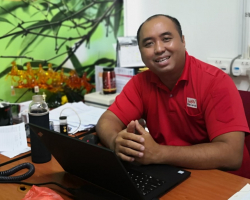
Tan, Joe

Tan, Joe
Founder & Managing Director
MSV Systems & Services Pte Ltd

Tan, Joe

Abstract
Typical semiconductor burn-in operations have multiple burn-in systems, auto-loaders & a huge quantity of burn-in boards on racks or trolleys.Limited integration between equipment had resulted in significant manual handling activities, which in turns had caused low OEE, high maintenance & high resource wastages.While many companies had attempted to automate the burn-in operations through the use of robotics & AMR, the cost of both implementation & maintenance is prohibitive. Moreover, there are little efficiency gain with these attempts & operational flexibility can be significantly compromised.This presentation showcase how a small change in the burn-in chamber design based on our patented MudaX solution, can help companies Keep It Simple, solves most, if not all the operational challenges in burn-in & Saves significant cost in burn-in operations.This presentation has very recently won the Most Inspirational Presentation award in TestConX USA conference in Arizona in May 2022.

Biography
Joe Tan is the Founder & Managing Director of MSV Systems & Services Pte Ltd established in Singapore in 2002.He graduated from the National University of Singapore with a Honours Degree in Electronics Engineering & a Master’s Degree in Industrial & System Engineering.After over 20 years of providing technical service on burn-in systems, auto-loaders & burn-in boards. MSV had invested in R&D & patented the MudaX solution to help companies Keep It Simple & Save (KISS) in burn-in operations.

Innovation Showcase
N To top
Niching Industrial Corp. Niching Industrial Corp. Dong, Rui-Xuan
Ultra low-temperature silver sintering materials for substrate-based power applications

Dong, Rui-Xuan
Project Leader
Niching Industrial Corp.

Dong, Rui-Xuan

Abstract
The demand of high powder semi-conductor devices is increasing continuously. Especially for wide band gap (WBG) semiconductors, the die-attach (DA) materials need to be bonded at a lower temperature,200 oC ideally, and operated at a high temperature (~300oC). Low-temperature sintering silver provides excellent properties to meet the requirement of DA materials on WBG applications. The common sintering temperature of commercial products is > 200dC. High sintering temperature generates a higher level of thermal stress in the DA materials, which would cause negative effects for larger dies, including void generation, delamination, crack, metallization peeling, and so on. Lower sintering temperature could reduce thermal stress during packaging processes. In addition to 200-oC sintering Ag paste (DN-1206Q), we have developed DA Ag paste with 175-oC sintering temperature (DN-1301A) for the requirement of low stress. This article is investigating the effect of sintering temperature on the performance and properties of DA materials.The storage modulus of 175oC (DN-1301A) and 200oC (DN-1206Q) sintering Ag paste are 14 and 18 GPa respectively. This is more than 20% reduction which could be a great help in terms of thermal stress. As for die shear strength (DSS), DN-1301A showed comparable results while curing at 175 oC comparing with DN-1206Q curing at 200 oC. Thermal conductivity (TC) of both 175 and 200-oC sintering Ag paste is more than 120 W/mk. In summary, lower sintering temperature can reduce the thermal stress of DA materials which is a positive contribution to the resistance of temperature variations. The performance of DN-1301A curing at 175 oC is similar to 200oC sintering Ag paste (DN-1206Q). Based on this study, it is very promising that a lower sintering temperature at 175 oC for silver sintering paste can deliver similar performance as curing at 200 oC. This could be a breakthrough for those requiring lower curing temperature such as laminate substrate-based packages.

Biography
2006-2010 Ph.D, Institute of Polymer Science and Engineering, National Taiwan University.2014-2016 Researcher, Industrial Technology Research Institute2016-2019 R&D Manager, New Micropore, Inc.2019-Now R&D Project Leader, Niching Industrial Co.

Advanced Packaging Conference
Nova Ltd Nova Ltd Szafranek, Dana
Spectral Interferometry (SI) And Vertical Traveling Scatterometry (VTS) Technology For Advanced Metrology Of Back-End-Of-Line (BEOL) Manufacturing Process Steps
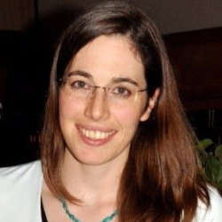
Szafranek, Dana

Szafranek, Dana
Algorithm scientist
Nova Ltd

Szafranek, Dana

Abstract
We present advances in optical critical dimension (OCD) metrology for back-end-of-line (BEOL) manufacturing process steps. Semiconductor device fabrication has advanced rapidly in recent decades, in part due to OCD metrology. Standard techniques for OCD are either spectral reflectometry and/or ellipsometry (SR/SE). We present here a new technology – Spectral Interferometry (SI)- implemented on the Nova PRISM OCD platform as a unique capability in Nova’s high-end Stand-Alone metrology solution portfolio. SI extracts unique spectral information from the sample, inaccessible by current technologies. To complement Nova PRISM, the SI data is processed with a novel algorithmic suite called Vertical Travelling Scatterometry (VTS). VTS enables selective OCD analyses of the top part of a sample separately from the bottom part of a sample within a single metrology step. Thus, it is possible to focus selectively on the topmost layers of interest to simplify the complexity of traditional OCD modeling. Multiple benefits include enhanced robustness by controlling metrology consistency under incoming variations, reduced time-to-solution due to the simplified geometry, and feasibility of modeling complex in-die applications. Recent developments in the fabrication of logic circuits and memory elements require advanced dimensional metrology steps very late in the semiconductor production process, e.g., in the back-end-of-line (BEOL) process steps where it was previously not required. Moreover, the varied topology of the samples renders metrology of the fully integrated device, i.e., metrology “in-die”, preferable, rather than using a dedicated metrology target in the scribe line. However, an “in-die” sample with many layers and buried three-dimensional architectures introduces many degrees of freedom to traditional OCD that represent the cumulative possible process variations. As a result, traditional OCD approaches based on scatterometry may not be capable of the required precision for tight process control of the BEOL process steps. It is especially beneficial to apply SI and VTS for such BEOL applications, since the separation of “relevant” and “irrelevant” information correlates to the depth of the optical signal, and thus simplifying the resulting geometric die model.

Biography
Dr. Szafranek is an algorithm developer within the semiconductor industry. Earlier in her career, she focused on computational methods for electromagnetics. In recent years, Szafranek took part in projects involving machine learning, data augmentation, feature extraction, etc., while always keeping herself minded towards the underlying fundamental physics and full physical modeling.

Innovation Showcase
P To top
PhotonDelta PhotonDelta Penning de Vries, René
Next generation microchips, powered by light
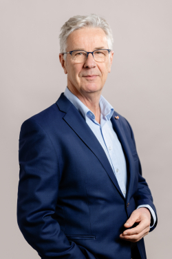
Penning de Vries, René

Penning de Vries, René
Chairman of the Supervisory Board
PhotonDelta

Penning de Vries, René

Abstract
Coming soon

Biography
Coming soon

Integrated Photonics
R To top
Robert Bosch GmbH Beer, Leopold
Semiconductors for Software Defined Vehicles
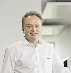
Beer, Leopold

Beer, Leopold
VP Product Management ASIC's & SOC's
Robert Bosch GmbH

Abstract
The importance of SW in Automotive is constantly increasing and currently we are reaching a point where its justified to talk about software defined vehicles.In his talk, Leopold will elaborate why semiconductors became a special focus topic for automotive OEM's and what this means for the traditional automotive semiconductor and system suppliers. At this stage of evolution, traditional, hirarchical supply chains restructure into to supply networks - opening up opportunities for new players.Based on technology requirements, Leopold will show how this new structures could look like and which are the new Key Succes Factors for the involved players.Leopold will use real life examples to explain the way Bosch Automotive Electronics addresses this topic.

Biography
Mr. Leopold BeerVP Product Management ASIC’s and SOC’s within the Bosch Automotive Electronics Division.Leopold Beer graduated the University of Stuttgart with a diploma in Physics. He specialized in semiconductor physics.Leopold started his career as engineer in the DRAM plant of Siemens Semiconductors (Today Infineon Technologies) in Regensburg and since then held various functions in the automotive and semiconductor industry.Leopold joined Bosch Sensortec in 2006 as Director of Sales and was later on promoted to Head of Global Marketing and Product Management. From 2013 to 2018 Leopold held the position of Regional President for Asia Pacific and was based in Shanghai/China. Since August 2018, Leopold oversees the ASIC & SOC product portfolio of Bosch Automotive Electronics.

Advanced Packaging Conference
S To top
Schrödinger Schrödinger Elliott, Simon
Current trends in digital chemistry to drive semiconductor innovation
Elliott, Simon

Elliott, Simon
Director - Atomic level process simulation
Schrödinger

Elliott, Simon

Abstract
The semiconductor industry is of course the enabler of digitization, but some commentators have pointed out the irony that it lags behind other industries in its own adoption of digital practices of "Industry 4.0". Looking in particular at R&D, the cost of achieving each successive technology node continues to climb steeply. With the 5 nm node estimated to cost a company $0.5bn in R&D, immense savings could be made through increased digitization of R&D activities. Such changes will be natural for today's workforce of digital natives, who access data on the cloud, share information in social networks and dial in to meetings online regardless of geography.Another aspect of the digital revolution is the transformative effect of easy access to vast computing power, and here too the semiconductor industry can benefit from its own technology. In the ideal situation, hypotheses will be tested first in simulation, as this should be both cheaper and more systematic than lab-based experiments. Looking at materials and process R&D, we discuss whether simulation software has achieved the accuracy, ease-of-use and robustness to allow this. We also focus on how to bridge gaps in expertise. Finally, we consider examples of machine learning in materials R&D and how improvements in data curation are needed right across the R&D landscape.

Biography
Co-author Dr Mathew D. Halls is Senior Vice President, Materials Science, Schrödinger.Presenting author Dr Simon Elliott is Director of atomic level process simulation at scientific software company Schrödinger, where he develops and applies techniques based on quantum mechanics and/or machine learning to the surface chemistry of deposition and etch. Prior to this, he studied chemistry at Trinity College Dublin and Karlsruhe Institute of Technology, and until 2018 led research on modelling atomic layer deposition at Ireland's Tyndall National Institute. He was co-chair of the 16th International Conference on Atomic Layer Deposition and chair of the 175-member European network on the same topic. He can sometimes be found introducing theatre improvisation games to scientists as a route to better communication skills.

Materials Innovation
Scientific Visual S.A. Scientific Visual S.A. Orlov, Ivan
Intelligent wafering: how to widen the bottleneck in semiconductor substrate manufacturing
Orlov, Ivan

Orlov, Ivan
CEO
Scientific Visual S.A.

Orlov, Ivan

Abstract
Impacted by the COVID19 pandemic and the war in Ukraine, the semiconductor market experiences unprecedented shortages. The primary bottleneck is the wafer production, which is costly and resource-intensive. As an aggravating factor, its yield is not very high: the bulk crystalline material intended for wafering is usually inspected with the human eye so that internal defects present in the ingot often end up in the finished wafers and cause their rejection. In this study, we show how to increase the wafering yield by computer-aided optimization of the wafering positions, an “intelligent wafering” method.In a typical production, semiconductor cores are extracted from an ingot with an irregular 3D shape and later sliced into wafers with a regular grid of wires. Industrial applications require wafers of standard diameters, thicknesses, and orientation, that set characteristics of the core.When internal defects are present in the core, their positioning to the cutting planes matters. Knowing the precise defect coordinates and dimensions allows calculating a core position that fits more defects into sawing gaps and, therefore, out of future wafers.We developed an “intelligent wafering” routine that computes the most optimal core position in a wafering system. It is based on digital crystal twins obtained with a TotalScan™ scanner from raw crystals. The scanner automatically detects bubbles, structures, and clouds down to 10 μm in raw crystals ranging from 0.3 kg to 350 kg. The corresponding 3D defect patterns are then analyzed using the Yield Pro v4.4 software to derive the optimal offset of the wafering grid.The method consists of the following steps:1. Scan a crystal to obtain its 3D digital twin, including internal defect morphology and spatial coordinates.2. Add orientation of crystal axis to the digital twin.3. Optimize coring positions within the crystal volume with a defined angle to a crystal axis.4. For each core, based on its defect pattern, compute an offset of the slicing grid towards the core reference that positions most of the core defects into sawing gaps.5. Adjust the position of the slicing wires to the core according to the computed offset.We will show practical examples of how intelligent wafering gets up to 7% more non-defective wafers than “blind” wafering used today. It confirms that the digitalization of crystal quality control offers tangible opportunities for processing companies to extract more quality wafers and save resources.

Biography
Dr. Ivan Orlov earned a PhD in Crystallography in Switzerland. His career embraces 20 years of R&D experience on non-destructive quality control technologies applied to optical materials and industrial crystals. He was a member of the SEMI Task Force for sapphire standard in China and collaborated with the ISO committee to establish the sapphire quality certification. Since 2010, he is leading Scientific Visual, a Swiss corporation supplying solutions for quality control of synthetic crystals.

Innovation Showcase
Scintil Photonics Scintil Photonics Langlois, Pascal
Advanced Photonic Integrated Circuits solutions with integrated lasers for ultimate optical connectivity in Datacenters, HPC and 5G
Langlois, Pascal

Langlois, Pascal
Chairman of the board
Scintil Photonics

Langlois, Pascal

Abstract
Scintil Photonics develops and markets Photonic Integrated Circuits (PICs): integrated laser arrays, multiples of 800 Gbit/sec transmitters and receivers, tunable transmitters, and receivers, as well as optical I/O for near chip and chip-chip communication). Its circuits are fabricated on a proprietary III/V-Augmented Silicon Photonics technology manufactured in a multi-customer silicon foundry. For accelerated adoption, the company also delivers the control electronics and reference package implementations. Based in Grenoble, France, and Toronto, Canada, Scintil is currently taking its innovative product to industrial level as it gears up for mass production. www.scintil-photonics.comUnique value proposition Scintil Photonics is focusing its efforts on ultra-high speed optical communication circuits for Datacenter interconnect and High-Performance Computing cloud systems. We deliver sustainable data rate, high volume production capability, while offering 40 percent power reduction.Value chain As a supplier of optical components, our circuits integrate all the optical components required to make an optical communication (lasers, modulators) We sell our circuits to equipment manufacturers in networking or high-performance computing equipment or we can sell them customers which integrate our circuits into modules. Our customers directly sell their equipment or modules to datacenters and telecom operatorsUnique technology We develop Disruptive Photonic Integrated Circuits for ultra-high-speed optical communications, exploiting a technology developed at Cea Leti. We have demonstrated high performance prototypes fabricate from our commercial foundry over the last 3 years. Some successful reliability tests were performed on our prototypes have proven reliability of the technology. SCINTIL circuit technology combines the best of III-V material and silicon photonics by molecular bonding III-V material at the backside of an already processed silicon photonic wafer. This makes us uniquely capable of integrating multiple lasers on advanced silicon photonic circuits and because one laser can carry 100 Gbit/sec and more, we can deliver ultra-high speed performances and our circuit technology leverages silicon photonic processes available in several commercial foundries. Therefore, our circuits can be supplied in volume.

Biography
Pascal LANGLOIS cofounded Scintil Photonics on November 2018 with Sylvie Menezo president and CEO. He is serving as chairman of the board. Most recently, Langlois was President and CEO of Tronics Microsystems, a Mems company he introduces in 2015 on Euronext Stock market, and which was acquired by TDK Group end of 2016. Prior to that he was Chief Sales and Marketing Officer at ST-Ericsson and from 2006, Founder of NXP and part of the executive management team responsible for global sales. He was previously with Philips Semiconductors BV, where he served in various capacities, including Senior VP of Sales and Marketing for multimarket products and VP of the automotive global market segment. He also worked with VLSI Technology, where his last position was VP for Europe, Asia Pacific and Japan operations. Pascal graduated with a Bachelor in technology from the University of Paris, and attended strategy and organization executive program from Stanford University. Langlois is also Chairman of supervisory board of Teem Photonics, an industrial laser company and Director of Yole Development, a market research firm.

Integrated Photonics
SHK Engineering and Consulting GmbH & Co. KG SHK Engineering and Consulting GmbH & Co. KG Kummer, Sebastian
No fear of high dynamics in Fab core design
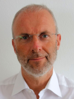
Kummer, Sebastian

Kummer, Sebastian
Chief Executive Officer
SHK Engineering and Consulting GmbH & Co. KG

Kummer, Sebastian

Abstract
The basis for planning a Fab has always been and will always be very dynamic. Changing equipment layouts and equipment configurations while a fab is being built is given fact in every Fab start-up project. New workflows and tools help to deliver good design results on time, even with this high level of dynamism. “Design competitions”, “digital twins” and the “single source of truth approach” are three success factors that will be presented with specific examples. Join this session and learn about the honest insights of Semiconductor fab core engineering and why to walk not on a beaten track became a key success factor for high quality engineering with speed and efficiency that was not thought to be possible before.

Biography
Sebastian Kummer is an engineer who designs semiconductor fab with passion. He got first insights in the semiconductor industry as Hitachi trainee in Japan. In his role as equipment engineer he was part of the first 200mm Fab start-up in Europe. Sebastian founded his own engineering and consulting firm and discovered early the power of software and electronic data to make engineering more efficient and better. He worked so far in 17 large 200mm and 300mm Frontend Fab start-up projects from construction start until after “Ready For Equipment” and in total in 33 High-Tech projects. He spent a large portion of his business life onsite in Japan, Europe, Malaysia, Taiwan and the U.S.A. and learned here about the different cultures of design, engineering and construction. In responsible roles from industrial- to facility- and hook-up engineering in projects for Siemens, Motorola, Micron, Infineon Technologies, GlobalFoundries, Nanya Technology, X-Fab and ams Osram he designed the elements inside the Fab core from automation-, equipment and subfab layouts to process laterals and hook-up. Sebastian Kummer is owner and Chief Executive Officer of SHK Engineering and Consulting. He earned his degree as graduated engineer at the University of Applied Sciences in Munich. Sebastian lives south of Munich and likes to spend his free time in the mountains. He is married and has three children.

Fab Management Forum
Silicon Austria Labs GmbH Silicon Austria Labs GmbH Roshanghias, Ali
Ultra-fine pitch Die bonding approaches with Cu interconnects for high-performance 3D IC packages
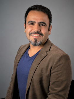
Roshanghias, Ali

Roshanghias, Ali
staff scientist
Silicon Austria Labs GmbH

Roshanghias, Ali

Abstract
Cu to Cu direct bonding is currently the most attractive approach for 3D integration due to its compatibility with the wafer back-end-of-the-line (BEOL) fabrication process. Direct or hybrid Cu bonding is an established wafer-to-wafer (w2w) bonding process at foundries. However, considering the increasing demand for heterogeneous chip stacking and high production yield with known good die (KGD), chip-to-chip (C2C), and chip-to wafer (C2W) Cu bonding processes still encounter technological challenges. In this study, we will explore different die-level bonding strategies for both protruded and recessed Cu interconnects. Here, Cu bumps with a diameter of 4 µm, and a pitch size of 18 µm surrounded by SiO2 layer were fabricated with different topographies (dishing heights) and were bonded at the different bonding temperatures. The results of the electrical examinations, bonding strength, texture, and interface analysis will be further discussed here.

Biography
Dr. Ali Roshanghias is currently a staff scientist in the department of heterogeneous integration technologies at Silicon Austria Labs (SAL). He received his Ph.D. in materials science and technology from Sharif University of Technology (Iran) in 2012. He pursued his career as a post-doc researcher at Nagaoka University of Technology (Japan) and Vienna University (Austria) in the fields of electronic materials and advanced microelectronics packaging. In 2015 he joined Silicon Austria Labs (formerly known as CTR Carinthian Tech Research AG) as a senior scientist and project manager. His research interests include heterogeneous integration technologies, hybrid electronics, and 3D integration.

Advanced Packaging Conference
Soitec Soitec Maleville, Christophe
Industry talk
Maleville, Christophe

Maleville, Christophe
CTO, Executive VP Innovation Organization
Soitec

Maleville, Christophe

Abstract
Coming Soon

Biography
Christophe Maleville has been appointed senior vice president of Soitec's Innovation.He joined Soitec in 1993 and was a driving force behind the company's joint research activities with CEA-Leti. For several years, he led new SOI process development, oversaw SOI technology transfer from R&D to production, and managed customer certifications. He also served as vice president, SOI Products Platform at Soitec, working closely with key customers worldwide. Maleville has authored or co-authored more than 30 papers and also holds some 30 patents. He has a PhD in microelectronics from Grenoble Institute of Technology and obtained an executive MBA from INSEAD.

ITF Beyond 5G
ST Microelectronics ST Microelectronics Theveniau, Raphael
Complete LVS verification methodology and process for complex System-In-Package assemblies
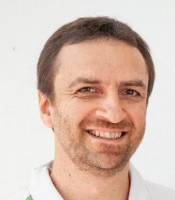
Theveniau, Raphael

Theveniau, Raphael
CAD Support Senior Staff Engineer
ST Microelectronics

Theveniau, Raphael

Abstract
Systems in Package (SiP) have been around for some years and were typically the integration of multiple bare unpackaged chips along with discrete devices interconnected with just a few signals. However, as silicon scaling (aka Moore’s Law) slows and silicon densities reach their physical limits, there is growing shift to disaggregation of once monolithic functions into smaller, node optimized high yield chiplets, heterogeneously integrated on a high-performance substrate as an advanced System-In-Package (SiP), or module. These designs utilize multiple high performance and high bandwidth interfaces between the chiplets enabling higher densities, greater device functionality, and improved overall silicon yield. All the devices used in a SiP are often designed concurrently, by different teams, in different time zones. Thus, the risk to make mistakes in data exchange is very high. To mitigate this risk a comprehensive system description along with a controlled data exchange flow is key. Furthermore, although each device is tested independently, there is a need for a formal signoff check or verification that covers the whole system.In STMicroelectronics we have developed an automated layout versus schematic (LVS) methodology that electrically verifies the module and system-level designs logical connectivity. Using a combined 3D assembly level DRC/LVS methodology our divisions can prevent System in Package failures due to swapped balls, shorted power nets or any uncontrolled change in the design layouts.This paper will describe the essential steps and process of a fully integrated workflow that can verify and validate a complete multi-chiplet SiP design assembly using an LVS approach including the technologies used to enable such a solution.

Biography
After 5 years spent in Cadence UK and 5 years in Texas Instruments France, Raphael Theveniau joined STMicroelectronics in 2009 as System in Package expert. He is now part of Technology R&D group in ST, in Digital Design Flows and Methodology team. He has more than 20 years of experience in Digital Design, covering most aspects of place and route and signoff flows and package design. His role as SiP expert consists in developing, promoting and supporting flows through ST kits for internal divisions as as well as external customers. Now his role is more focused on Die-Package Co-design flows, and more specifically System in Package LVS.

Advanced Packaging Conference
SYSTEMA SYSTEMA Roßbach, Philipp
How to simplify engineers’ life in complex Semiconductor Manufacturing. About democratization of information and its usage in production scheduling and root cause analysis.
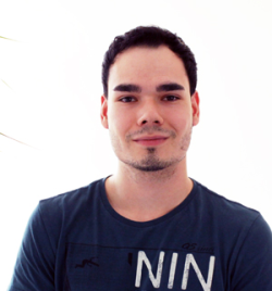
Roßbach, Philipp

Roßbach, Philipp

SYSTEMA

Roßbach, Philipp

Abstract
Digitalization keeps driving increased demand for microchips. Shortening the product lifecycle and the high variety of customer-specific devices lead to a growing need for high-mix low-volume (HMLV) semiconductor production. SYSTEMA drives several activities to achieve a novel quality in production control and explainability of how the fab behaves. The “Autonomous Integrated Scheduling for Semiconductor Industry” (AISSI) project partners with Bosch, Nexperia, Simlab, KIT. Goal is to apply AI-based methods to enable autonomous production scheduling. However, such AI-solutions are “black boxes”. They will only be accepted, if users understand the system: “explainability”– see also the EU "General Data Protection Regulation GDPR".Objective is simplifying engineer’s work and hand-over a powerful framework for continuous and rapid learning - and maybe creatig a smile.SYSTEMA created a semantically inspired holistic information model (HIM). This offers, for the first time, an easily understandable access and method to close the gap between huge amount of data and the need to analyze this data in real-time, while offering at the same time the possibility to create formerly unseen, personalized “insights”. The solution concept implements a single point of truth (SPOT) approach, enabling best algorithmic efficiency at the same time. Complex WHAT-IF-Analysis is enabled:- What are the root causes of those dynamically appearing “WIP bubbles”- Did the efficiency of the entire production line sustainably improved when the new scheduling method was introduced?Additionally, counter-factual analysis is enabled – which is critical to enable human learning. The aim is to create an informational 'play space' that is fundamental to human imagination.AI-based methodologies seem to provide important capabilities in order to solve the complex planning task of production or the "job scheduling problem". SYSTEMA has analyzed the requirements together with Nexperia and created a new AI-based scheduling concept utilizing 4M-methodology. Detailed analysis accomplished are, e.g., setup- and occupancy planning of batching machines (furnaces), maintenance and shift activities and many others.Examples highlighted during poster session and presentation will touch a “counterfactual” improvement of an entire production area (such as furnace) and showing its influence on the entire fab;a dive-in into an integrated AI-based scheduling method.

Biography
Philipp Roßbach (Speaker)holds a M.Sc. in Applied Informatics – Data Science from HTW Dresden, University Applied Science (Germany). He started in 2015 at SYSTEMA for his B.Sc., and later during his M.Sc., and supported his first projects for semiconductor manufacturing. Currently, he is 1) contributing to the R&D program AISSI at SYSTEMA while 2) also researching at HTW for Cell-based analysis in systems medicine.For AISSI, (“Autonomous Integrated Scheduling for Semiconductor Industry”) Philipp helps to develop, integrate and apply novel AI-based approaches in semiconductor manufacturing that builds on European quality-thinking from the automotive sector.For HTW, his fields of research are data-driven modeling for the analysis of multicellular tissue organization and model-based prediction of an Effective Adhesion Parameter guiding multi-type cell segregation.Dr. Gerhard Luhn (Mentor)holds a Ph.D in engineering science from the University of Erlangen-Nuremberg (Germany). He has more than 25 years of experience in semiconductor manufacturing and information science. Currently, he is heading an innovation program at SYSTEMA GmbH together with the Technical University of Dresden and several major renowned industry partners, which aims at the industrial proof, prototypical and scientific validation of a new, mathematically grounded method of causal-holistic information processing. Gerhard previously worked as team leader / program manager and research fellow for Infineon/Dresden, Technical University Dresden and Siemens/Munich. He also held various positions in France with Siemens / IBM joint venture in Essonnes; and ST Microelectronics in Crolles. Gerhard holds a patent application, authors scientific papers, and engages in the science of information.

Fab Management Forum
T To top
TechInsights Inc. TechInsights Inc. Hutcheson, Dan
Market Trends
Hutcheson, Dan

Hutcheson, Dan
Vice Chair
TechInsights Inc.

Hutcheson, Dan

Abstract
Coming soon

Biography
Dan is Vice Chair of TechInsights Inc. He is a recognized authority on the semiconductor industry, winning SEMI’s Sales and Marketing Excellence Award<sup>[1]</sup> in 2012 for “empowering executives with tremendous strategic and tactical marketing value" through his e-letter, The Chip Insider®; his book Maxims of Hi-Tech, and his many interviews of executives. As some industry leaders have said, “He is the marketing voice and expert for the industry.” “Dan has methodically captured the essence of the industry and produced it in such a way for all to benefit … He has been such an integral part of the industry for so long, it is difficult to imagine the industry without his contributions.” Dan’s public work on the industry has often focused on challenging predictions of the demise of Moore’s Law that date back decades by demonstrating how doomsayers have been outpaced by emergent behavior through the innate ability of technologists to innovate. This has included invited articles for Scientific American, the SIA, and the Plenary at the SPIE Advanced Lithography Conference.[1] Formerly SEMI’s Bob Graham Award

Fab Management Forum
Technical University of Applied Sciences Regensburg Ramsauer, Ralf
Jailhouse: Mixed Criticality Systems for Semicondutor Manufacturing

Ramsauer, Ralf
Head of Research Group
Technical University of Applied Sciences Regensburg

Abstract
The advent of multi-core CPUs in nearly all embedded markets has prompted an architectural trend towards combining safety critical and uncritical software on single hardware units. We present an architecture for mixed-criticality systems based on Linux that allows for the consolidation critical and uncritical parts onto a single hardware unit. In the context of the iDev 4.0 project, the use-case of this technological building block is to reduce the overall amount of distributed computational hardware components accross semiconductor assembly lines in fabs. CPU virtualisation extensions enable strict and static partitioning of hardware by direct assignment of resources, which allows us to boot additional operating systems or bare metal applications running aside Linux. The hypervisor Jailhouse is at the core of the architecture and ensures that the resulting domains may serve workloads of different criticality and can not interfere in an unintended way. This retains Linux's feature-richness in uncritical parts, while frugal safety and real-time critical applications execute in isolated domains. Architectural simplicity is a central aspect of our approach and a precondition for reliable implementability and successful certification. In this work, we present our envisioned base system architecture, and elaborate implications on the transition from existing legacy systems to a consolidated environment.

Biography
Ralf Ramsauer is a postdoctoral researcher at the Technical University of Applied Sciences Regensburg where he leads the Systems Architecture Research Group. His academic research interest focuses on mixed- and safety-critical systems, real-time embedded systems and embedded virtualisation on various architectures. This covers the full software stack of embedded systems, from hardware-related low-level virtualisation technologies via kernel-space up to userland. Ralf is a codeveloper of the Linux-based statically partitioning hypervisor Jailhouse, where he currently works on the RISC-V port.

Fab Management Forum
TERADYNE TERADYNE Ducrocq, David
Minimizing Execution Risk in Test Solution Development Projects with a Technical Project Lead
Ducrocq, David

Ducrocq, David
Application Test Technical Leader
TERADYNE

Ducrocq, David

Abstract
Test development projects are a mix of engineering disciplines spanning PCB design and layout, software engineering, measurement technology, test system configuration and test cell setup, a complex and interdependent ecosystem. A project manager, who is primarily focused on schedule, is unable to oversee the many disciplines and adequately assess technical risks in each area and across the entire project. This inability to assess risks and their impact on the entire project is often the root cause of catastrophic project failures and missed delivery schedules. By including a technical project lead in the project, there is a single point of responsibility for assessing technical risk across the project, developing mitigation plans and driving countermeasures to completion.This paper will address:1. The role the technical project lead plays with each stakeholder in the project and to the project as a whole, including:1.1 solution architecture1.2 resource identification and allocation1.3 technical execution of the project1.4 issue mitigation and resolution1.5 communications with both internal and external stakeholders2. Qualifications of a technical project lead3. An overview of the risk assessment and mitigation process4. Expected benefits to the project, team and working environment

Biography
David Ducrocq is an Application Project Leader at Teradyne, where he focuses on PMIC and Image Sensor Test program development and is a specialist on Teradyne’s FLEX, MicroFLEX and UltraFLEX test systems. David has played a leading role in defining and implementing Teradyne’s technical project lead program across the organization. David joined Teradyne in 1999 as an Applications Engineer for the Test Assistance Group in Grenoble/France, where he worked on Catalyst on RF Devices.David studied Electrical Engineering and Computer Science at the Institute de Recherche et d'Enseignement Superieur aux Techniques de l'Electronique* (IRESTE), Université´ de Nantes, France.After graduation, David worked in the field of Image Processing for 2 years. He then worked as a subcontractor for Teradyne for 4 years on the A3xx, A5xx and Catalyst test systems.In 1999, David joined the Test Assistance Group at Teradyne in Grenoble/France as an Applications Engineer. David worked on Catalyst on RF Devices and is now a specialist on FLEX/MicroFlex/UltraFlex test systems.From 2012, David took the responsibility of several key customers as an Application Project Leader mainly focusing on PMIC and Image Sensor Test program development. During this period, David played a leading role in definition and implementation of the technical project lead and was in charge of its roll-out throughout the corporation.*Institute of Research and Higher Education for the Techniques of Electronics

Innovation Showcase
Texas Instruments Texas Instruments Thomas, Vipin Koshy
Machine Learning for Automated Image Classification in Yield Enhancement
Thomas, Vipin Koshy

Thomas, Vipin Koshy
Intern
Texas Instruments

Thomas, Vipin Koshy

Abstract
One of the most repetitive and time-consuming tasks for our operation specialists in the Yield Enhancement group is the manual image classification. Moreover, due to stress and environmental conditions the consistency and accuracy of the manual classification varies. Therefore, we have been looking for a fully automated solution to relieve our specialists from the tedious classification tasks. In addition, the implementation of the solution to our production flow and integration to our fab automation has a positive impact on productivity.We have explored various options available for out pilot automated classification project and found Convolutional Neural Networks (CNN) can produce consistent and accurate results for one specific classification task. We use a generally accepted CNN classification model trained on thousands of images from the scanning electron microscope. Since the input image dataset was highly biased, we used Image augmentation techniques to improve the results. In addition, we have also considered techniques like Transfer Learning to scale our solution to other image classification tasks. Our current model outperforms in terms of consistency and accuracy when compared to the manual classification.We will achieve more by integrating fab automation to the automated image classification. A successful completion of the classification tasks triggers the fab automation to check whether to logout the lot, to inspect more wafer from the same lot or to put the lot on hold. With a fully automated fab process, we can minimize delays and waiting times of wafers. So far, we have been successful in implementing and integrating automated image classification with fab automation as a pilot project. We have identified a high fan out potential of this automated classification method and will be working to transfer the promising results to other areas as well.

Biography
Vipin holds a bachelor degree in Computer Science and Engineering from Mahatma Gandhi University, India (2013). He has worked for about 4 years in various companies (2014 - 2019) and gained knowledge on diverse technologies and frameworks such as mainframes, angular framework, data analysis with Python, cloud and Data Science/ML frameworks. Since Oct 2020, he is pursuing a MSc. Applied Computer Science at TH Deggendorf with expected graduation in Apr 2023. Currently, he is working at Texas Instruments as an Intern (Mar 2022 - Aug 2022). He is interested in Data Science projects and Edge AI.

Fab Management Forum
time:matters GmbH time:matters GmbH Kohnen, Alexander
Panel Discussion – Navigating through global developments affecting the supply chain management
Kohnen, Alexander

Kohnen, Alexander
CEO
time:matters GmbH

Kohnen, Alexander

Abstract
10:30 - Panel Discussion – Navigating through global developments affecting the supply chain management How can we enable improvements in supply chain?Supply chain changes / access to x (materials, tools, etc e.g. lead time to tools) / Supply chain management post covid / new relationships / how can we help our suppliers to faster deliveryhow to scale material supply/capacity exponentiallyGlobal development on supply-customer relationship based on covid-era lessons learntTool usage beyond expectancy (legacy tools) in fabs, what will it happen in these technologies in a few years (sustainability aspect)? Moderator: Dan Hutchinson, CEO and Chairman, VLSI

Biography
Alexander Kohnen is CEO and Managing Director Strategy and Sales for time:matters Holding GmbH in Neu-Isenburg. As an expert in high-performance and worldwide special speed logistics and in time-critical international spare parts logistics, time:matters provides tailor-made and fast solutions for particularly urgent and complex logistical tasks. Besides speed and reliability, providing an individual, flexible service is paramount.Alexander Kohnen began his career in 2000 as Information Manager Sales & Marketing with Lufthansa Cargo AG in Frankfurt am Main. In his 17 years with Lufthansa Cargo, he gained extensive management experience in various leadership roles at home and abroad, including a period from 2008 as Country Manager Sales and Handling Benelux in Amsterdam. He moved to Stockholm in 2011 to take up the role of Director Sales and Handling Nordics & Baltics, covering sales, marketing and commercial management in Scandinavia. Before his switch to time:matters, he was most recently Senior Director with responsibility for the Industry Development & Product Management division at Lufthansa Cargo in Frankfurt.In November 2017, Alexander Kohnen joined the management team at time:matters. The company finished that same year with a 55% year-on-year increase in revenue and registered tremendous growth in the automotive and high-tech/semicon focus industries. Under Alexander Kohnen’s leadership, time:matters has added another 17 stations (Tel Aviv, Mexico and 15 stations in the US) to its unique Sameday Air network for same-day transports. The logistics company has also been awarded ISO 14001:2015 environmental management certification. By acquiring CB Customs Broker and Customs Broker Cargo Handling, time:matters has been able to extensively expand its customs clearance and handling portfolio. In the coming year, with Alexander Kohnen at its helm, the company is again planning countless internationalization projects, further digitization of its offering, connection of customer and partner systems via APIs and further development of its time:matters airmates On Board Courier platform.time:matters is now considered one of the leading providers of flexible special speed solutions. The internationally renowned logistics specialist has already been operating extremely successfully in the sector since 2002, which has been continuously reflected in its positive revenue trend. In 2017 time:matters concluded with 108 million euros in revenue.The native of Cologne trained as a commercial air transport apprentice with Lufthansa AG in Frankfurt, before going on to complete a Business Administration degree. Alexander Kohnen is married and has three children.

Fab Management Forum
Trinity College Dublin Boland, John
Nanoscale metals are comprised of grain boundaries that are significantly different from those found in bulk materials
Boland, John

Boland, John
Professor of Chemistry
Trinity College Dublin

Abstract
Metals are the simplest of solids and copper is probably the best known and most studied of all. The properties of copper metal of macroscopic dimension are well understood. However, the same cannot said when copper is reduced to nanoscale dimensions. Like most metals, copper is a granular solid comprised of grains with boundaries between them. Here in this talk we focus on what we have learned about nanoscale copper by using scanning tunneling microscopy and molecular static simulations. In particular we visualize for the first time the 3D structure of grain boundaries (GBs) that emerge at the surface of nearly coplanar copper nanocrystalline (111) films. Remarkably, we find that GBs at surfaces are different from those in the bulk. We show that GBs in metals actually prefer to lie along close packed planes which in turn necessitates the tilting and restructuring of the boundary as it approaches the (111) surface. The restructuring depth can be a few to several tens of nanometers. This behavior is due to a previously unrecognized phenomenon that involves the rotation of the dislocation lines that comprise the GB, which minimize the energy and has significant implications for materials properties [1, 2]. Since transport in copper occurs predominantly along close packed planes these restructure boundaries, which also lie along close packed planes, are expected to have unusual scattering properties. Whether fully relaxed restructured boundaries are possible under device fabrication conditions remains to be established.References:[1] Xiaopu Zhang, Jian Han, Adrian P. Sutton, David J. Srolovitz, John J. Boland. Science 357, 397-400 (2017)[2] Xiaopu Zhang, Hailong Wang, Moneesch Upmanyu, John J. Boland (under review)

Biography
Prof John Boland received a BSc degree in chemistry from University College Dublin and a PhD in chemical physics from the California Institute of Technology, where he was an IBM graduate fellow and recipient of the Newby-McKoy graduate research award. From 1984 to 1994 Prof Boland was a member of the research staff at the IBM T.J. Watson Research Center (New York). In 1994 he joined the chemistry faculty at the University of North Carolina at Chapel Hill where he was appointed the J.J. Hermans Chair Professor of Chemistry and Applied and Materials Science. In 2002 Prof Boland moved to the School of Chemistry at Trinity College Dublin as a Science Foundation Ireland Principal Investigator and Professor of Chemistry. In June 2005 he was appointed Director of the Centre for Research on Adaptive Nanostructures and Nanodevices (CRANN) until July 2013. He also served as TCD Vice President and Dean of Research (2015-2017).Prof. Boland became an elected Fellow of Trinity College Dublin in 2008, a fellow of the American Vacuum Society (AVS) in 2009 and a fellow of the American Association for the Advancement of Science (AAAS) in 2010. He was the 2011 laureate of the ACSIN prize for nanoscience. He is the recipient of an Outstanding Researcher Awards from IBM (1992) and Intel (2017). He is the recipient of a prestigious European Research Council Advanced Grant. Prof. Boland’s research interests are focussed on the novel properties of nanoscale materials and their potential in device and sensor applications.

Materials Innovation
Tyndall National Institute Tyndall National Institute Ghosh, Samir
Heterogeneously integrated InP-laser on Silicon Photonics realized by micro-transfer printing

Ghosh, Samir

Ghosh, Samir
Researcher
Tyndall National Institute

Ghosh, Samir

Abstract
Silicon photonics have gained immense commercial interest in data-center market and soon it will enter other domains as well including biomedical, space applications and so on. Silicon being an indirect bandgap semiconductor efficient lasing cannot be achieved. Therefore, hybrid or heterogeneous integration techniques are normally used to incorporate laser with silicon photonics (SiP) platform. These techniques of integrating lasers on SiP platform are far from ideal in-terms of volume, cost and yield. Micro-transfer printing is an emerging technology which enables massively parallel integration with high yield and hence bring the cost down. In this talk transfer printing of InP-based laser on SiP chip will be presented.

Biography
Samir Ghosh obtained his Ph.D. degree in Photonics Engineering from Ghent University, Gent, Belgium in 2013. Afterwards he worked at various academic institutes as a postdoctoral researcher including McGill University – Canada, University of California - Davis, The University of Tokyo - Japan, and Nanyang Technological University - Singapore. Since October, 2020 he is working as a researcher at Tyndall National Institute, Cork, Ireland where his primary interest lies on heterogeneous integration of InP, LN-based devices on Si-Photonics platform utilizing micro-transfer printing technology. His has (co-) authored of 30 publications in referred journals and in international conference proceedings. His broad research interests include large-scale photonic integrated circuit for communication, sensing and imaging applications.

Integrated Photonics
W To top
Wooptix Wooptix Gaudestad, Jan
New Metrology Technique for Measuring Patterned Wafer Geometry on a full 300mm wafer
Gaudestad, Jan

Gaudestad, Jan
VP Business Development
Wooptix

Gaudestad, Jan

Abstract
The flatness of the silicon wafers used to manufacture integrated circuits (IC) is controlled to tight tolerances to help ensure that the full wafer is sufficiently flat for lithographic processing. Chemical-Mechanical Planarization (CMP) is one of many processes outside the lithographic sector that will influence wafer flatness across each image lithographic exposure section field and across the wafer. Advanced lithographic patterning processes require a detailed map of the wafer shape to avoid overlay errors caused by depth-of-focus issues. In recent years, a metrology tool named PWG5TM (Patterned Wafer Geometry, 5th generation), based on using double Fizeau interferometry to generate phase changes from the interferometric pattern applied to the reflective surface, has been used to generate a wafer geometry map to correct for process induced focus issues as well as overlay problems. In this paper we present Wave Front Phase Imaging (WFPI); a new patterned wafer geometry technique that measures the wave front phase utilizing two intensity images of the light reflected off the patterned wafer. We show that the 300mm machine acquires 7.65 million data points in 5 seconds on the full 300mm patterned wafer with a lateral resolution of 96µm. For the semiconductor industry to uphold Moore’s Law, among the key challenges are the ever-tightening overlay requirements. In the latest immersion scanners that perform at the sub-2 nm overlay level, the overlay budget becomes more and more determined by process-induced overlay errors from fab steps such as etching, thin film deposition, Chemical-Mechanical Planarization (CMP) and thermal anneal. All these processing steps can introduce stress, or stress changes, in the thin films on top of the silicon wafers that again can result in significant wafer distortions. Since the data acquisition time of Wave Front Phase Imaging (WPFI) is mainly controlled by the shutter speed of the camera when used in a dual camera set up, which is generally set to less than a second, in addition to very high data count, it makes WPFI a strong alternative technique for measuring and correcting for process induced stress quickly. Adding that WFPI is highly resistant to vibrations in addition to having large tolerances to wafer placements in the optical measurement cavity, makes WFPI a viable solution in a high-volume device manufacturing fab setting.

Biography
Jan Gaudestad is San Francisco based VP of Business Development for Wooptix, a small VC funded Intel Capital portfolio company, that is developing metrology equipment for the semiconductor fab market. He also serves on the board of directors for Elevate Semiconductors, a fables semiconductor company based in San Diego California. He has more than 20 years of experience in the semiconductor industry. He worked on strategic accounts at InvenSense/TDK for consumer level MEMS motion sensors. He spent 14 years at Neocera, an Intel Capital funded backend semiconductor equipment company managing product development, global sales, applications, and new business development. He also spent time working on emerging technologies for virtual and augmented reality applications. He received his MBA from Santa Clara University in 2009. He earned a master’s degree in Physics in 2001 from University of Maryland, College Park, and a master’s degree in Physics in 2000 from the Norwegian University of Science and Technology in Trondheim, Norway.

Innovation Showcase
X To top
X-fab X-fab U’Ren, Gregory
Industry talk
U’Ren, Gregory

U’Ren, Gregory
Director RF Technologies X-FAB Group
X-fab

U’Ren, Gregory

Abstract
Coming Soon

Biography
Dr. Gregory U’Ren is the Director of RF Technologies at X-FAB responsible for incubating and subsequently delivering integrated device technology solutions including reference designs and foundational design IP. During his career, he has held both leadership and individual roles contributing to the advancement of a broad range of specialty technologies including SiGe BiCMOS, RF-SOI, MEMS, and GaN. Current activities are focused on the RF front end for 5G or 6G systems engaging various collaborations with academic and industrial partners on a wide range of topics including materials, process, RF/mmW characterization, advanced modeling, and EDA tooling enhancements to support several program initiatives at X-FAB.He is a senior member of IEEE, a member of the American Physics Society, and holds over 30 patents. He completed his PhD and MS at the University of California Los Angeles.

ITF Beyond 5G
X-fab X-fab Tillner, Rico
How medical devices are changing the customer-foundry relationship
Tillner, Rico

Tillner, Rico
CEO
X-fab

Tillner, Rico

Abstract
Over the last years the medical industry was pushing for more automation to improve time to result and cost. The Covid pandemic has given another push in this direction.Automotive driven foundries are the perfect partner for the medical industry as they are used to long qualification times and even longer product lifecycles which are also needed in the medical business. Medical and life science applications also require functionalities which cannot be bought out of the shelf. Designer and foundry partners need to develop a close partnership to create a successful product for these markets.Life science companies like MaxWell Biosystems are designing such unique chips for very dedicated use cases. The CMOS-based microelectrode arrays of MaxWell Biosystems are integrating 26’400 platinum microelectrodes in an array, using a MEMS process. These electrodes are used to pick-up the minute signals of neurons, cultured directly on top of the microelectrode array. Together with the use of induced pluripotent stem cells this enables an unprecedented access to human disease models in a dish for drug discovery in the pharmaceutical industry, increasing the potential success of new medicines for neurodegenerative diseases.X-FAB as pure play foundry has developed unique skills to support customers like MaxWell Biosystems, no matter if they are startup companies or big players in their markets.

Biography
Rico Tillner has 15 years of experience in the semiconductor industry. After his master’s degree in electrical engineering at Technical University Dresden he started his career at X-FAB Dresden. From 2007 until 2015 he worked as Process integration engineer, responsible for a 0.6µm automotive mixed signal technology. During that time, he gathered experience in quality methods, yield improvement projects and the conversion from a 6-inch to an 8-inch production. In 2016 he becomes the quality manager of X-Fab Dresden. Since 2018 Rico Tillner is the site manager and CEO of X-FAB in Dresden. Co-presenter Urs FreyUrs Frey received the diploma in electrical engineering from ETH Zurich, Switzerland, in 2003 and the Ph.D. degree for his work on high-density neural interfaces and microhotplate gas sensors from the Physical Electronics Laboratory, ETH Zurich, in 2008. From 2009 to 2010, he was with IBM Research Zurich, Switzerland, where he worked on mixed-signal circuit design for non-volatile memory devices. In 2011 he joined the RIKEN Quantitative Biology Center in Kobe, Japan, where he was heading an independent laboratory focusing on CMOS-based bioelectronics and biosensors. In 2016, he co-founded MaxWell Biosystems AG in Switzerland, where he is currently the CEO.

Fab Management Forum
X-FAB Group X-FAB Group Schoder, Henryk
The people challenge: How to overcome the skill shortage in the FAB´s?
Schoder, Henryk

Schoder, Henryk
Vice President Human Resources
X-FAB Group

Schoder, Henryk

Abstract
In the light of Europe’s ambition to reinforce the semiconductor ecosystem in the EU with announcement of the Chips Act and significant planned investments into the semiconductor industry, the key to success has be and will be the ability to attract and keep the people required to run a fab. On the level of technicians we already see a substantial shortage in skills and people, and with the new stimulation package that shortage will become a major obstacle for growth ambition in the industry. The presentation will cover some important initiatives and ideas to tackle the problems particular in the are of Manufacturing.

Biography
Since 2014, Henryk Schoder has been overseeing the global HR activities for the X-FAB Group as VP Human Resources. Prior to joining X-FAB, Henryk was HR & IT Manager at Masdar’s solar manufacturing plant in Germany. Before that he worked as Senior Consultant and Managing director for the MRL Consulting Group in the UK, Singapore and Dubai. He started his career as recruiting manager at Infineon. Henryk holds a Master degree in Psychology from the University of Jena, Germany.

Fab Management Forum