4 To top
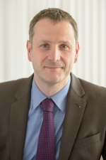
4GENE GmbH 4GENE GmbH Adamski, Heimo
Biotechnology meets Industry - Today: Overheating Alert Solution
Adamski, Heimo

Adamski, Heimo
CEO
4GENE GmbH

Adamski, Heimo

Abstract
4GENE´s innovative, biotechnological process allows for the production of a new form of sugar-bound odors (namely glucosides) as they naturally occur in crop plants. They can be released from their bound form by different triggers, such as heat. The possibility to realease a previously bound and non-volatile odor due to heat means, that the odor can be used as a warning signal in technical applications.When placed onto technical devices like cables, tubing or printed circuits in the form of small labels as a carrier for the bound odor, they become pyrolysed in case of overheating and the released odor signature acts as the warning signal for overheating (>80–130°C) – the odor is “turned on”. When temperature isn’t in the critical zone, the odor is likewise “turned off”.For this warning signal application, an odor that is uncommon in the surrounding of a technical installation but not awkward should be selected, and the odor should be removable by air conditioning. 4GENE offers 4 different odors or a mix of those for such use.The major benefit of our solution is that you will be given enough lead time before something actually happens (e.g. fire) to shut down the machine or the device in question. This enables you to not only prevent the fire from starting but also it prevents financial damage and a shutdown of the damaged machine. Further more it helps to protect yourself, your family or in a corporate environment protect your employees. Compared to traditional solutions, the 4GENE flavor-on-demand technology does not use any hardware and therefore cannot fail. There is no equivalent or comparable solution available on the market today.4GENE does not produce any pollution and we use green energy whenever possible during production.

Biography
Heimo AdamskiState-certified Business Information Manager with over 35 years of experience in international sales & marketing in corporations and start-ups.

Young Disruptors
A To top
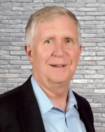
ABB Semiconductors ABB Semiconductors Kraxenberger, Manfred
Kraxenberger, Manfred

Kraxenberger, Manfred
Vice President
ABB Semiconductors

Kraxenberger, Manfred

Biography
Manfred Kraxenberger is currently factory manager for ABB’s BiMOS wafer fab and assembly line in Lenzburg, Switzerland.Manfred Kraxenberger studied physical engineering and started working as process engineer at Siemens Semiconductor in Munich in 1986. Over the last 30 years, he has held several engineering and management positions in manufacturing as well as R&D at Siemens/Infineon/Qimonda and Globalfoundries.

Fab Management Forum
Advacam Ltd Advacam Ltd Kalliopuska, Juha
Spectral Imaging Cameras with Application Examples
Kalliopuska, Juha

Kalliopuska, Juha
CEO, Co-Founder
Advacam Ltd

Kalliopuska, Juha

Abstract
ADVACAM has been able to successfully commercialize photon counting technology developed at CERN’s Medipix collaboration. ADVACAM utilizes different Medipix readout chips, namely Timepix, Medipix3 and Timepix3, for spectral imaging of X-ray and gamma radiation. Each readout possesses different properties suitable for different applications. Presentation introduces the photon counting technology and gives several application examples. The multi threshold spectral X-ray imaging in non-destructive testing (NDT) enables material discrimination that is used in radiography, computed tomography and high speed conveyer belt or robotic scanning applications. The fully spectral X-ray imaging in the NDT enables subpixel resolution down to 9 um resolution without need of geometric magnification. The energy dispersive X-ray diffraction (XRD) using the fully spectral X-ray detector speeds up the sample analysis by a factor of 100 using a simple polychromatic XRD setup without moving parts. Finally the fully spectral radiation imaging detector enables a lightweight single layer compton cameras for identification radiation sources and their location. The applications of the compton camera are found in medical imaging, nuclear safety and security.

Biography
Dr. Juha Kalliopuska, Chief Executive Officer, Co-founder of ADVACAM Oy. ADVACAM Oy, established in 2012, is a one-stop shop for radiation detector manufacturing and micropackaging services. Juha has extensive knowledge in silicon sensor manufacturing and has worked to develop the core edgeless sensor building block for the hybrid sensors that allows scalability of the detector area of ADVACAM's camera products. Juha has long-term experience in customer relationship and sales development, starting in his previous job at VTT Technical Research Centre of Finland from 2003-2013.

Finnish Special Session
AdvancedEPI AdvancedEPI Colston, Gerard
Novel Group IV Epitaxial Materials
Colston, Gerard

Colston, Gerard
Managing Director and founder
AdvancedEPI

Colston, Gerard

Abstract
Advanced Epi supplies and can develop processes for all Group IV semiconductors with capabilities across epitaxial growth, in-depth material characterisation and device fabrication. This talk will cover a number of different materials, their properties and applications from Group IV, focussing primarily on cubic silicon carbide (3C-SiC) and germanium tin (GeSn) alloys which can both be grown on silicon wafers and integrated into silicon processing. These novel materials each have the capability to revolutionise the field of semiconductors across power electronics, sensing, light emission and mobile communications to name but a few.

Biography
Dr Gerard Colston is the Managing Director and founder of Advanced Epi Materials and Devices Ltd a UK based company offering epitaxial services across Group IV semiconductors. Dr Colston completed his PhD in cubic silicon carbide growth technology and has researched other semiconductor materials including various Si alloys, Ge, GeSn and SiC throughout his professional and academic career.

Exhibitor Presentations
Alertgy Alertgy Hubert, John
Non-Invasive Continuous Glucose Monitor (NICGM) for Diabetics

Hubert, John

Hubert, John
VP of Engineering for Alertgy
Alertgy

Hubert, John

Abstract
Alertgy is developing the first noninvasive continuous glucose monitor (NICGM) wristband. The monitor consists of a wristband, App and IoT solution. Using its proprietary technology, Alertgy’s Freedom detects blood glucose levels without any invasive needles or sensors, and alerts the patient and family, friends and caregivers via its smartphone link and automated alarm capability. These features provide accurate routine blood glucose measurements without the customary needle prick and meter device or implanted sensor needles and provide potentially lifesaving alerts when glucose levels are dangerously high or low. Historical data can be reviewed by the patient or shared with healthcare professionals.

Biography
John Hubert, VP Engineering of Alertgy has designed over 200 Monolithic Microwave Integrated Circuits helping to provide a paradigm shift that significantly reduced the size of military and commercial products. Lockheed Martin awarded him the coveted “APEX” award after his team successfully developed a MMIC based High-Power Quasi-Optic Microwave Amplifier for DARPA. John also participated in spinning out a startup commercial company from Lockheed Martin, producing MMIC based transceivers and radiometers. Throughout his career, he has co-authored several papers, patents as well as a textbook. John earned an accelerated MS degree in Electrical and Computer Engineering from UMass through an industry sponsored program.

SMART MedTech
Amazon Web Services Amazon Web Services Pellerin, David
Cloud-Accelerated Innovation for Semiconductor Design and Verification
Pellerin, David

Pellerin, David
Head of WW Business Development, Hitech/Semiconductor
Amazon Web Services

Pellerin, David

Abstract
An explosion in the number and variety of intelligent edge devices, combined with cloud computing, are driving a need for more rapid innovation in semiconductor products. This talk presents examples and best-practices for cloud-accelerated semiconductor design and verification, including use-cases and examples inside and outside of Amazon. The talk will include an overview of how the development of next-generation products is enhanced through the use of cloud for scalable, high-throughput EDA flows. The talk will cover performance optimizations for computing, storage, and EDA workload orchestration, as well as covering how cloud enables secure collaboration in the semiconductor and electronics supply chain.

Biography
David Pellerin serves as Head of Worldwide Business Development for Hitech/Semiconductor at Amazon Web Services. Prior to joining AWS, Mr. Pellerin had a career in electronic design automation and hardware-accelerated reconfigurable computing. He has experience with digital logic simulation and optimization, high-level synthesis, grid and cluster computing, and embedded systems for image, video, and network processing. He has published five Prentice Hall technical books on EDA-related topics.

SMART Design
Amkor Technology, Inc. Amkor Technology, Inc. John, Gerard
Don't Let Your ADAS Chips Crash! Test Them!

John, Gerard

John, Gerard
Sr Director Advanced Test
Amkor Technology, Inc.

John, Gerard

Abstract
Through integration and evolution, automotive features such as cruise control, parking sensors, dashboard cameras, engine temperature monitors, tire pressure monitoring systems and others have significantly improved driver, passenger and pedestrian safety. More recently, advanced driver assistance systems (ADAS) have moved from fiction to fruition through extensive research, elaborate trials and 1855development efforts. The success and potential of ADAS, has been the catalyst that triggered human belief that we can move from "less-driver cars" to "driverless cars" commonly known as autonomous vehicles (AVs).While AVs utilize the information provided by ADAS, they expand the information scope by using an eclectic range of ADAS sensors. Sensors gather similar environmental and situational information (internal and/or external to the vehicle) from different points of view. These differing captures offer both information uniqueness and redundancy allowing the system to make well-informed decisions which ensure driver, passenger and pedestrian safety.AVs success and ability to avoid accidents relies on the success of their ADAS building blocks, which in turn rely on the testing quality that certifies each ADAS sub-system. As the name implies, ADAS is a system and therefore requires each of its individual components to be tested initially on a unit level and the integrated product at a system level. Unit-level tests verify parametric and performance-related specifications, while the system-level testing verifies hardware and software integration of the sensors with the computational engine. Utilizing publicly available information from the leading ADAS suppliers, this presentation will explore testing the vision aspect of ADAS focusing on radar, LiDAR, camera modules and computing engines. It will address the wafer test, partially assembled test, final test and system-level tests. Testing is an essential part of the quest for crash avoidance.

Biography
Gerard joined Amkor in 2005, and has supported and managed hardware and software test development fora variety of Amkor packaging. He currently serves as an advanced test technical expert for MEMS, 2.5D,WLFO, HDFO, fine pitch probe and optical devices, supporting customers in the US and Europe. Prior tojoining Amkor, Gerard worked in various semiconductor test positions for Conexant Systems, FlarionTechnologies (acquired by Qualcomm) and Motorola. He holds a BA degree in electronics andtelecommunications engineering from Osmania University and an MBA from Gainey School of Business inMichigan.He holds multiple patents in the field of MEMS Test

Advanced Packaging Conference
ams ams Frederix, Filip
Sensors to Enable Consumer Health Applications
Frederix, Filip

Frederix, Filip
Senior Marketing Manager Smart Medical Devices
ams

Frederix, Filip

Abstract
Healthcare costs are rising due to an aging population and with decreasing funds from governments and insurance companies, our society needs to implement efficient healthcare solutions and more critically, pay more attention to prevention, early diagnosis and remote monitoring. This explains the recent rise of consumer health solutions. In this abstract, we will discuss the requirements related to the sensor technologies in medical-grade devices. We will demonstrate various technology approach options in the field of point-of-care (POC) diagnostics and portable consumer health devices. To take full advantage of preventative care, it is important that people are able to frequently monitor their health status. Research shows that monitoring tools must be easy to use, non-evasive and connected, with the ultimate goal is for these tools to be used at home or at the GP´s office. POC testing or rapid tests have the potential to solve these challenges. A relevant example is the commonly used home pregnancy tests, which are based on the lateral flow testing principle. At ams, we developed an electronic/optical readout for these tests to boost the sensitivity and enable multiplex capabilities. We will highlight a first prototype of this technology and its performance. We will also present the VivaVita, which is a result of a corporation between Joysys and ams. We will explain the working principle, the specifications and the applications. The VivaVita device allows generating medical quality data at a consumer level or outside a hospital setting. The VivaVita measures heart rate variability, ECG and blood pressure with a small, portable and fully integrated device. It is operated in a consumer friendly way, it is cost-effective and enables wireless data transfer and wireless charging. The core of the device is the AS7026 module, which is a low power, fully integrated optical module that allows for photo plethysmography (PPG) measurements in a reliable way.

Biography
Filip Frederix has worked for more than 20 years in the field of nanotechnology for healthcare products and is author of several publications and patents. Filip joined ams in October 2017 to spearhead the ams marketing efforts for Smart Medical Devices within the Imagine New Sensor Division. With a proven track-record in starting new business opportunities, Filip´s background includes working as an independent consultant supporting life sciences startups with capital raising and their business strategy. The largest part of his career was spent at NXP as a program director and new business development manager for healthcare products. In 2004 Filip won the prestigious DSM award, where he continued to work on emerging business projects at DSM in the Netherlands. While working as a post-doctoral researcher at IMEC, he earned his PhD degree in Chemistry from the University of Leuven in 2004. He serves as part-time professor at the University of Hasselt (since 2013).

SMART MedTech
Ap-s Ap-s Kluge, Christoph
Use of AI based predictive maintenance solutions to predict failures and tovisualize the required preventive maintenance operations within a shopfloor todetermine the optimal maintenance schedule for a production process chain
Kluge, Christoph

Kluge, Christoph
Manager
Ap-s

Kluge, Christoph

Abstract
In today’s approaching industry 4.0 with its highly automated process chaining, anyrequired maintenance and downtime is crucial to a tool’s expected performance – especiallyin the semiconductor world. However, the estimated costs of damages to material orequipment make a preventive maintenance even more valuable – hence the ability topredict potential failures is a key advantage.But since a tool is just one link in a process chain, the downtime will have effect on theentire chain. This requires the creation of predictive maintenance models that represent alltools within the process chain – or at least its critical path. These models’ information shallbe used for providing an overview of the tool’s state including its healthiness.In many cases a tool’s software does already provide some of the required data inapplication-specific log files. The combination of this data along with additional externalsensor output provide a viable source for learning an AI in order to visualize the results in ashopfloor and to schedule the optimal maintenance windows for minimizing the overalldowntime.

Biography
Christoph Kluge, CEO of tepcon GmbH, has been developing software solutions for over 20years. In 2002 he founded the technology and consulting company tepcon GmbH, an AP&Saffiliated company. In 2017 he took over the position as Director Software Development atAP&S.

Fab Management Forum
APPLE T CO., LTD APPLE T CO., LTD Rah, Elly Kyungjin
Apple T Co., Ltd - TEL Track Used Equipment/Refurbishment & Turnkey Service
Rah, Elly Kyungjin

Rah, Elly Kyungjin
Sales Manager
APPLE T CO., LTD

Rah, Elly Kyungjin

Abstract
Gathering of Challenge, Genuine and Confidence PeopleApple T is 15 years old company who is solely working for all services related TEL tracks including ACT8/12 and Mark systems.Established in 2004, Apple T as a 2nd source vendor, is the only company who is the registered service partner for all major semiconductor companies in Korea. With accumulated experience of problem solving and improvement items from its own R&D team, it had expanded its service areas to worldwide, now actively providing services to many in US, ASIA, and Europe.With continuous trust build and solution providing, Apple T had broken its refurbishment and installation record of 130 system over 8 countries worldwide up to year 2019.

Biography
Small but StrongWith 25 expertized engineers, every member in Apple T can dive into customer’s sites worldwide directly, and work together for problem solving, system improvement, and for productivity enhancement

Connect Korean Suppliers with European Customers
Applied Material Applied Material Vaughan-Edmunds, Llew
Specialty Markets & More-than-Moore (MtM) Technologies
Vaughan-Edmunds, Llew

Vaughan-Edmunds, Llew

Applied Material

Vaughan-Edmunds, Llew

Abstract
Whether defined by the term More-than-Moore (MtM) or Specialty Technologies, there’s no denying the impact this segment of the semiconductor industry has had on the world over the past 25 years. MEMS, Power Devices, RF Devices, CMOS Image Sensors, Analog Devices, Photonics and Wafer Level Packaging technologies are at the heart of many of the end use device technologies we take for granted today. And, while they continue to evolve, its not often clear the central role equipment suppliers play in enabling their capabilities. This presentation will briefly discuss the MtM market that has now become synonymous with these device technologies, introduce some of the key technologies Applied Materials has contributed and outline how a company the size of Applied Materials is best positioned to work with customers and R&D organizations toward their mutual success in a rapidly changing MtM world.

Biography
Llew Vaughan-Edmunds is Director of Strategic Marketing at Applied Materials, focusing on the Power Device technologies segment.He has more than 20 years of power management experience at Infineon, International Rectifier, Fairchild and ON Semiconductor.He holds an MBA from Chapman University, BS in Applied Electronics from University of Liverpool, and a patent in GaN device technology

Challenges of Moores Law
Applied Materials Applied Materials Ramamurthy, Sundar
Enabling Applications in the IoT Era

Ramamurthy, Sundar

Ramamurthy, Sundar

Applied Materials

Ramamurthy, Sundar

Abstract
Semiconductors will continue to transform virtually all industries in the future – the AI and Big Data era is driving endless demand for compute and storage devices. New materials and architectures will be required to address gaps in technology roadmaps, especially for specialty semiconductor devices. Innovation in materials processing, surface/interface engineering, and time-to-yield are core to offer solutions for these inflections. Collaboration across the value chain and new engagement models for accelerating applications adoption will be necessary to shape the industry for the future.

Biography
Sundar Ramamurthy, Ph.D. was appointed general manager of the Front End Products (FEP) Division at Applied Materials, Inc. in November 2009 and appointed vice president in May 2010. He has P&L responsibility for a number of product lines, including Epitaxy and Low Pressure Chemical Vapor Deposition, Gate Stack and Oxidation, Plasma Doping and Rapid Thermal Processing (RTP).Dr. Ramamurthy previously was general manager of the RTP and Plasma Doping product lines. Under his direction, the company maintained its industry-leading RTP position while realizing share gains in the advanced annealing segment with the introduction of the first Applied Materials laser annealing product.Prior to general management roles, Dr. Ramamurthy held positions of increasing responsibility in the business unit, including director of Technology, manager of Customer Applications and Process Engineering, program manager, process development engineer and implementing cost reduction and continuous improvement processes. He joined Applied Materials in 1996 as a new college graduate.Dr. Ramamurthy holds a Ph.D. in materials science and engineering from the University of Minnesota and a B. Tech. in metallurgical engineering from the Institute of Technology, Banaras Hindu University, India. He has authored and co-authored more than 30 technical papers in peer-reviewed journals and has more than 20 patents granted or pending.

Opening Ceremony & Keynote
Applied Materials Europe Applied Materials Europe Robson, James
Robson, James

Robson, James
Corporate Vice President and Regional General Manager
Applied Materials Europe

Robson, James

Biography
James Robson is a corporate vice president and regional general manager of Applied Materials in Europe for the Global Field Group. He is responsible for European customer accounts with over $1B revenue and achieving operational efficiencies across all segments and support functions. In this role, he chairs the European Regional Council to ensure the company has the correct talent and a competitive infrastructure in the regions to support Applied’s strategy. He also serves as co-legal managing director for the company’s site in Alzenau, Germany.Mr. Robson first joined Applied Materials in April 1989 as a process engineer in Etch and has held a variety of positions in engineering, sales, marketing and management across the business units, including general manager of European Crystalline Silicon Solar Products; vice president of global sales for the Energy and Environmental Solutions group; and general manager of the Glass and Web divisions. He also was vice president and strategic account general manager for Infineon / Qimonda and European Regional Accounts.Prior to joining Applied Materials, Mr. Robson served as a line process engineer at Siemens Microelectronics in Regensburg, Germany and at General Instruments in Scotland.Mr. Robson received an honors bachelor of science degree in electrical and electronic engineering from the University of Edinburgh.

SMART Workforce
Applied Materials GmbH Applied Materials GmbH Schwuchow, Caroline
Navigating Success in the Semiconductor Industry
Schwuchow, Caroline

Schwuchow, Caroline
Managing Director, Equipment Sales Central Europe
Applied Materials GmbH

Schwuchow, Caroline

Abstract

Biography
Caroline Schwuchow is a managing director and general manager of equipment sales of the Applied Materials European Central Accounts working for the Applied Global Service and Global Field Group. She is responsible for European customer accounts covering equipment sales for the complete product portfolio =<200mm and 300mm part of the ICAPS organization covering product solutions for IoT, Communication, Automotive, Power, Sensors. In this role, she manages all Customers in Central and Northern Europe, as well all European Mask Shops.Mrs. Schwuchow first joined Applied Materials in April 1986 as a field service engineer in Etch and has held a variety of positions in service and operations management, service sales, European business development for all products, solar sales, European regional sales management for service and equipment and management across the complete product portfolio, including general manager activities of global accounts. Mrs. Schwuchow received a master’s degree in Physics and a master’s degree for Economics and Industrial Engineering from the Fachhochschule Munich.

SMART Workforce
Applied Materials GmbH Applied Materials GmbH Clark, Emily
Clark, Emily

Clark, Emily
SSC Sales
Applied Materials GmbH

Clark, Emily

Biography
Emily Clark is the Service Sales Manager for central Europe at Applied Materials and based out of Munich. She joined Applied Materials in October 2018 and has recently received the award for “Best Performance by New Sales Person”. Previously, Emily lead European wide sales teams in the optics industry before moving to the semiconductor industry. She holds a Master’s degree in Engineering Physics from the Technical University Munich.

SMART Workforce
Applied Materials India Pvt Ltd Applied Materials India Pvt Ltd Malik, Nitin Singh
Metrology Advances for Digitized ECS Industry 4.0 (MADEin4 Overall Concept
Malik, Nitin Singh

Malik, Nitin Singh
Deputy Director
Applied Materials India Pvt Ltd

Malik, Nitin Singh

Abstract
The metrology is a key enabler for productivity enhancements in many industries across the electronic components and system (ECS) value chain and is an integral part of any advanced production process. Connected metrology equipment, virtual metrology or Industrial internet of things (IIoT) sensors must be combined with, advanced, smart data processing technologies and intrinsic knowledge of the design and production process to enable optimization of production processes.The metrology role in the ECS integrated circuit (IC) fabs is of the most challenging, as it measures on silicon wafers down to an atomic scale 2D and 3D features with deep sub-nm levels of precision and accuracy. Also in back-end and packaging challenges are increasing because of smaller dimensions, complex (3D) geometries and difficult materials. In addition, the metrology role is continuously increasing for other highly complex industrial sectors as automotive. Metrology can be used to mature a production process so that it is not anymore in a reactive mode but more in a predictive mode, where disruptions are either prevented or, at the least, predicted. However, for any metrology technology, it is a real challenge to achieve not only the required sensitivity, precision and accuracy but also to enhance its productivity in terms of sample rates, cycle times and economic sustainability. To really improve throughput and predictability in the production process, both aspects need to be covered at the same time. This talk will address these challenges by concentrating on developing next generation metrology tools for both ECS’s Semiconductor and Automotive industries which will focus on higher productivity and connectedness to its environment (Cyber Physical Systems (CPS).

Biography
Dr. Nitin Singh Malik (m) is Deputy Director of Application Engineering at PDC group of Applied Material (AMAT) India. He joined AMAT in 2012 and worked on varieties of semiconductor e-beam metrology and Defect review solution dedicated from planar device to advance FinFET device. He is an expert of e-beam technology and semiconductor customer technology and contributed significantly to e-beam technology development of Applied Materials as per customer roadmap. He received his Master of Technology (Solid State Electronics) degree in 2007 from Indian Institute of Technology Delhi, India and PhD (Physics) in 2011 from University of Grenoble, France . His PhD thesis focused on fabrication of high efficiency III-V semiconductor quantum dot based single photon source. He authored and co-authored more than 30 peer reviewed publications in conferences and refereed journals.

MADEin4 Session
Ase Ase Chen, William
Heterogenous Integration: the driving force for systems of the future
Chen, William

Chen, William

Ase

Chen, William

Abstract
Our industry has reinvented itself through multiple disruptive changes in market, products, and technology. We are at the triple inflection point, brought about by tech company disruption, Moore's Law plateauing, and the explosive growth of the digital economy. Continued progress will require a new vision for electronic innovations. This paper shows examples of Heterogeneous Integration (SiP) for two market segments, Smart Phone and HPC Server and describes the purpose and organization of the Heterogeneous Integration Roadmap.

Biography
Dr. William (Bill) Chen is chief architect for technology strategy, lead mentor, and hands-on engineer for strategy implementation at ASE Group, blazing the trail for packaging innovators and innovation across the electronic industry ecosystem. His strategy portfolio includes SiP, copper wire-bond, 2.5D packaging, & fan-out wafer-level packaging, all game changing technologies brought to high volume production to address new demands for emerging applications in IoT, cloud computing, autonomous automotive, AI and smart mobility.Previously, Bill spent over thirty-five years at IBM, where he pioneered the concept and implementation of predictive verified modeling incorporating materials science, micromechanics and finite element for design and manufacturing benefiting generations of packaging products, from BGAs to mainframe systems.Bill is a past president of the IEEE Electronics Packaging Society and was the co-chair of the Packaging & Assembly TWG at ITRS until its closure by SIA in 2016. He now chairs the Heterogeneous Integration Roadmap, co-sponsored by three IEEE Societies (EPS, EDS & Photonics) together with SEMI and ASME EPPD. He is the recipient of IEEE Electronics Packaging Technology Field Award and ASME InterPACK Award. Besides being ASE Fellow, he has also been elected IEEE Fellow and ASME Fellow

Advanced Packaging Conference
ASE Group ASE Group Hunt, John
Innovations in Fan Out for Heterogeneous Integration
Hunt, John

Hunt, John
Senior Director, Engineering Marketing & Technical Promotion
ASE Group

Hunt, John

Abstract
For today’s electronic applications, including all levels of Mobile and High Performance, the increased device complexity and performance requirements have driven the need for heterogeneous interconnectivity. At the same time, Fan Out technology has evolved from a simple, single die packaging solution into a variety of high-density solutions enabling multi-die 2D and 3D connectivity.During this presentation, we will review how the integration of a wide variety of packaging technologies, including wafer level processing, substrate evolution and Flip Chip packaging structures have come together to enable complex Fan Out packages. We will further explore the different levels of integration and sophistication which use Fan Out as a basic manufacturing technology, describing the evolving functionality achieved by combining low cost materials and innovative process flows. By using these combinations of tools and processes, the resulting packages have been continually evolving in complexity and functionality, limited only by our imagination and creativity.

Biography
John is Senior Director Engineering, Marketing & Technical Promotion at ASE Group, and provides technical support for the Introduction, Engineering, Marketing, and Business Development activities for Advanced Wafer Level and Fan Out Packaging Technologies at ASE.John has more than 45 years of experience in various areas of manufacturing, assembly and testing of electronic components and systems, with emphasis on the development of new technologies and processes. He has a B.S. from Rutgers and an M.S. from the University of Central Florida.Contact InformationJohn HuntSenior Director, EngineeringMarketing & Technical PromotionASE (US) Inc7855 South River Parkway, Ste. 212Tempe, AZ 85284Mobile: +1 602 326-7493e-mail: john.hunt@aseus.com

Strategic Materials Conference
ASM NEXX ASM NEXX Hollman, Richard
Innovative Panel Plating for Heterogeneous Integration
Hollman, Richard

Hollman, Richard
Principal Process Engineer
ASM NEXX

Hollman, Richard

Abstract
Panel Plating requirements are much more demanding as more applications migrate from Silicon to Panel assembly such as Panel level Fan Out to leverage the large sizes of the Panels. More recently Heterogeneous Integration like Intel’s Embedded Bridge (EMIB) or various other embedded die concepts are also pushing the boundary for typical panel structures. Line widths and spaces less than 10 Microns, thickness uniformity better than 10%, via topology free of voids and the same height as the redistribution lines are critical. Traditional Panel Plating Tools are mostly for bulk processing and are not designed to handle these additional requirements so a new tool was required to overcome these challenges. An Electroplating process is used with a Single panel per reservoir approach. An overhead transporter will bring the individual panels that will have been pre inserted in a rigid panel holder designed to handle large currents as well as reduce the warpage to a series of plating reservoirs as well as pre and post processing steps with the tool . The first process is to reduce voiding by removing all air in a vacuum chamber and then inserting degassed water in the same chamber to “prewet’ the panel. The Plating cells are customized for each metal layer but include a mechanism to allow the panel to be lowered in a structure with a shield to better align the electrical current between the material anodes and the Panel Holder as well as a louvered shear plate that is activated at a certain frequency to improve the seed layering. This whole mechanism needs to be very close to the panel and minimize any warping.This presentation will demonstrate that it is possible to achieve better line density, bump thickness uniformity and void free vias to allow semiconductor like assembly for Heterogeneous Integration on a standard Printed Circuit Board instead of more expensive semi additive processes or silicon interposers

Biography
Richard Hollman received his PhD in Physics from Stanford University. He has worked in the electronics industry for over 30 years, in a varietyof process technologies, most notably lithography and ECD. He is PrincipalProcess Engineer at ASM NEXX in Billerica MA, a supplier of process toolsserving the advanced packaging market.

Advanced Packaging Conference
Asml Asml Song, James
Smart Manufacturing for Packaging Industry
Song, James

Song, James

Asml

Song, James

Abstract
Smart manufacturing has become the focus for global manufacturing for productivity, quality, yield and performance improvement. With the digital connectivity and IIoT advancement, all these have become feasible. However, this remains a challenge for Backend packaging industry on process optimization and real time on-line control based on modeling and data analytics. One of the road blocks is that packaging equipment are not designed and ready for such evolution. In this presentation, we will share our ASMPT’s approaches on tackling these challenges and some of the ecosystems that we established to gear towards smart manufacturing.

Biography
He has been serving the semiconductor industry for 25 years and owns numerous patents relating to bonding apparatus. He has worked across multiple disciplines such as vision technology, wire bonding, third optical inspection, metrological equipment, package mold encapsulation, 3D sensing calibration and automation line for automotive camera assembly. His current focus is to establish an ecosystem to realize industry 4.0 and introducing AIoT to their customers

Smart Manufacturing II (hardware-centric)
Atotech Deutschland GmbH Atotech Deutschland GmbH Knaup, Jan M.
Influence of Chemical Copper Surface Treatments on the Mechanical Reliability and Failure Modes in Heterogeneous Integration Packages
Knaup, Jan M.

Knaup, Jan M.
Manager R&D - Group R&D
Atotech Deutschland GmbH

Knaup, Jan M.

Abstract
The reliability of Cu conductor lines is one of the major challenges in heterogeneous integration, where individually manufactured components are integrated into a single package to create highly functional devices. These conductors and their embedding in dielectric compounds are key elements to the functioning of packaging technologies such as fan out wafer level packaging (FOWLP). Shrinking the lines and spaces is central to achieving smaller form factors, reduced cost, higher performance and accommodating higher I/O counts.In order to withstand mechanical and thermal stresses during subsequent manufacturing steps and operation, Cu lines in redistribution layers (RDL) need to be mechanically resilient. With Cu line width approaching the 1 µm scale, the toughness and ductility of the metal itself become limited by size effects. Therefore not only the properties of the individual materials need to be optimized, but the whole system must act synergistically as a composite material. The synergistic effect of a composite material depends crucially upon the transmission of forces between its constituents, i.e. the adhesion between the different materials.We show that different chemical surface treatments can improve the mechanical reliability of the conductor/dielectric composite. Detailed analyses of the materials interfaces and the failure modes of the composites provide deep insight into the underlying mechanisms and lays the foundation for knowledge based design of improved materials systems.

Biography
Jan M. Knaup studied physics at the University of Paderborn and defended his PhD in theoretical physics in 2008. After post-doctoral studies at Harvard, the EPFL and the Bremen Center for Computational Materials Science, he joined the Atotech group in 2014. Since 2017 he is R&D manager of the Group R&D team at Atotech Berlin.

Strategic Materials Conference
Atotech Deutschland GmbH Atotech Deutschland GmbH Hörburger, Markus
Holistic Approach to Improve the Reliability of Advanced Heterogeneous Packaging by Chemistry

Hörburger, Markus

Hörburger, Markus
Product Manager SC & FEC
Atotech Deutschland GmbH

Hörburger, Markus

Abstract
Heterogeneous integration involves the assembly of separately manufactured components and requires the combination of a broad variety of different materials with different characteristics. Redistribution layers (RDLs) consisting of Cu conductor lines and organic dielectric are key components of a variety of technologies to connect the various functional components. In particular, fan out wafer level packaging (FOWLP) with decreasing lines and spaces (L/S) was developed as an enhancement to standard WLP to allow for higher performance, decreased form factor, and significant cost reduction. Next generation FOWLP require decreasing the RDL pitch down to 1 µm or even below, which involves challenges in terms of reliability of the Cu conductor lines.With decreasing L/S, mechanical properties of RDL Cu lines become increasingly important. This is especially true with regard to the variety of materials, which are in direct contact upon heterogeneous integration of different components. In order to improve the reliability of such assembly, the mechanical properties of the individual materials need to be optimized. However, this improvement is limited by issues upon scaling down the Cu conductor lines. Thus, a different approach is required to provide sufficient reliability. In addition to optimization of the individual materials, a holistic approach would include the surrounding materials within the package. Recent findings emphasize the importance of the formation of a proper composite with the adjacent dielectric to improve the reliability of the Cu conductor lines. Utilization of the surrounding materials by composite formation constitutes a promising strategy to fulfill reliability criteria of upcoming FOWLP applications. Composites may benefit from synergistic effects and overcome limitations of the individual components. Different chemistry solutions will be discussed with respect to their impact on composite formation and suitability for potential 5G applications.

Biography
Markus Hörburger received his diploma degree of business chemistry at University of Ulm. He joined Atotech in 2014 as a Product Manager and is in charge of plating chemistries for Semiconductor Advanced Packaging, Leadframes and Connectors. In his function he is responsible for definition of R&D project’s, integration / introduction and marketing related activities for Advanced Packaging, such as ECD (Pillar / RDL) and electroless (ENEPIG) processes respectively Functional Electronics Coating, such as products for Leadframe and Connector industry. Before his actual position he worked at BASF as a Strategic Project Manager to bulit up an Innovation Network

Advanced Packaging Conference
Audi AG Audi AG Hellenthal, Berthold
Electrification: HW, SW and boundaries requirements
Hellenthal, Berthold

Hellenthal, Berthold
Head of Audi Comprehensive Semiconductor Strategy, Audi AG
Audi AG

Hellenthal, Berthold

Abstract
Electrification: HW, SW and boundaries requirements

Biography
Berthold Hellenthal runs Semiconductor Strategy – Progressive SemiConductor Program (PSCP) at the Competence center Electronics and Semiconductors.Dipl.-Ing. Berthold Hellenthal joint Audi in 2008 as a member of the management team. Working in the Electronic Development Department, he comprehensively supports all Audi electronic development out of the competence center “Robust Design: Electronics and Semiconductors”, specializing in electronic hardware reviews and application analysis as well as semiconductors.Mr. Hellenthal is responsible for the comprehensive “Competence center Electronics and Semiconductors” as well as for the comprehensive Audi Semiconductor Strategy, the Audi Progressive SemiConductor Program (PSCP).

SMART Transportation Forum
Opening Ceremony & Keynote
B To top
Bart's Heart Centre Bart's Heart Centre Mathur, Anthony
The Clinician’s Point of View

Mathur, Anthony

Mathur, Anthony
Director of Interventional Cardiology, Bart's Heart Centre
Bart's Heart Centre

Mathur, Anthony

Abstract
Artificial Intelligence and Virtual Reality are already relied upon by clinicians in interventional cardiology. 3D printing, simulated therapeutic results, anatomical and physiological models, computer generated reconstructions and augmented reality are all part and parcel of a clinician’s daily life. However, our current overarching approach to cardiovascular disease involves silos of care based on prevention, diagnosis, treatment and rehabilitation. There are few tools that allow a holistic, individually tailored approach to these segments. Consortia have a wealth of healthcare data which target these important areas in isolation, rather than linking them across the interactions of a human lifetime. Further, the available data regarding intervention, whether it is prevention, treatment or recovery, is difficult to tailor to the individual in the absence of bespoke sensing technologies linked to proven algorithms. Therefore, there is a pressing demand to amalgamate our data, unify our latest (and future) scientific and engineering research, and apply it to personalised healthcare. We can break the cycle of only reacting to the patient’s heart condition at the point of discovery (cardiac event) by unifying innovative clinical and computational understandings of cardiovascular diseases to develop integrated tools to reveal potential disease pathway years in advance. These unified digital solutions can then be used to guide the actions of the individual, alongside the professional, to manage heart health in radically new pathways. The individual is empowered to identify their risk, recognise their lifestyle challenges, and receive the focussed interventions they need. Our proposal is that human avatars will become Digital Twins – heralding pioneering computational and technological vehicles which wholly represent the human individual and their cardiovascular status, be it in the prediction, prevention, diagnosis, treatment or rehabilitation of cardiovascular disease.

Biography
Anthony Mathur has been a Professor of Cardiology at QMUL & Barts Health Trust since 2009, and leads their Centre for Cardiovascular Medicine and Device Innovation. He is also the Director for Interventional Cardiology and the Head of Interventional Cardiac R&D at Barts Health. Further, he is an adjunct Professor for the Department of Medicine, Yale. Anthony has also sat on several international advisory boards, including chairing the ESC Task Force for stem cells in cardiovascular disease, as well as advising the UK Department of Trade and Industry and the House of Lords Select Committee on cell therapy. Alongside these positions, he regularly reviews papers submitted to Circulation, Heart, the Lancet, and Thrombosis and Haemostasis.Anthony specialises in interventional cardiology and the management of heart failure patients who have failed conventional therapy. He aims to develop new techniques and devices to treat these patients who fall outside the remit of current recognised therapies. His research interests primarily concern the role of stem cells in the treatment of cardiovascular disease and, to date, his research has received over £25m in funding. Of this, £15m was for translational research. Several of his programmes have international recognition, including an adult heart stem cell research programme, and a novel stent development programme. Moreover, he leads a collaborative group with Prof. John Martin (UCL) seeking to address the role of stem cells in the treatment of cardiovascular disease. This partnership has led to the establishment of a large series of clinical trials translating the interesting results produced by basic experimentation, into relevant therapeutic approaches in man. Anthony is currently the CI for one of the first Phase III trials of cell therapy in acute myocardial infarction. Alongside this, he is a Trustee of the Heart Cells Foundation Charity and heads their pioneering Compassionate Treatment Unit for Heart Failure. This dedicated stem cell programme is the UK’s only centre to treat compassionate heart failure patients with their own stem cells.Anthony is also interested in the use of advanced cardiac imaging, particularly in examining the mechanistic aspects of translational research, and was Barts’ Lead Clinician for Advanced Cardiac Imaging. He chairs a joint imaging board, linking Barts’ radiology and cardiology departments, which has assembled a state of the art collection of advanced imaging hardware composed of: cardiac MR, PET/CT, cardiac CT, nuclear perfusion and advanced echo.Within the Centre for Cardiovascular Medicine and Device Innovation, and as part of an on-going collaboration with Yale University, Anthony raised £6m in EU grant funding to create a Cardiovascular Devices Hub. The Hub supports collaborations between academic, clinical and industrial innovators to develop clinically and commercially viable cardiovascular devices. This novel, cross-specialty unit helps SMEs over the hurdles involved in taking new innovations to human trials, thereby catalysing innovation.

SMART MedTech
Beratergruppe Neuwaldegg GmbH Beratergruppe Neuwaldegg GmbH Ried, Christian
Self-organization, hype or hope? How to leverage the potential benefits of speeding up in a VUCA world
Ried, Christian

Ried, Christian
Senior Network Partner
Beratergruppe Neuwaldegg GmbH

Ried, Christian

Abstract
In this talk we will take a closer look at the agility hype currently hitting organizations. Why agile ways of working can be extremely meaningful for some and at the same time potentially confusing for others, will be illustrated in three steps:1. You need to understand better what the organizational challenge is before you go for agility or alternative forms of self-organization.2. The agile manifesto has originally been written for a technical problem, i.e. software engineering – it therefore needs further thinking before you apply it to the challenge of human beings collaborating more effectively.3. Agile transformation can easily be misunderstood as leaders letting go of leadership – employees now shall have all the freedom to do what they want! In reality, more people will do leadership work, and in a highly distributed way.The transformation towards self-organization and agility can offer a highly relevant benefit: It will provide more “processing power” to your organization – not in terms of your server farm, obviously, but when it comes to leadership as a service to the organization.Much more people distributed across the organization will in some way practice leadership, and they will do it in a more direct and faster way. This has the potential to relief the decision bottleneck in the organization – hierarchical leaders.Thus, companies gain the capability to deal better with volatile, uncertain and complex situations. They learn what is means to “sense and respond”, when “predict and control” doesn’t work anymore.Now the change get interesting. Because clearly, for some people in the system there is something to loose. But even for those who might gain something – employees getting more leeway – there are challenges. As you go for distributed power, all those involved need relevant social skills, typically not trained to technical experts. If done carefully, this can be a huge personal development step for your people mobilizing energies blocked before.

Biography
Work experienceHaving a degree in Business Economics with a specialization in marketing communication, Christian acquired his first years of experience as project manager in the CRM software industry. He then went into management consulting, gaining several years of experience in leading projects and providing expert consulting. Here his focus was in customer loyalty management.In 2008 he changed to the internal consulting unit for organizational development and change of a large German DAX company, taking care of change projects of all dimensions, from simple team workshops up to international integration projects in the M&A context.For seven years now he is doing process driven counselling and facilitation work in change processes, talent development and coaching together with Consulting Group Neuwaldegg, Vienna.Main areas of work- Post Merger Integration and corporate development- Consulting and ongoing support for managers and their business units in large organizational change processes- Consulting for agile organizational transformation- Design and delivery of trainings in the field of Change Management and Emotional Intelligence- Learning and development programs for talents, high potentials and experienced managers with the focus on individual development and leadership- Support for and development of large project teams during their lifecycle- Coaching for individual development

Fab Management Forum
BESI Austria GmbH BESI Austria GmbH Abdilla, Jonathan
Packaging of a MOEMS LIDAR sub assembly for distance metering on a 3D housing

Abdilla, Jonathan

Abdilla, Jonathan
Manager Process Development R&D
BESI Austria GmbH

Abdilla, Jonathan

Abstract
MOEMS technology has undergone swift progress in recent decades. The ever prominent need for miniaturization and low cost has led many manufacturers to resort to MOEMS to address the optical requirements in their respective areas. One prominent use for MOEMS is in laser beam scanning systems and it is the laser sensor that most tech and car companies see as an essential component for self-driving cars. This paper addresses the challenges of packaging MOEMS actuated micro mirrors (developed by STM) to create a laser scanner sub assembly for distance metering, on a standard die bonding platform embarked upon during the L4M2 ENIAC funded project. The complexity of the packaging is attributed to several issues, from the handling of the 3D solid metal housing, requiring high precision and versatility when compared to standard flat substrates common in semiconductor assemblies, to various sub assembly procedures and handling of delicate MOEMS micro mirrors with keep-out zones and flex substrates. Such MOEMS devices also require a low defect yield in order to obtain a robust, reliable functional system. As such advanced metrology was integrated into a BESI die bonder in the form of a 3D image capturing system based on white light interferometry, capable of providing fast, real time, in-situ inspection of crucial parts, which are not possible to detect using conventional 2D cameras. Tilt measurement and bond line thickness measurement are all software features which were developed at BESI to analyse the 3D images and feedback the data for process auto correction by means of a 6-axis bondhead with possibilities of varying x, y, z, theta, Y-tilt and X-tilt positions. A new clean room kit system installed in the die bonder was also developed to address ISO class 4 and lower since MOEMS are highly susceptible to debris and foreign matter.

Biography
Jonathan Abdilla is Manager for Process Development at Besi Austria GmbH. He has a degree in Mechanical Engineering B.Eng (Hons), an MBA (Executive) from the University of Malta and a Diploma in Computing Information systems from the University of London. He has thirteen years of experience in the assembly & test of semiconductor devices. Prior to joining Besi Austria in 2014, Jonathan worked as an Assembly Line Process Engineer at STMicroelectronics Malta from 2006 until 2014. At Besi Austria, he is responsible for the Process Development group which focuses on research and development of advanced packaging and new pick and place technologies. Jonathan is also involved in coordinating Besi Austria’s participation in several national and EU funded projects.

Advanced Packaging Conference
Bluefors Oy Bluefors Oy Gunnarsson, David
Cryogenics role in quantum technology
Gunnarsson, David

Gunnarsson, David
CSO
Bluefors Oy

Gunnarsson, David

Abstract
Quantum technology has the promise of taking detection, information security and computation technologies beyond the capabilities of current state of the art by harvesting the quantum nature of things. Many of the technologies that explore the advantages of quantum nature require a measurement infrastructure that can operate at cryogenic temperatures, down to a few thousandths of a kelvin. This is especially true for many of the current efforts for creating a quantum computer. Bluefors is the leading company in the world providing tools for a cryogenic measurement infrastructure and has a key role in the supply chain of quantum computation. In this talk, I will give a brief background of Bluefors and our forecast on how modern cryogenics is a possibility for pursuing quantum technologies.

Biography
David Gunnarsson, CSO, is heading the R&D department at Bluefors Oy. In this position he leads Bluefors’ cryogenic development for the quantum technology community. He holds a Ph. D. degree from Chalmers University of Technology, Sweden, 2005, on his work on the Josephson junction based quantum bit. After his Ph. D. he continued research at Low Temperature Laboratory, Helsinki University of Technology (2005-2008) and prior to joining Bluefors, he worked as a Senior Scientist at VTT Technical Research Centre of Finland (2008-2015). With his background in both microfabrication and cryogenic measurements of superconducting quantum circuits, he has a broad knowledge of the future requirements in cryogenics for the quantum computation field.

Finnish Special Session
BMW Group BMW Group Schambeck, Simon
Effect of harsh temperature ramp rates on solder joints of Wafer-Level CSPs in board level reliability tests.
Schambeck, Simon

Schambeck, Simon

BMW Group

Schambeck, Simon

Abstract
Board level reliability qualifications based on automotive mission profiles take a huge amount of time. This is caused by harsh operation conditions in the field as well as the extended lifetime requirements compared to consumer electronics. Further reduction of the testing time is the major goal of accelerated testing. Temperature cycling tests simulate thermomechanical stress in the component and its interconnect technology. Optimizing the parameters of thermal cycling conditions is the most used approach in the literature to accelerate field relevant failure mechanism. A decrease in the parameter temperature ramp time influences testing time in two ways: Reduction in cycles to failure and direct reduction of cycle time. However, the quantitative effect on lifetime and the resulting failure mechanism have to be evaluated, especially for conditions which are less usual like liquid to liquid thermal shock. Some authors argue, that different failure mechanism may be triggered by those potentially exaggerated conditions. Nevertheless, cross sections of liquid to liquid aged components can only rarely be found in the literature. This investigation shows the lifetime as well as the failure mechanism in a Wafer-Level CSP and a common 1206 resistor over a broad range of different ramp rates. This includes conventional thermal cycling and thermal shock up to liquid to liquid testing. Electrical monitoring of the WLCSP solder joints indicates, that the characteristic lifetime is decreased for harsh ramp rates. Cross sections demonstrate, that the failure mechanism is solder fatigue in all cases. Detailed analysis shows, that the microstructure aging is comparable in all stages of damage evolution in terms of precipitate coarsening, onset of recrystallization and crack growth.

Biography
Simon Schambeck received his Bachelor’s degree in Physics at the University of Regensburg, Germany in 2014 and finished his Master’s Degree in Physics in 2017. He wrote his Master’s Thesis in a working group focusing on epitaxial nanostructures. Parallel to his studies he assisted in development departments at OSRAM OLED GmbH and BMW Group. Currently he is working in the engineering department for semiconductor standards and environment simulation of the BMW Group in Munich. He is doing research on board level reliability testing for his PhD thesis including simulation of solder joint lifetime, test definition and characterization of failure mechanisms.

Advanced Packaging Conference
Bosch Bosch Bayer, Sebastian
Full Factory Scheduling
Bayer, Sebastian

Bayer, Sebastian

Bosch

Bayer, Sebastian

Abstract
The semiconductor industry as one of the largest and fastest growing industries in the world needs to continuously reduce production costs to provide affordable products. Factory operations are likely to be major drivers to realize the necessary cost reductions in wafer fabrication facilities (waferfabs).For example operational scheduling systems powered by optimization techniques widely replace rule-based dispatching systems as state-of-the-art control systems. Especially the capability of optimization makes scheduling systems superior to dispatching systems in a manufacturing environment where flexibilty is key to success.The author describes the transition from rule-based dispatching to state-of-the-art scheduling systems, based on experiences in the Robert Bosch 200mm Waferfab in Reutlingen.Focus is on strategies to overcome challenges we face on a journey to a fully-automated Waferfab with superior WIP flow optimization capabilities.

Biography
Sebastian Bayer is a data scientist and AI consultant at the Robert Bosch Center for Artificial Intelligence where he works on solving challenging problems of Bosch-internal customers. He is currently concentrating on topics involving mathematical optimization and statistical techniques and modelling. For the last two years he has been working in collaboration with the Robert Bosch Wafer and Sensor Fab in Reutlingen, where he is replacing rule-based dispatching with optimized scheduling routines. He holds an M.Sc. in Economics and a Ph.D. in Econometrics from the University of Konstanz, where he focused on applying statistical and mathematical models on modeling financial market risks. His interests include combinatorial optimization, operations research, predictive modelling, and programming

Fab Management Forum
Breker Verification Systems Breker Verification Systems Hamid, Adnan
Hamid, Adnan

Hamid, Adnan
Chief Executive Officer, Founder
Breker Verification Systems

Hamid, Adnan

Biography
Adnan is the founder CEO of Breker and the inventor of its core technology. Under his leadership, Breker has come to be a market leader in functional verification technologies. The Breker expertise in the automation of self-verifying testcases is setting the bar for the completeness of verification for system-on-chip (SoC) designs.He has over 20 years of experience in functional verification automation. Prior to Breker, he managed AMD’s System Logic Division, and also led their verification team to create the first test case generator providing 100% coverage for an x86-class microprocessor. In addition, Adnan spent several years at Cadence Design Systems and served as the subject matter expert in system-level verification, developing solutions for Texas Instruments, Siemens/Infineon, Motorola/Freescale, and General Motors.Adnan holds twelve patents in test case generation and synthesis. He received BS degrees in Electrical Engineering and Computer Science from Princeton University, and an MBA from the University of Texas at Austin.

SMART Design
Brewer Science, Inc Brewer Science, Inc Guerrero, Alice
Temporary Bonding Materials: The Future Beyond Temporary Thin Wafer Handling

Guerrero, Alice

Guerrero, Alice
Senior Applications Engineer
Brewer Science, Inc

Guerrero, Alice

Abstract
Processes using temporary bonding materials (TBMs) are now frequently integrated into advanced packaging processes that require thin wafer handling. Initially, materials and processes were developed for silicon to enable through-silicon vias (TSVs) as interconnect for 3D stacking. However, the need to handle highly warped and stressed substrates such as reconstructed epoxy mold compound (EMC) wafers or thin alternative metal substrates has further broadened the utility of TBMs.This presentation will highlight how materials developed for temporary thin wafer handling are evolving and being adapted to diverse applications. The first example will review processes in chip-first fan-out wafer-level packaging (FO-WLP) where TBMs are used for temporary die placement. In general, RDL processing and the density of I/O connections after mold is limited due to issues with die shift during mold processing. However, by selecting a TBM with the right properties and coupling it with the right EMC, one can achieve <2 µm shift with bow <200 µm. This fine control of die placement in a reconstructed wafer can further drive RDL interconnect to tighter pitches. From a TBM perspective, the material serves both as a substrate for collective die placement as well as to facilitate mold wafer thinning.A second example, in yet a different area of electronics manufacturing, is the transfer of ultrathin 2D layers from a growth substrate to a device substrate using temporary bond-debond technologies. To maintain the pace for future node devices, novel 2D materials that support CMOS circuits will be a key element enabling transistor scaling. The challenge is to grow and transfer these 2D materials in a manner that maintains its key electrical properties at 300 mm scale. In collaboration with imec, an example of transferring a 7-Å-thick WS2 2D layer from a 300 mm wafer will be discussed.

Biography
Alice Guerrero is a senior applications engineer with Brewer Science, Inc. She is currently a resident scientist for Brewer Science at imec in Leuven, Belgium in partnership with the 3D System Integration Program.She received her undergraduate degree in chemistry from Union College, in Lincoln, NE and completed her PhD in Analytical Chemistry at the University of Illinois in Champaign-Urbana. Alice has worked for Brewer Science for 21 years in both the Semiconductor Materials and Advanced Packaging business divisions in technical and project management roles. Her current focus is developing processes for emerging temporary bond and debond applications.

Strategic Materials Conference
Brewer Science, Inc. Brewer Science, Inc. Guerrero, Douglas
Guerrero, Douglas

Guerrero, Douglas
Senior Technologist
Brewer Science, Inc.

Guerrero, Douglas

Biography
Douglas Guerrero received a PhD in Organic Chemistry from the University of Oklahoma and completed Post-doctoral work at the University of Texas-Dallas in the field of conducting polymers. He joined Brewer Science in 1995 and has served in a number of positions within the R&D organization. He is currently a Senior Technologist in the Semiconductor Materials Business Unit. Dr. Guerrero is a Senior Member of SPIE and serves in Semicon EU Strategic Material Conference, SPIE Advances in Patterning Materials and Processes and the International Symposium on DSA committees. He has been on assignment at imec in Leuven, Belgium since 2008 where he is developing processes for future nodes.

Strategic Materials Conference
BusinessMediaRussia BusinessMediaRussia Rubas, Anna
SEMIEXPO Russia 2020 – new instruments for growing business with Russia and CIS
Rubas, Anna

Rubas, Anna
Project Head
BusinessMediaRussia

Rubas, Anna

Abstract
SEMIEXPO Russia 2020 – new instruments for growing business with Russia and CIS

Biography
Anna Rubas has been operating in exhibition business for 10 years.She is a graduate from Russian Foreign Trade Academy with a master’s degree in international business development. Anna started her career as a senior project manager at Expocentre (the key Russian exhibition company) dealing with the major exhibitions in Russia. 2016-2017 she was chief operations officer at Fund Sport, the foundation holds mass amateur sports competitions, as well as important projects in the field of sports and sport tourism in Russia. She executed operational management of the organization, implementation, launch of new and monitoring current events, was a member of working groups for development of sport tourism in Russia.As a project head at Business Media Russia, currently Anna Rubas is involved in organization of SEMIEXPO Russia as a project director and gives the support to companies on the territory of the Russian Federation, who plans their membership at SEMI.She is annually invited as a speaker on professional conferences worldwide, has a strong eye on creative side of project implementation and perfect communication skills. Anna speaks English, Spanish, Russian (mother tongue).Married.

Russia on the Edge of Digital Transformation
C To top
C.Uyemura & Co.,Ltd. C.Uyemura & Co.,Ltd. Sakuma, Yuichi
Low Phosphorus Content Of Electroless-Ni for Power Device
Sakuma, Yuichi

Sakuma, Yuichi
Deputy manager
C.Uyemura & Co.,Ltd.

Sakuma, Yuichi

Abstract
In packaging of power modules and small motors for automobile, surface finishes are required for proper solder joint formation, and Ni/Au or Ni/Pd/Au and so on are generally used as the metallization. As a deposition method of these metals, wet plating is drawing attention because of mass productivity and cost performance. Recently, SiC power devices have been developed to maximize the efficiency of the systems, however it will still take more time for the solution of thermal problems. Therefore some manufacturers has been already starting to evaluate high melting point solder (300 °C or higher). Another technical item to consider is to decrease in Si thickness. In this case, there are some problems regarding increasing wafer warpage after plating, suppression of Sn-Ni IMC thickness and crack after reflow due to the reflow temperature rising by change to high melting point solder. We found that low-P content electroless Ni can solve these issues. i) Improvement of wafer warpageAccording to Ni plated wafer warpage simulation by Stoney’s formula, when Si thickness is halved, the amount of the warpage becomes about four times greater. In our previous research, it was revealed that the differences of thermal expansion coefficient of each layer were more dominant than the internal stress of deposited Ni film for wafer warpage. From further investigation, we also found that thinner Ni improved wafer warpage regardless of P content of Ni deposit. ii) Suppression of Sn-Ni IMC thicknessBy rising reflow temperature, increasing of Sn-Ni IMC thickness and cracks are caused in case of conventional middle-P content electroless Ni. Low-P content electroless Ni deposit can suppress the Ni erosion amount than that of middle-P content. These phenomena are considered to be derived from crystal structure of Ni-P deposit. In this study, we considered the mechanism of technical advantages of Low-P content electroless Ni for thin wafer and high melting point solder.

Biography
Yuichi sakuma was employed at the C.Uyemura&Co., LTD. ,after graduated as Master of Science in chemistry from Kindai university ,Osaka Japan in 2007.Our company is the world leader in providing a solderable electroless nickel/immersion gold (ENIG) process in the printed circuit board field, and the knowledge and technique for UBM are supported from this background.

Advanced Packaging Conference
Cadence Cadence Malter, Christian
The Power of purpose built SoCs in Automotive
Malter, Christian

Malter, Christian

Cadence

Malter, Christian

Abstract
We are witnessing an unprecedented change in the Automotive value chain these days. Autonomous Driving, Connectivity, Shared Mobility, and Electrification lead to massive technological disruptions. The E/E Architecture in cars is undergoing a fast evolution from a distributed ECU network to Gateway and Domain Controller ECUs. Autonomous Driving requires AI capable super computers in cars with lowest possible power and cost footprint. Sensors need to be designed for increased resolution and significantly lower bill of materials. As a result new players are entering the traditional design and supply chain and existing players are redefining their roles. To achieve the optimum technical and economical system performance, we expect to see more and more purpose built SoCs in Automotive moving forward. This talk outlines why this makes sense and what it takes.

Biography
Christian Malter has held the position as Director Automotive Business Management Worldwide since beginning of 2017. He is responsible for driving incremental growth for Cadence in the Automotive segment by working with the Automotive value chain and influencing Cadence’s product roadmaps. Malter joined Cadence in 2001 and has held various positions in sales, sales management, marketing and business development, including two years in the Cadence HQ in silicon valley as Chief of Staff for the Chief Marketing Officer. Prior to Cadence Malter spent 9 years in semiconductors with Texas Instruments and LSI Logic in sales and sales management roles in Europe. Malter has more than 25 years of industry experience in semiconductor, IP, design services and EDA. Malter holds a Diploma in Electrical Engineering from RTWH Aachen, and is based in Munich, Germany

SMART Transportation Forum
Cadence Design Systems, Inc. Cadence Design Systems, Inc. Cunningham, Paul
Cunningham, Paul

Cunningham, Paul
Corporate Vice president and General Manager of the System Verification Group
Cadence Design Systems, Inc.

Cunningham, Paul

Biography
Paul Cunningham is corporate vice president and general manager of the system verification group at Cadence Design Systems. His product responsibilities include logic simulation, emulation, prototyping, formal, VIP, and debug. Prior to this, he was responsible for Cadence's frontend digital design tools including logic synthesis and design-for-test. Paul joined Cadence in 2011 through the acquisition of Azuro, a startup developing concurrent physical optimization and useful skew clock tree synthesis technologies, where he was a co-founder and CEO. Paul holds a Master's Degree and a Ph.D. in Computer Science from the University of Cambridge, UK.

SMART Design
CEA CEA Vinet, Maud
Silicon for large scale quantum computing

Vinet, Maud

Vinet, Maud

CEA

Vinet, Maud

Abstract
We have put a multidisciplinary and multi institutions team which gathers quantum physicists, integration and devices engineers, circuit designers and quantum information engineers. We want to build a quantum processor. We are aiming at delivering prototypes with a 100 qubits within 6 years and at having identified the key scientific and roadblocks for scaling up.Quantum computing is expected to extend the high performance computing roadmap at the condition to be able to run a large number of errorless quantum operations, typically over a billion. It is out of reach in actual physical systems because of the quantum decoherence. Therefore, quantum error correction techniques, which utilize the idea of redundant encoding combined with entanglement, have been introduced to cure for the errors. They come with an overhead in terms of qubits which induce a potential need for millions of qubits.Because of these large numbers of operations and physical qubits, Si-based QC appears as a promising approach to build a quantum processor; thanks to the size of the qubits, the quality of the quantum gates and the VLSI ability to fabricate billions of closely identical objects. The quality of Si spin qubits has improved very fast with the introduction of isotopically purified 28Si, as observed by multiple research groups. In this presentation, we will discuss the architectures to design a large scale quantum computer based on Si spin qubits and we will review their pros and cons regarding variability assumptions and technological achievements.

Biography
Maud Vinet is Leti quantum hardware director.She defended her PhD in physics from University of Grenoble Alps in 2001. She joined CEA-Leti as a CMOS integration and device engineer in 2001. From 2009-2013, she was a Leti assignee with IBM Alliance in Albany to develop FDSOI with STMicroelectronics and GlobalFoundries. In 2013, she was appointed Advanced CMOS manager in Leti. Her team investigate CMOS based solutions to shape advanced devices and computing roadmaps. As such she has been leading Si based quantum computing project since 2015. Her Google h-index = 40, >5800 citations, >140 papers and > 70 patents related to nanotechnology.

Disruptive Computing
CEA-Leti CEA-Leti Feuillet, Guy
Nanopatterning for Reduced Template Hetero-Epitaxy of Low Defect Density Semiconductors

Feuillet, Guy

Feuillet, Guy

CEA-Leti

Feuillet, Guy

Abstract
Most optical and electronic devices rely on a specific stack of semiconducting epilayers grown onto a specific substrate. For some semiconductors such as nitrides, there are no large area substrates at affordable prices, then one has to resort to epitaxy on foreign substrates i.e. heteroepitaxy. But growing epitaxial layers on foreign substrates is at the cost of detrimental strain in the epilayers and of defect generation, the most common being dislocations that account for the different lattice parameters and thermo-elastic properties of epilayers and substrate.We will focus on the recent development of methods for preparing the substrates in order to alleviate, if not completely, at least partially the generation of defects at the heteroepitaxial / substrate interface. Most methods rely on patterning the substrates in order to promote localized growth of the epitaxial layers. We will mainly take the example of nitride compounds and show how reducing the dimension of the pattern, hence reducing the localized growth surface, allows to critically decrease the density of dislocations threading within the epilayers up to the active region of the device to be.Two cases will be considered whether nanowires or 2 dimensional (2D) layers are considered.Localized growth on patterned substrates allows for a strong reduction of threading dislocations but, in the case where 2D layer are envisaged, always induce defects originating from the coalescence of the slightly misaligned neighbouring crystallites. We will detail an original method based on the use of nano-patterned SOI substrates: designing SOI nano-pillars, which may deform by creep at the growth temperature, allows the GaN crystallites grown locally on top of them to align crystallographically with respect to each other. This sort of compliance results in the decrease of the grain boundaries dislocations between adjacent crystallites. We will give examples of dedicated applications based on the method.

Biography
Guy FEUILLET, 62, Research director at LETI from CEA in Grenoble, France. His past and present activities are related to compound semiconductor materials , II-VIs and III-Vs, for various applications in the field of optoelectronics and now for power electronics as well. Has an extensive expertise in semiconductor related fields such as epitaxy (including nanostructures), device physics and technologies, structural and optical characterizations.Has lead a number of basic research or R&D teams and initiated R&D programs (ZnO French network, GaN nanostructures, CdTe based X-ray detectors for medical imaging, Solid State Lighting…) during his work at CEA. Has scientifically coordinated many of these programs, whether of fundamental or industrial character. Has also started and followed collaborative work with many partners external to CEA, at national and european levels. Used to be a member of the Selection Committee for the French National Research Agency.Has published about a 120+papers in refereed journals, has supervised 14 thesis to date plus post-docs, has 15 patents.

Strategic Materials Conference
Chronolife Chronolife Vandebrouck, Laurent
Vandebrouck, Laurent

Vandebrouck, Laurent
Chief Executive Officer
Chronolife

Vandebrouck, Laurent

Biography
Laurent Vandebrouck is Chronolife's Chief Executive Officer and was Managing Director Europe Qualcomm Life before prior to that. He has 25 years of experience in the development, launch and operation of end-to-end services for enterprises among which 8 years in digital health, remote patient monitoring and connected therapies for the Pharma, MedTech and large integrators, service providers and HCPs in Europe and in the US.

SMART MedTech
Cimetrix Incorporated Cimetrix Incorporated Weber, Alan
Semiconductor Smart Manufacturing: An Evolving Nexus of Business Drivers, Technologies, and Standards
Weber, Alan

Weber, Alan
VP, New Product Innovations
Cimetrix Incorporated

Weber, Alan

Abstract
The semiconductor industry embarked on its own “Smart Manufacturing” journey over 30 years ago, long before the term was coined. The continuous productivity improvements that result are absolutely essential for creating and building the devices that fuel our electronics-based global economy and maintaining commercial viability in a hyper-competitive industry. However, what we’ve learned in the process is that like many scientific endeavors, it is a journey without a destination… as new market opportunities are met with new device and system technologies in an ever-changing business environment, the list of manufacturing challenges is never complete.How, then, can one plot a course under such conditions? What intermediate destinations should we choose, and for what reasons? How should we prioritize the allocation of limited resources, both capital and human? How do we gauge our progress in a given area, and know when to move on?This is where the global Smart Manufacturing initiative (synonymous with the Industry 4.0 efforts in Europe) enters the picture. Although its key tenets are not specific to the semiconductor industry, the attention it drew to this topic triggered the formation of a SEMI Smart Manufacturing Council, which now provides a forum for thought leaders across our value chain to address these important questions.This presentation first summarizes the range of business drivers (and associated metrics) considered by the industry as expressed in the recent survey distributed by the SEMI Smart Manufacturing Council rather than focusing on a specific problem area. It then identifies a number of the solution technologies that could address the manufacturing challenges derived from the key business drivers. Finally it describes the role that standards (current and yet-to-be-defined) can play in enabling the effective deployment of solutions in a production environment.

Biography
Alan Weber is currently the Vice President, New Product Innovations for Cimetrix Incorporated. Previously he served on the Board of Directors for eight years before joining the company as a full-time employee in 2011. Alan's experience includes: semiconductor design automation, equipment and factory control system architectures, Advanced Process Control (APC) and other key semiconductor manufacturing applications, SEMI Information and Control standards, especially GEM300, EDA/Interface A, and SMT-ELS. Alan has been a part of the semiconductor and manufacturing automation industries for over 40 years. He holds bachelor’s and master’s degrees in Electrical Engineering from Rice University.

Exhibitor Presentations
CNRS-Grenoble INP CNRS-Grenoble INP Balestra, Francis
Challenges for the end of Moore Law
Balestra, Francis

Balestra, Francis
Director of Research CNRS
CNRS-Grenoble INP

Balestra, Francis

Abstract
The historical trend in micro/nano-electronics over the last 50 years has been to increase both speed and density by scaling down the size of electronic devices, together with reduced energy dissipation per binary transition, and to develop many novel functionalities for future electronic systems. We are facing today dramatic challenges for More Moore and More than Moore applications: substantial increase of energy consumption and heating which can jeopardize future IC integration and performance, reduced performance due to limitation in traditional high conductivity metal/low k dielectric interconnects, limit of optical lithography, heterogeneous integration of new functionalities for future nanosystems, etc. Therefore many breakthroughs, disruptive technologies, novel materials, and innovative devices are needed in the next two decades.With respect to the substantial reduction of the static and dynamic power of future high performance/ultra low power terascale integration and autonomous nanosystems, new materials, ultimate processing technologies and novel CMOS or Beyond-CMOS device architectures (FDSOI, FinFET, Nanowire FET, Nanosheet devices, Carbon Nanotube FET, Tunnel FET or Ferroelectric Gate FET with Negative Capacitance, Non-charge-based Memories –e.g. PCRAM, ReRAM, MRAM, FeRAM- 3D integration, etc.) are mandatory for different applications, as well as new circuit design techniques, architectures and embedded software.This presentation will focus on the main trends, challenges, limits and possible solutions for future high performance and ultralow power nanoscale devices for the end of Moore’s Law.

Biography
BALESTRA Francis, CNRS Research Director at IMEP-LAHC, has been Director of several Laboratories, IMEP and LPCS, for a total of 10 years and Director of the European Sinano Institute during 6 years. Within FP6, FP7 and H2020, he coordinated several European Projects (SINANO, NANOSIL, NANOFUNCTION, NEREID) that have represented unprecedented collaborations in Europe in the field of Nanoelectronics. He is member of the AENEAS Scientific Council, of the European Academy of Sciences, of the Advisory Committee of several International Journals and of European Working Groups for Roadmapping activities. He founded (ULIS, WOLTE, INC) or organized many international Conferences, and has co-authored a large number of books and publications. He is currently Vice President of Grenoble INP, in charge of European activities.

Challenges of Moores Law
Cobham Advanced Electronics Solutions Cobham Advanced Electronics Solutions Sayer, Christian
Addressing the "New-Space" Paradigm Shift in Development and Production of High Reliability, Space Grade Semiconductor Components
Sayer, Christian

Sayer, Christian
Field Applications Engineer
Cobham Advanced Electronics Solutions

Sayer, Christian

Abstract
Semiconductor devices used for space missions have for decades dominated as specialized, radiation hardened components, built to the highest standards of reliability. Developed and manufactured in small quantities, the cost of traditional HighRel devices can exceed their commercial counterparts by several orders of magnitude.In recent years however, the number of smaller satellites, placed in lower orbits and designed for shorter operating lifetime, has increased. Especially the the concept of larger satellite constellations, with hundreds to thousands of spacecraft communicating with each other, covering the entire surface of the earth with a dense mesh of instruments or communication equipment for particular applications, have challenged the industry by their unconventional requirements. Cost of individual equipment becomes a primary factor for a mission involving a large number of spacecraft. New ways of designing for space need to be considered, questioning the traditional risk assessment.From the perspective of a traditional HighRel component supplier, what is our strategy to follow this shift from the "best possible" to the "good enough"? Looking at what impact a harsh environment can have on semiconductor devices, and what makes a space grade component flight-worthy, the LeanREL™ concept and line of products is introduced. Aiming to combine traditional space pedigree with a manufacturing flow substantially reducing cost, the technology is an enabler for lower orbit, shorter lifetime, high volume space missions.

Biography
Christian Sayer is Field Applications Engineer for Cobham Gaisler and Cobham Advanced Electronic Solutions. His focus is on processor, memory, interface, mixed signal and power components. Prior to Cobham, he worked as design and applications engineer for companies in the fabless semiconductor and embedded domain. Christian studied electrical engineering in Berlin, Montpellier and Paris. He holds a MSc. (Dipl.-Ing.) in Electrical Engineering of the Technical University of Berlin.

SMART Design
Cohu, Inc. Cohu, Inc. Cockburn, Peter
Cockburn, Peter

Cockburn, Peter
Program Manager - High Performance Contactors
Cohu, Inc.

Cockburn, Peter

Biography
Peter Cockburn has worked in the ATE industry for over 28 years at Schlumberger, NPTest, Credence, LTX-Credence, Xcerra and Cohu.After developing realtime and GUI software for ATE systems, he moved into product marketing and launched several new SOC ATE systems and analog test options, as well as providing marketing and sales support in USA, Asia and Europe.More recently he was responsible for defining and delivering complete test cells to customers that reduce cost, increase uptime and improve quality when testing MEMS sensors for pressure, motion and audio applications.Currently he is focused on new intelligent contacting technology to improve traceability and uptime of the test cell.He has an Engineering degree from the University of Southampton, UK.

Advanced Packaging Conference
Convanit GmbH&Co.KG Convanit GmbH&Co.KG Thurner, Ines
A Roadmap for the future inline control and yield management in MEMS production
Thurner, Ines

Thurner, Ines
CEO
Convanit GmbH&Co.KG

Thurner, Ines

Abstract
The International Roadmap for Devices and Systems (IRDS) initiative focuses on maintaining a 15 year roadmap leveraging work of roadmap teams closely aligned with the advancement of the devices and systems industries. Led by an international roadmap committee (IRC), International Focus Teams (IFTs) collaborate in the development of a roadmap to help ensure alignment and consensus across a range of stakeholders. The IRDS roadmap is separated into chapters. Within the chapter of Yield Enhancement the specific requirements on inline control and yield management of MEMS production is described.New inspection and characterization challenges are generated in the production of MEMS specific technologies, devices and materials. Those cannot be covered with the existing mainstream solutions and need new innovation and solutions.These new techniques are mainly not yet available on production reliable level. Development of trend-setting methods and furthermore adaption to productive level are necessary.The roadmap describes all MEMS related requirements like wafer thickness handling, task specific inspection challenges, CD measurement, aspect ratio and material related challenges.

Biography
2010 - now Senior Consultant Yield Management, CONVANIT 2005 - 2009, Technical Manager for Yield Enhancement, Qimonda Dresden 2002 - 2005, Project Manager for Defect Density Methodology, Infineon Technologies Munich1997 - 2001, Manager of Defect Density Group, Infineon Technologies USA1993 - 1997, Process Engineer Integration, SMST GmbH Stuttgart1989 - 1993, Process Engineer for Process Control, IBM GmbH StuttgartMaster in Physics, 1989, University of Karlsruhe

MEMS along the Value Chain
CrocusNano Electronics (CNE) CrocusNano Electronics (CNE) Salynsky, Nikolay
Disruptive NVM Technologies in Russia
Salynsky, Nikolay

Salynsky, Nikolay
Director of Sales and Marketing
CrocusNano Electronics (CNE)

Salynsky, Nikolay

Abstract
Disruptive NVM Technologies in Russia

Biography
Since 2016, Nikolay Salynsky holds position of the Director of Sales & Marketing at CNE. From 2004 to 2016 Nikolay had been working at STMicroelectronics, one of the world's leading manufacturers in semiconductors industry, holding in particular positions of Business Development Manager for CIS Distribution and Segment Manager for Aerospace. In 1998, Nikolay graduated from National Research University of Electronic Technology (MIET) with a specialist's degree in Economics. In 2013, he defended his master's degree in International Relations at Moscow City University of Management under the Government of Moscow.

Russia on the Edge of Digital Transformation
D To top
DAS Environmental Expert GmbH DAS Environmental Expert GmbH Winter, Jörg
From Resource Saving to Circular Economy

Winter, Jörg

Winter, Jörg
Sales Engineer - Water Treatment
DAS Environmental Expert GmbH

Winter, Jörg

Abstract
DAS’ vision is to con­trib­ute to achiev­ing an op­ti­mum bal­ance be­tween in­dus­trial growth and the pre­ser­va­tion of nat­ural re­sources. Hence, a strong emphasis has been placed on optimizing our systems towards limiting the use of resources.We will present an example for reduction of water consumption of a wet scrubber system by changing the mode of operation and a further example for reuse of water from one system in another type of system.In the next step towards circular economy, DAS is currently developing solutions for turning semiconductor waste streams that are costly and difficult to handle into valuable resources.

Biography
Dr. Jörg Winter is a water treatment expert with ~15 years' experience who has earned a Dipl.-Ing. degree in Urban & Industrial Water Management from TU Dresden and a Ph.D. in Environmental Engineering from The University of British Columbia (Vancouver, BC). He has been involved in various projects related to drinking water, wastewater and industrial water treatment. Since ~2 years he has been working at DAS Environmental Expert GmbH where he focuses on water treatment solutions for the Semiconductor Industry.

Building a Circular Economy in the Electronics Manufacturing Industry
DAS Environmental Experts DAS Environmental Experts Raithel, Stephan
Raithel, Stephan

Raithel, Stephan
COO
DAS Environmental Experts

Raithel, Stephan

Biography
Stephan Raithel successfully completed his studies of Business Administration with a German Diploma degree and a bachelor of arts with honors in 2004. Prior to his career at SEMI he was working for a professional service provider where he was in total responsible for 4 different products focusing on consumer goods, financial services and creative industries. In 2007 he joined SEMI, the global semiconductor trade association, in the Brussels office as Senior Manager Operations where he became a key staff in implementing SEMI Europe’s strategy and enlarging SEMI’s presence within Europe. In 2009 he opened the SEMI branch in Berlin, Germany, where he was acting as Managing Director for SEMI Europe as well as fulfilling the role as a CFO for all European activities. Starting July 2016 he moved to DAS Europe - a globally leading supplier of point-of-use abatement concepts – where he held the position as Director Business Unit Gas Treatment. Since January 2018 he is acting as Chief Operation Officer for the Gas Treatment Unit of DAS.

3D Printing
DBschenker DBschenker Kemmerling, Florian
Long way to visibility - IoT as enabler for full transparency along the supply chain

Kemmerling, Florian

Kemmerling, Florian

DBschenker

Kemmerling, Florian

Abstract
IoT offers promising technical solutions to obtain full and real-time visibility over the supply chain. But the large number of participants in the supply chain, distributed ownership of devices and numerous used technology make it a real challenge to get seamless visibility on a transport. Only few involved can succeed in getting an overview and one of them is the forwarder orchestrating the transport. Key success factor is beside deep process knowledge a flexible IoT platform architecture and a good reach to all parties

Biography
Working more than 10 years in logistics industry with an operational background, focused on digitizing logistics processes. After stations as CIO of Flash Europe, focused on expedited transports and launching a digital startup, he joined DB Schenker 2 years ago, focused on new, customer facing digital initiatives. As Head of IoT he takes care on all IoT projects at DB Schenker and visibility initiatives

Smart Manufacturing I (software-centric)
DECISION Etudes & Conseil DECISION Etudes & Conseil Coulon, Olivier
Worldwide Electronics Industry Market Trends : Cycles and Recent Evolutions by region
Coulon, Olivier

Coulon, Olivier
Consultant / Associate
DECISION Etudes & Conseil

Coulon, Olivier

Abstract
This presentation will introduce the market analyses carried out by DECISION on the electronics industry. It will in particular detail the structure and the market trends of the electronics value chain at the worldwide level and at the regional levels.What is the weight of the electronics industry today ? How it has evolved over the past years ? What are the market drivers and how it impacts the regional electronics production (China, US, Europe, etc.) till today ? How the electronics industry will grow up in the future ?The evolution and the trends over the past 5 years of the electronics markets and end-markets will be presented with focuses on the most dynamic ones with forecasts till 2023.

Biography
Olivier Coulon started his professional life in 2007 as assistant to the Chief Economist at STMicroelectronics. He joined DECISION in 2008 as a consultant specialized in electronics and aerospace, defense & security industries.Olivier Coulon is in charge of the database and forecasts on the electronic equipment sector, and as such is project leader for the annually updated World Electronic Industries report and the analyses of the world electronic value chain.More particularly he directs all DECISION’s work in the fields of aerospace, defence and security, as well as data processing and smartphones.Olivier Coulon is DECISION’s privileged contact with the European Commission, with DG-ENTR for the contracts covering security, and with DG-CONNECT for the contracts covering electronics and components.Olivier Coulon has a Master in Economic Science from the University of La Sorbonne (Paris).

Global Trade Disputes: a zero-sum game for all ― is there a way out?
Digital Mindset GmbH Digital Mindset GmbH Bredlow, Christian
From now on everybody is #Agile, or what?
Bredlow, Christian

Bredlow, Christian
CEO
Digital Mindset GmbH

Bredlow, Christian

Abstract
Under the title "From now on everybody is #Agile, or what?" Christian Bredlow deals with the question why the whole world is currently dealing with buzzwords like agility and new work. Why does everyone write on their windows with chalk pens and why do these posties stick everywhere now?Bredlow explains the importance of the topic for businesses and their managers. Because changed ways of working and leading function only then successfully, if they are understood and lived by high-level personnel.

Biography
Inspire, develop, manage –Christian is an assertive guide with a focus on digital media, collaboration and modern, team-oriented leadership and employee motivation.He loves helping customers with issues that allow them to compete, attain and retain new challenges.Persuading audiences in and out of a company has been an attribute that Christian strives to develop. Change happens when a group of people move in the direction of the goal.

Fab Management Forum
DOW Silicones Belgium DOW Silicones Belgium Seldrum, Thomas
Ultra-Low Stress Silicone Die-Attach Film For Stress Sensitive, SiP and Stacked Dies Assembly

Seldrum, Thomas

Seldrum, Thomas
TS&D Scientist
DOW Silicones Belgium

Seldrum, Thomas

Abstract
Silicones are inorganic based materials with remarkable properties such as broad temperature range stability, low modulus and possibility to be loaded with multiple fillers to tune the thermal, optical and mechanical properties. The microelectronics technology trends towards smaller form factors, increased integration of multiple devices within the same package (SiP) or stacking of dies architecture lead DOW to develop a unique die-attach film technology to be used as laminated film at wafer-level or large component level. The die-attach film consists in a pre-cured film laminated between two liners and designed to be used in mass production environment. The technology developed can be supplied with a thickness between 25µm and 300µm depending on the device requirements. Independent of this thickness, the film has a stable and low storage modulus below 1MPa over a temperature range from -40°C to 220°C. The coefficient of thermal expansion (CTE) is also stable across the same temperature range, at 290ppm/K. This combination of extremely low stress and reasonable CTE ensures that the total stress during thermo-mechanical fatigue of the device will remain remarkably low compared to organic materials such as epoxies or acrylics that have a modulus significantly higher (~1000 times higher than silicones). In addition, using a pre-cured film will ensure that the bond line thickness (BLT) is precisely controlled and that no adhesive fillet will rise along sidewalls of the chip during the assembly process, making it possible to bond thinned dies without contamination risk. This unique solution completes an already existing broad portfolio of liquid-based silicone solutions used as adhesives for die-attach, lid-seal and grounding applications, together with thermally conductive silicone materials used as thermal interface material between the chip and package to improve the heat spreading.

Biography
Dr. Thomas Seldrum holds a PhD in Solid State Physics and is working as a Technical Development Scientist within the DOW Chemical Company. In his assignment, Dr. Seldrum is responsible for the application development of silicone-based solutions used in Automotive and Microelectronics applications. He started his career within DOW with the development of wafer-level silicone solutions for wafer passivation and manufacturing of transparent silicone membrane for optical applications. He is mostly today focusing on the application development of silicone die-attach film technologies, electrically conductive adhesives and thermally conductive materials used in the assembly of sensors and actuators.

Strategic Materials Conference
E To top
E tech Solution, Inc E tech Solution, Inc Lee, Jung Hyun
E-tech Solution is a company dedicated for Used- semiconductor Equipment and Parts business
Lee, Jung Hyun

Lee, Jung Hyun

E tech Solution, Inc

Lee, Jung Hyun

Abstract
Based on more than 20 years of corporate experience, we are continuously growing by understanding the current market fluctuations and flows, and by identifying the supply and demand of our customers.Also E-tech Solution's Sales and Technical process starts by careful understanding and interpretation of Customer ’s requirements. Our skilled/sophisticated engineers and sales members are an irreplaceable foundation in creatingPreparing the Products by purchasing after serious reviewing and inspection the products throughout all over the world, participating in almost Semicon exhibition every year and visiting customer sites whenever they need, we are providing them directly to those who need, we have been expanding our customer network and continuing to improve our business value.We have the world's best stock of equipment and parts, and we promise not only to deliver products as they are, but also to repair and modify them to meet customer’s needs.All products are managed by professional computer database, so whenever there is a necessary item, it is possible to extract information in real time with the corresponding description or part number for quick response. E-TECH Solution will struggle to continue to be an advanced technology sales company that will reach out to customers in response to changing technology market and customer demand.

Biography
JH LeeFounder & CEO,JH LEE, Founder and President of E tech Solution isA leader in leading the global used semiconductor market as a pioneer in equipment selection, bold investments and challenges.

Connect Korean Suppliers with European Customers
Ecole Polytechnique Fédérale de Lausanne (EPFL) Ecole Polytechnique Fédérale de Lausanne (EPFL) M. Ionescu, Adrian
Human Avatars, the Next Paradigm in Healthcare
M. Ionescu, Adrian

M. Ionescu, Adrian
Professor
Ecole Polytechnique Fédérale de Lausanne (EPFL)

M. Ionescu, Adrian

Abstract
Personalised medicine represents a paradigm shift that concerns the continuum of health from prevention to treatment of disease. In spite of great recent accomplishments, modern medicine remains largely reactive, often imprecise and inefficient as well as wasteful, whereas personalised medicine is proactive, promotes healthy living, prevents disease, and treats disease with precision, also aiming at providing the right treatment at the right time to the right patient. With personalised medicine, the overall health status of society will improve and every citizen will benefit in terms of their physical, mental and economic well-being.The Human Avatar (HA) is a multi-scale, variable-complexity, calibrated on experiments, high-tech personalised computational/technological vehicle representing a human individual and his/her physiological/biological functions, with all disease dysfunctions depicted and with embedded health prediction capability.The vision of Health EU initiative has been to provide a citizen-centric Human Avatar system based on integrative technological and digital data approaches, combined with ethics and behavioural sciences, capable of truly delivering on the promises of personalised and preventive medicine and of achieving democratised access to universal healthcare solutions. Health EU is a truly multidisciplinary integrative approach creating the right balance for success between medical sciences and the most advanced Information and Communication Technologies (ICT).Health EU’s conceptual framework will lead to the design and development in Europe of the components of a specific data infrastructure and subclass of the Internet of Things called the Internet of Healthcare (IoH). IoH will have embedded security, privacy and ethical rules, and serve as a reference enabler of future e-Health.

Biography
Adrian M. Ionescu is a Full Professor at Ecole Polytechnique Fédérale de Lausanne (EPFL), Switzerland. He received the BS & MS in Electronics and Telecommunications in 1989 from University ‘Politehnica’ Bucharest, Romania. He holds two PhDs: in Microelectronics, from UPB (1994) and in Physics of semiconductors from National Polytechnic Institute Grenoble (1997).He is director of Nanoelectronic Devices Laboratory of EPFL. His group pioneered steep slope devices and MEMS resonators for energy efficient Edge AI applications. He published about 600 articles. He is recipient of IBM Faculty Award 2013 and of André Blondel Medal 2009. In 2015 he was elected member of Swiss Academy of Technical Sciences. He received an ERC Awardee (2015). He received the EDL IEEE George Smith Award in 2017. He is an IEEE Fellow and served as Editor of IEEE TED and as member of PUB committee of EDS.

SMART MedTech
Edwards Edwards Czerniak, Mike
The UN IPCC GHG Guidelines (2019) and the Impact on the Semiconductor Industry;What are the Changes & Implications?
Czerniak, Mike

Czerniak, Mike
Environmental Solutions Business Development Manager
Edwards

Czerniak, Mike

Abstract
For the last 4 years, a team of 190 lead authors working for the United Nations’ Intergovernmental Panel on Climate Change have been refining the 2006 Guidelines document for calculating Greenhouse Gas (GHG) emissions from all anthropogenic (i.e. human activity) sources, which has recently been published on the IPCC website. This presentation discusses the motivation for undertaking this work, compares and contrasts the 2006 and 2019 documents, and assesses the implications for the electronics and semiconductor industries, including additional gases that are now included, two new mechanisms for by-product PFC formation (including their magnitude), and the inclusion of PFC emissions from printed circuit board (PCB) waterproofing (the first time this has been considered).

Biography
Dr./Mr./Ms.: ProfessorName: Mike Czerniak Job Title: Environmental Solutions Business Development ManagerDept.: MarketingCompany: EdwardsEducation:1982 PhD Electrical Engineering, University of ManchesterExperience:2016-now, Lead Author on UN IPCC 2019 GHG Guidelines2016-now, Visiting Industrial Professor, University of Bristol2014-now, Co-Chair SEMI E167 & 175 Energy-Saving standards1995-now, Marketing & Business Developt., Edwards1982-1995, Semiconductor Manufacturing Technology: Philips, Cambridge Instruments, VSW, Vacuum Generators

SMART Workforce
Edwards Edwards Lievens, Tom
Lievens, Tom

Lievens, Tom
VP HR & Organizational Development
Edwards

Lievens, Tom

Biography
Tom Lievens has devoted 20+ years’ of his career to Human Resources and holds currently the position of Vice President Human Resources at Edwards.Edwards is a global leader of vacuum and abatement with over 5,000 passionate employees in the Semiconductor industry. With a global footprint, Edwards is present in all the major semiconductor markets worldwide.Prior to his current role, Tom was VP HR in Power Technique within the Atlas Copco Group, HR Director Belgium-France at VDL Group, Senior Consultant at Hudson and Senior Advisor at the Belgian employer federation Agoria.Within his current global responsibility, the main focus areas are Learning & Development, Talent Management, Diversity and Inclusion and Organizational Development.Tom, who lives in the UK, is a Belgian national and holds a Bachelor degree in Social Science.

SMART Workforce
Edwards Edwards Key, Tony
Transitioning to a circular economy in the Sub Fab supporting EUVL
Key, Tony

Key, Tony
Business Line Manager
Edwards

Key, Tony

Abstract
A circular economy is a model for economic activity that is restorative and regenerative by design. This contrasts with the conventional linear model – take, make and waste – that has largely dominated production design since that advent of the industrial revolution. To early industrialists the combination of non-animal power sources (steam) with seemingly unlimited material resources promised ever increasing production and decreasing cost. We know now that both energy and material are ultimately scarce and consumption of both carries unacceptable costs paid ultimately by the degradation of our shared environment. Circular economic design recognizes these costs and emphasizes reuse, sharing, repair, refurbishment, remanufacturing and recycling of materials through a circle of value, creating a closed system that reduces the consumption of resources and the creation of waste and pollution. Environmental costs are minimized, and economic benefits enhanced by more efficient use of resources.Driven by our commitment to sustainable manufacturing and environmental stewardship, Edwards has adopted the principles of circular economy across our design, production and support operations. For example, our dedicated EUV lithography vacuum and abatement system (EUV Zenith) benefits from circular methods throughout its lifecycle.EUV vacuum and abatement is one example of an implementation of circular economic principles. By adopting these principles throughout our industry we can realize significant benefits, both economic and environmental.

Biography
Tony Key, Business Line Manager Semiconductor Service EMEA Tony Key has over 35 years of industrial experience including over 30 years at Edwards mostly focused on the Semiconductor industry. Since joining Edwards, which later became part of the Atlas Copco Group, as a Quality Engineer in a manufacturing unit, Tony held roles in Production and Manufacturing Engineering Project Management prior to taking up his first Service Management role based on a semiconductor device manufacturer’s site in Ireland. Since then Tony has held a variety of regional and global management roles in the Edwards Service business. He has managed customer site service operations all around the world as well as central Service Marketing and Product Management teams. He is currently responsible for all aspects of the Edwards Semiconductor Service business in the EMEA region. Tony is based at the Edwards Global Technical Centre and Semiconductor Division HQ in Burgess Hill, UK. He is a Chartered Engineer and holds a B.SC in Mechanical Engineering

Building a Circular Economy in the Electronics Manufacturing Industry
Edwards Vacuum Edwards Vacuum Walsh, Niall
More than Moore - Edwards EUVL HVM Availability Programme
Walsh, Niall

Walsh, Niall
Programme Development Manager, Availability.
Edwards Vacuum

Walsh, Niall

Abstract
As EUV Lithography (EUVL) processes enter the high-volume manufacturing (HVM) phase the primacy of system availability has come to the fore. The requirement for manufacturing excellence demands new requirements on critical sub-systems to deliver highest availability. The way of working hitherto in the cleanroom must now become the accepted norm in the sub-fab environment. At the heart of this is the SEMI E10 standard which has been adopted to derive an availability methodology.Never at any other time in the history of Moore’s Law has it been so acute for the sub-fab to understand the critical importance of the EUV Lithography platform. Impact on availability of the supporting EUV vacuum sub-system will automatically lead to a multitude of uptime loss on the tool itself.With Edwards unique experience in providing EUVL sub-fab solutions the focus on availability projects crosses key areas: people, parts and tools. Derivates of the afore-mentioned include a known issues management system, which actively addresses faults if, and when they arise, continuous optimisation of the sub-system availability performance by defined programmes with in parallel a roadmap for product development in line with changes in the EUV Tool’s development as well as a focus for optimization in the design and operation of the sub-system such as with energy savings and overall footprint reduction.These technology developments are driven by real time system health monitoring of a broad install base. As a result, a continuous improvement programme is delivered to provide the maximum EUVL tool efficiency and uptime possible. Maximum uptime is delivered through minimum downtime which is most effectively enabled by having remote connectivity.This paper will discuss how, through intelligent product development and service learning Edwards’ unique position in providing EUVL sub-fab solutions supports the required EUVL availability and manufacturing and operational excellence.

Biography
Niall Walsh has over 15 years of experience in the semiconductor industry. In 2018 Niall joined Edwards as Availability Programme Manager for our fully integrated sub fab solution (EUV Zenith) supporting extreme ultraviolet lithography (EUVL) at customer sites globally.Prior to joining Edwards, Niall held various engineering and leadership roles supporting semiconductor lithography for Nikon Precision.Niall is based in Veldhoven, the Netherlands. His education includes a Bachelor of Science in Mechatronic Engineering, Master of Science in Computer Aided Mechanical and Manufacturing Engineering and a Master of Science in Operations Management from Dublin City University in the Republic of Ireland.

Fab Management Forum
Eindhoven University of Technology Eindhoven University of Technology Heemstra de Groot, Sonia
Wireless research beyond 5G
Heemstra de Groot, Sonia

Heemstra de Groot, Sonia
Director Centre for Wireless Technology Eindhoven Electrical Engineering
Eindhoven University of Technology

Heemstra de Groot, Sonia

Abstract
Wireless technologies, in particular 5G, are perceived as reaching a high level of maturity. Therefore, it appears as if there is not much room for research anymore. Nothing is less true. There are still a vast number of topics that require further investigation as well as many new wireless research areas that are opened due to advances in various technologies.The use cases are well known: ubiquitous sensors, access to broadband and media everywhere, smart vehicles and transportation systems, critical control of remote devices, human-IoT interaction, infrastructure monitoring and control, etc. These have dictated the challenges for the future 5G infrastructure: orders of magnitude improvements of access network capacity, per-user data rates, latency, and energy consumption, in conjunction with high reliability and security. Beyond 5G, new paradigms, applications and application domains are envisaged, requiring technologies that push the boundaries.In this talk, we will present the wireless research challenges that lie ahead, and the way the Center for Wireless Technology Eindhoven (CWTe) intends to contribute to this.

Biography
Sonia Heemstra de Groot holds M.Sc. degrees in Electrical Engineering from Universidad Nacional de Mar del Plata, Argentina and Philips International Institute/NUFFIC, The Netherlands. She obtained the Ph.D. degree in Electrical Engineering at the University of Twente, The Netherlands, in 1990. Since 2012 she is a full professor at Eindhoven University of Technology where she holds the part-time chair in Heterogeneous Network Architectures. In September 2016 she became the director of the Center for Wireless Technology Eindhoven. Before she has held assistant and associate professor positions at the University of Twente and a full-professor position at the Delft University of Technology in Personal and Ambient Networking. After having worked some years as a senior researcher at Ericsson EuroLab, The Netherlands, she co-founded the Twente Institute for Wireless and Mobile where she has been Chief Scientist from 2003 to 2014. Her expertise and interests are in the areas of wireless and mobile communications, 5G, vehicular networks, wireless indoor communications, Internet of Things, and wireless security.

Technology for Communication
Electronic System Design (ESD) Alliance a SEMI Strategic Association Partner Electronic System Design (ESD) Alliance a SEMI Strategic Association Partner Smith, Bob
Welcome
Smith, Bob

Smith, Bob
Executive Director at Electronic System Design Alliance
Electronic System Design (ESD) Alliance a SEMI Strategic Association Partner

Smith, Bob

Abstract

Biography
Robert (Bob) Smith is Executive Director of the Electronic System Design (ESD) Alliance a SEMI Strategic Association Partner. The ESD Alliance is an international trade association of companies providing goods and services throughout the semiconductor design ecosystem. Bob began his career as an analog design engineer at Hewlett-Packard working on disk drive technology. Since then, he has spent more than 30 years in various roles in executive management, marketing, and business development primarily working with startup and early stage companies in Electronic Design Automation (EDA) and semiconductor IP. These companies include IKOS Systems, Synopsys, LogicVision, Magma Design Automation and Uniquify. He was a member of the IPO teams that took Synopsys public in 1992 and Magma public in 2001. Bob received his BSEE from U.C. Davis and his MSEE from Stanford University.

SMART Design
Entegris Entegris Pantazis, Antonis
Measurement of oversize particles in the CMP process.
Pantazis, Antonis

Pantazis, Antonis
EMEA Sales Consultant
Entegris

Pantazis, Antonis

Abstract
Chemical Mechanical Polishing/Planarization (CMP) is a process widely used in the microelectronic industries to smooth surfaces with the combination of chemical and mechanical forces. The particle size distribution of the slurry is a critical parameter controlling the success of the planarization process. A few large particles can scratch the surface of wafers or disc drives, reducing yields and profits.Single particle optical sizing (SPOS) technology measures the particles one at a time as they pass through a narrow measurement chamber, providing both an accurate size and concentration (particles/mL) result. Since the particles are measured individually, this technique is inherently very high resolution, and can detect even very few individual particles removed from the main distribution. It is therefore the ideal technique for detecting the Large Particle Counts (LPCs) that cause the most trouble with CMP slurries.

Biography
Antonis Pantazis is currently working as Sales Consultant managing the sales in EMEA region for Entegris Particle Sizing Equipment.Antonis obtained a BENG in Computer Systems Engineering from the University of Sussex in 2003 and a Masters Degree (MSc) in Telecommunications from University College London in 2005. He has worked for more than 10 years as a Systems Engineer, product specialist and Sales Manager positions in a variety of companies in the fields of Telecommunications, IT and Test and Measurement.Currently Antonis is working as a Sales Consultant for Entegris Inc. managing the Particle Sizing Equipment Sales and Support in Europe, Middle East and Africa regions.

Exhibitor Presentations
Entegris GmbH Entegris GmbH Lundgren, Jorgen
Moisture and AMC reduction

Lundgren, Jorgen

Lundgren, Jorgen
Field Application Engineer, Sr
Entegris GmbH

Lundgren, Jorgen

Abstract
§As semiconductor line widths continue to shrink below 20nm and packaging technologies continue to advance, controlling yield is becoming increasingly more complex§One of the key contributors to yield loss is the presence of residual moisture which acts as a catalyst for corrosion§AMC and corrosive effects of moisture can be seen both within the fabrication process and in the post-fab shipping/packaging process§Entegris’ Ultrapak and Crystalpak multi-wafer shippers are used for storage and shipment of semi-finished and finished wafers à methods for controlling moisture is key and an evolving area of interest for Entegris§300mm FOUP purge using XCDA and or N2 to remove AMC and moisture

Biography
Jorgen LundgrenSenior Applications Engineer Entegris

Exhibitor Presentations
Entegris SAS Entegris SAS Amade, Antoine
A new collaborative approach to defectivity challenges in the automotive industry
Amade, Antoine

Amade, Antoine
Senior Regional Director EMEA
Entegris SAS

Amade, Antoine

Abstract
By 2030, 50% of the automotive costs are expected to be electronics related with the advent of driver assistance and automation technologies. Reaching new levels of automotive innovation poses a new challenge to the industry -reaching the ppb level in failure rate at the component level.The solution is in collaboration.The purity and performance of materials will play a key role in reducing latent defects. Non-visible “black box” contamination, which can be missed by the installed metrology tools, have the potential to negatively impact the reliability of the semiconductor chips later in the life of the automobile. If the industry wants to reach the goal of “zero defects,” a new collaborative approach is necessary.The semiconductor industry is here in the 3rd generation of the contamination control strategy where baseline and excursion control could be improved with an adequate particle and metal ion management strategy focused on materials. Besides the obvious options of filtration and purification, there is a vast list of potential solutions with the challenge to identify the ones that are the most impactful to yield and defectivity. Based on benchmark, case studies, technical meetings and process reviews, this approach is practical and cost effective to implement. A collaborative engagement model exists where device makers and material purity experts work together in task force mode to build the capabilities required to enable the reliable electrification, connectivity and automation of transportation ecosystem. This is the “New Collaborative Approach”.

Biography
Mr. Amade joined Entegris in 1995 as an Application Engineer in its Semiconductor business. In his current role as EMEA Sr. Regional Director, Mr. Amade’s primary responsibilities include growing the semiconductor business in Europe and Middle East through market strategies, and in the management of a sales, customer service and marketing team. Mr. Amade held leadership positions at Entegris which included: gas microcontamination market management, strategical account management and regional sales management. Mr. Amade has a degree in Chemical Engineering from ENS Chimie Lille and he is a member of Semi Electronic Materials Group and of the Global Automotive Advisory Council for Europe.

SMART Transportation Forum
Ericsson AB Ericsson AB Tillman, Fredrik
5G radios – commercial challenges and opportunities
Tillman, Fredrik

Tillman, Fredrik
Research Manager
Ericsson AB

Tillman, Fredrik

Abstract
5G is on a quest to transform connectivity and change network deployment strategies in a profound way, e.g. by the introduction of mm-waves, much lower latency, and spatial filtering. Given the advent of new NR bands beyond 20GHz and more spectrum to follow in new band ranges, commercial radio variants are facing a new level of diversity. To provide attractive market offerings, a combination of multiband techniques and flexible architectures must be further developed. In parallel, the rise of massive MIMO functionality enhances the need for integration and scalability. This TechARENA presentation highlights some of these challenges related to the radio building practice, antenna integration, and commercial deployment.

Biography
Fredrik Tillman received his Msc and PhD in Circuit Design from Lund University in 2000 and 2005 respectively. From 2006 through 2007 he worked on CMOS RF ASIC design at Ericsson Mobile Platforms in Lund (Sweden) and Raleigh (USA). Since 2008 Dr. Tillman has been a technical manager at Ericsson Research with focus on CMOS circuit design, and acted as the Ericsson responsible for several European collaboration projects. In 2015 Dr. Tillman worked on the Ericsson radio DOT system in Ottawa (Canada) and is currently heading the Integrated Radio Systems department at Ericsson Research.

Technology for Communication
Eriksholm Research Center Eriksholm Research Center Hermann, Uwe Andreas
Disruptions Ahead – Hearings Instruments as Multi-Sensor Platforms

Hermann, Uwe Andreas

Hermann, Uwe Andreas
Senior Director
Eriksholm Research Center

Hermann, Uwe Andreas

Abstract
Imagine a Hearing Instrument (HI) which disappears in your ear, is comfortable to be worn 7 * 24, packed with bio-sensors, Artificial Intelligence and Connectivity. What could it mean for you and what could it mean for our society and healthcare systems? - The possibilities of such HIs are almost unlimited. They range from consumer functions already known today like handsfree telephony, music streaming, voice over internet, “personal butler” (like Alexa or Siri to go), instant translation all the way to the most advanced medical services.Eriksholm has - together with a European research consortium – just finished a very successful Horizon 2020 project, where some of the almost infinite applications of EEG sensors integrated into a hearing Instrument have been proven. Imagine a HI which reads your mind and intuitively does what you want!And this is only the very beginning of an exciting journey fueled by more and more powerful silicon engines. In our labs you can see experimental versions with build in infrared sensors, so called ppg, as well as motion-, temperature or skin-resistance-sensors. Artificial intelligence will bind all these sensors together and create a so called “sensor fusion” which allows completely new Hearing Healthcare solutions, but also an almost infinite amount of general healthcare solutions.Global healthcare services are looking into exploding costs, driven by an aging population and increased patient expectations. The solution to this global challenge is prevention. It is all about early detection of diseases allowing for (cost) effect early treatment. Imagine how much healthcare systems will save, when we are able e.g. to avoid just a few percentage points of dementia cases due to early detection and treatment! - The Hearing Instruments of the future will be a central element of the solution.For the hearing instrument industry the best is yet to come!

Biography
Uwe A. Hermann, MSc, Senior DirectorUwe A. Hermann is since September 2013 Head of the Eriksholm Research Centre, about 50 km north of Copenhagen. This research center belongs to Oticon, one of the biggest providers of hearing instruments and hearing healthcare solutions worldwide. Main areas of research are “Augmented Hearing Science” for audiological applications, “Cognitive Hearing Science” for brain hearing applications and “Social Hearing Science”. Before Uwe worked for 17 years for Siemens in Munich in various management positions. Here his main focus was Innovation and Technology management. Amongst other assignments, he was a Principal Consultant for the Siemens Board of Directors (“Zentralvorstand”) with responsibility for the global Siemens network of university collaborations. In parallel Uwe has been a lecturer at the University of Duisburg-Essen for more than 10 years.

Disruptive Computing
ESPAT Consulting ESPAT Consulting Kroehnert, Steffen
Kroehnert, Steffen

Kroehnert, Steffen

ESPAT Consulting

Kroehnert, Steffen

Biography
Steffen is President and Founder ESPAT ConsultingEuropean Semiconductor Packaging, Assembly and Test (ESPAT) consultancy services: Packaging Technology decision for new applications; Package Design, Bill of Material (BOM) and Process of Record (POR) support; Setup of Supply Chain for prototypes, samples, small series and high volume manufacturing; Technology Trend analysis; Support to Market Researchers; Cooperation with research institutes; Support to relevant industry associations (SEMI, IMAPS, IEEE EPS, SMTA).In the past he covered management roles in AMKOr, NANIUM, Qimonda and Infineon

Advanced Packaging Conference
European Commission European Commission Lymberis, Andreas
Lymberis, Andreas

Lymberis, Andreas
Head of Sector Wearables and Bioelectronics
European Commission

Lymberis, Andreas

Biography
Andreas Lymberis is a physicist, post-graduated with a Ph.D. in biomedical engineering and sciences (1990, Paris, France). He worked for more than 20 years as researcher/engineer and R&D manager in biomedical technology and health telematics. In 1999 he joined the European Commission (Brussels, Belgium) as a scientific officer in eHealth where he initiated R&D activities on “smart wearable health systems and biomedical clothing”. Since 2004 he is senior research program officer in electronic components and systems. In 2016 he has been appointed as head of sector "Wearables and Bioelectronics". He is Senior IEEE Member and chaired the IEEE-EMBS Technical Committee on Wearable Biomedical Sensors and Systems (2004-2007). He published over 60 articles in journals, conference proceedings & books and he is editor of 2 books on wearable and mobile health systems.

SMART MedTech
Evg Evg Brandl, Elisabeth
Mechanical Debonding for ultrathin chiplet manufacturing

Brandl, Elisabeth

Brandl, Elisabeth
Business Development Manager
EVG

Brandl, Elisabeth

Abstract
In-package integration of heterogeneous silicon to form chiplets is gaining momentum. To use vertical integration wafer thinning is of essence for heterogeneous integration of chiplets. To support the valuable wafer throughout the whole process with high yield, the employed temporary bond to a carrier wafer additionally to the separation must be well controlled and understood. Mechanical Debonding offers the advantage of using a Si support carrier in combination with room temperature debonding. For the intermediate adhesive dual layer systems with an adhesive and a release layer are studied, where the adhesive can be either a thermoplastic or a curable material. This leads not only to divergent process steps at bonding but also to a different behavior at elevated temperatures. Different materials and material classes are compared, therefor metrology for relevant parameters like total thickness variation (TTV) is employed after every critical process step to control the whole process.In the presentation we will show different temporary bonding integration flows for chiplets, such as needed for heterogeneous integration in fan out devices, as well as high performance interposer packages. In more detail, the thickness evolution during processing and thinning will be reviewed and presented by high resolution thickness maps.

Biography
Elisabeth Brandl is business development manager at EV Group for temporary and adhesive bonding. She holds a Master degree (DI) in technical physics from the Johannes Kepler University Linz specialized on nanoscience and - technology. During her master thesis at the institute of semiconductor and solid state physics she gained experience for semiconductor processing and nanofabrication.

Advanced Packaging Conference
Evg Evg Matuskova, Bozena
Advanced black resist processing and optimized lithographic patterning for novel optical MEMS devices
Matuskova, Bozena

Matuskova, Bozena

Evg

Matuskova, Bozena

Abstract
Highly functional optical materials are getting more and more attention in the photonics’ applications, particularly shielding materials and IR-related materials for optical MEMS applications. As the complexity of the photonic devices is increasing together with the optical performance, advancements in the materials and according lithographic patterning are demanded. These innovative materials show promising parameters taking the advantage of micro-dispersion technologies of ultra-fine pigments and photopolymer technologies. In this paper, the advanced resist processing and parameters of a new black material designed for miniaturized photonic devices from FFEM and optimized lithographic patterning is discussed. Resist processing methods including spin and spray coating are combined depending on required optical performance.. The UV light penetration of the coated substrate with functional black resist layer in the NUV spectrum range is limited. The absorption level of the material is already significant in the upper part of the layer closer to resist surface preventing the light from transmission to the underlying resist during the exposure. This affects the final resist polymerisation. As a consequence, the resist development process becomes challenging with the risk of introducing patterning, delamination defects or not fully resolved structures. Therefore an enhanced adjustment and further precise control of the development process is necessary in order to secure overall performance capabilities. The joint collaboration of FFEM black material division and EV Group process development enabled high precision black resist processing and optimized high resolution lithographic patterning of advanced photonic devices. The goal of this paper is to present the obtained results and augmented lithographic processes established for current and future optical MEMS applications

Biography
Bozena holds a master’s degree in Microelectronics from Slovak University of Technology. Prior to EVG, Bozena started her career at Schneider Electric, where she was working as a business development manager with focus on smart industry automation solutions. During that time she worked and moved within 3 subsidiaries in Europe.

MEMS along the Value Chain
EVGroup EVGroup Uhrmann, Thomas
Uhrmann, Thomas

Uhrmann, Thomas

EVGroup

Uhrmann, Thomas

Biography
Dr. Thomas Uhrmann is director of business development at EV Group (EVG) where he is responsible for overseeing all aspects of EVG’s worldwide business development. Specifically, he is focused on 3D integration, MEMS, LEDs and a number of emerging markets. Prior to this role, Uhrmann was business development manager for 3D and Advanced Packaging as well as Compound Semiconductors and Si-based Power Devices at EV Group. He holds an engineering degree in mechatronics from the University of Applied Sciences in Regensburg and a PhD in semiconductor physics from Vienna University of Technology.

MEMS along the Value Chain
F To top
Fabmatic Fabmatic Martin, Heinz
Automate#LikeABosch – BOSCH’s path to entire Fab Automation
Martin, Heinz

Martin, Heinz

Fabmatic

Martin, Heinz

Abstract
Existing 200mm semiconductor fabs can master the challenges of a 24x7 production under highest cost and quality pressure by implementing intralogistics automation solutions. In the previous years many companies operating mature fabs understood that older does not mean obsolete and started or continued their journey towards higher automated production. Fabmatics developed a variety of automation solutions in the fields of material identification and tracking, storage, transport and handling. Over the past 10 Years the implementation of AMHS Systems and Components were implemented in the BOSCH 8” Fab in Reutlingen in “Step-by-Step” Approach while the Fab was continuously in Production and increased efficiency. Bosch obsesses this path to entire Fab Automation consequently and with great confidence, the final results show real value. In his presentation Heinz Martin Esser will explain the latest trends of customer requirements for automation of mature Semiconductor Fabs and how Fabmatics is tackling these challenges by implementing a comprehensive intralogistics automation system, which will provide customers a lot of benefits and advantages in operating such an automated fab.

Biography
Heinz Martin Esser, born in 1955, graduated from University in 1981 as a mechanical engineer. In 1985 he got an additional university degree in business administration.Strong Experiences in detailed engineering and project management for large and complex investments for nuclear industry and beverage and food industry. Later assigned as branch manager to build production clean rooms and facilities in semiconductor and pharmaceutical industry.Since 1999 he is Managing Director of Fabmatics GmbH respectively the precursor organizations of Roth & Rau – Ortner GmbH, Dresden and Ortner c.l.s. GmbH. The company provides advanced Fab Automation solutions, RFID products and applications like FOUP-N2 Purge systems and complex system expertise in AHMS installation and qualified services for the international semiconductor Industry.Since 2001 he is member of the board of directors of Silicon Saxony e.V., Dresden with now more than 350 member companies. In 2009 he was assigned to be the speaker of the board.Since 2008 he is also a member of the “SEMI” EAB (European Advisory Board).

Smart Manufacturing II (hardware-centric)
FlowLogiX GmbH FlowLogiX GmbH Erler, Martin
A disruptive workflow for planning, monitoring and improving automated material handling systems
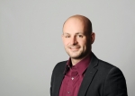

Erler, Martin

Erler, Martin

FlowLogiX GmbH

Erler, Martin

Abstract
Automated material handling systems (AMHS) are the future of intralogistics. Due to rising staff costs – especially in high-wage countries – the only way to stay competitive is to fully automate handling of materials inside the production. With increasing spread and size of such systems (e.g. AGV or OHT) the complexity on planning, monitoring and improving rises exponential. Main reason therefore is that each task is performed with a separate software although they actually share a lot of information. This leads to exploding affords on modelling, searching and data handling. As a result, some very useful tools like simulation studies become so expensive that they are rarely used.FlowLogiX Maintenance and Monitoring Suite (MMS) is a single browser-based application combining all tools needed to plan, monitor and optimize an AMHS. This enables completely new workflows. There is no more need to setup an internal simulation-project just figure out, whether the AMHS has enough capacity to handle the closed track due to maintenance next week. With just a few clicks inside the same application the result is available within seconds and presented in an understandable manner.Organizational and human boundaries between areas of work disappear and become small tasks in a single efficient workflow.

Biography
Martin Erler is passionate about sophisticated planning software and how it can support efficient workflows in companies. Martin started his career at Technische Universität Dresden in 2010 with researches on planning processes and techniques for cutting technology. He developed a method for fully automated estimation of roughing times based on CAD-Data. In 2015 he changed his field of research to intralogistics – especially automated material handling systems. He believes that those big systems are the future of intralogistics. As result of a software project for a big semiconductor manufacturer he decided to concentrate his experiences about good planning and put it into one software every company can buy. Today Martin is CEO and co-founder of FlowLogiX GmbH.

Young Disruptors
FocalSpec Ltd FocalSpec Ltd Deveci, Murat
Line Confocal Sensors for Industrial Inspection
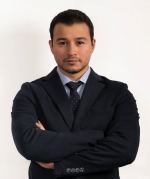
Deveci, Murat

Deveci, Murat
Sales Manager
FocalSpec Ltd

Deveci, Murat

Abstract
Line Confocal Imaging (LCI) is an optical technology for high speed 2D and 3D topography and tomography measurements.Line Confocal Imaging sensors measure millions of accurate data points per second, also from moving surfaces. The LCI sensors provide sub-micron resolution and can be used for all kind of surface types, including glossy, curved and transparent materials that have been challenging for industry standard laser sensors. Simultaneously with the 3D data, the LCI sensors produce also high dynamic range pixel synchronised intensity images of the surface which can be used to 2D defect detection and pattern recognition.The applications of LCI sensors include roughness measurement of transparent surfaces, defect detection in multilayer transparent materials, high speed dimensional control of 3D curved glasses, various surface and sub-surface analysis of flexible, hybrid, and organic electronics, BGAs, MEMS.The LCI sensors can be integrated to factory automation using Ethernet interface.In this talk, the LCI will be explained in detail and several industrial applications will be given as examples.Keywords: optical 3D sensors; surface metrology; film tomography, high-speed in-line inspection; submicron

Biography
Murat Deveci is responsible for market development and sales operations in Europe, the Middle East, and Africa as a sales manager. He has been working in sales and marketing of advanced metrology systems since 2012 within different companies. He holds a Master of Science degree in Materials Engineering from the Tampere University of Finland.

Exhibitor Presentations
Fraunhofe ipms Fraunhofe ipms Gerlich, Lukas
Interconnects, scaling and integrational aspects in 300mm R&D
Gerlich, Lukas

Gerlich, Lukas
Project manage
Fraunhofe ipms

Gerlich, Lukas

Abstract
New challenges in diversification of materials and in integration of new concepts in the Back-End-of-Line (BEOL) emerge with further development of novel computer chips. Besides scaling of feature sizes and usage of other substitute materials for Copper as interconnect or for barriers and liners like Cobalt new memory or capacitor stacks integrated in the metallization area give a lot of opportunities as a test platform for next generation computing and beyond CMOS approaches. But also some obstacles have to be resolved like material compatibility and contamination control. This is especially important for ferroelectric Hafnium Oxide based material and new materials for MRAM and general spintronic developments. Here we will present the memory integration concept in our BEOL with new Clover chambers in an AMAT Endura system with mixed protocol zone environment for flexible R&D on 300mm. Therefore within national-, EU-funded projects and direct contract research Fraunhofer IPMS works together with the industry for finding solutions to keep technology development for more-Moore and more-than-Moore applications on track.We will also address the additional requirements for consumable and tool manufacturers, which are connected with the progress of Moore’s law. Within the FMD (Forschungsfabrik Mikroelektronik Deutschland) new tool setups and with the help of our Screening Fab approach, we enable partners to optimize their products for future scaling and integration.

Biography
Dr. Lukas Gerlich (Fraunhofer IPMS) received his PhD (Dr.-Ing.) at Brandenburg Technical University Cottbus in 2012 in the field of barrier films for Cu-metallization on 300 mm wafers and in-situ XPS characterization during his work at Fraunhofer CNT together with AMD and Globalfoundries as project partners. Since the integration of Fraunhofer CNT into IPMS in 2013, he works as project manager and was responsible for BEOL thin films and plating module. Since 2019 he is staff scientist at the spintronic group and in charge for MRAM stack development, Screening-Fab activities and equipment control especially of the AMAT Endura platform. As scientist or project manager he was involved in several national (SAB/BMBF) and EU projects (Horizon2020/Ecsel) e.g. KuWANO, NoLimit, Evolve, Connect, WayToGoFast, Leistungszentrum-Waferhub, FMD.

Challenges of Moores Law
Fraunhofer-Institut für Integrierte Schaltungen IIS Fraunhofer-Institut für Integrierte Schaltungen IIS Loidl, Karin
5G for industrial Applications
Loidl, Karin

Loidl, Karin

Fraunhofer-Institut für Integrierte Schaltungen IIS

Loidl, Karin

Abstract
Still not available, it will follow

Biography
Karin Loidl has been with Fraunhofer IIS since 2004 and is an experienced, multidisciplinary engineer whose constant goal is to successfully bridge the gap between ideas, research, development, and implementation. Since Release 15, she has been actively involved in the standardization of 5G and, starting in 2017, has acted as the Fraunhofer IIS SA1 delegate within 3GPP.Karin’s focus within 5G lies on features enabling verticals to optimize the use of 5G for their specific applications. Her comprehensive knowledge of wireless communication solutions, current and upcoming, as well as radio-based positioning technologies, is founded on nearly 25 years of experience in creating and implementing such solutions and the necessary technologies. She graduated with a degree in telecommunication engineering from Ulm University and as an industrial engineer in international economic relation from Nuertingen-Geislingen University as well. From 1996, she worked for PHILIPS before joining Fraunhofer IIS. Apart from 3GPP SA1, she is also active in 5G ACIA, NGMN, VDMA and is a member of the Advisory Board of Global5G

Smart Manufacturing I (software-centric)
Fraunhofer EMFT Fraunhofer EMFT Leistner, Henry
Leistner, Henry

Leistner, Henry
Team Leader | Micro Dosing Systems
Fraunhofer EMFT

Leistner, Henry

Biography
Henry Leistner is holding a Master's degree in Semiconductor Physics and in Industrial Engineering. His previous research activities focused on yield enhancement methods at X-FAB Silicon Foundries. Further he investigated improvement strategies in customer supply allocation with machine learning at Infineon Technologies. Since 2018, he has been leading a team of the Micro Dosing Systems department of Fraunhofer EMFT, covering a broad range from applications, feasibility studies and consulting activities in medical technology (e.g. artificial pancreas, insulin patch pumps) to consumer electronics (e.g. environmental sensors in smartphones). Additionally, he is pursuing a PhD in Electrical Engineering at Technical University of Munich.

SMART MedTech
Fraunhofer EMFT Fraunhofer EMFT Richter, Martin
Precise Drug Delivery for Personalized Healthcare
Richter, Martin

Richter, Martin
Head of department
Fraunhofer EMFT

Richter, Martin

Abstract
Microdosing of drugs for personalised healthcare covers many different application. Subcutaneous delivery for the therapy of diapetes is the major target application, additionally new patch pump applications (for other high viscous drugs) currently rise up. To deliver the drugs for these patch pumps, piston pumps are state of the art, but limited to size and thickness of the patch pump system. Novel silicon micropumps with a chip size down to 3,5x3,5x0,6 mm3 have the potential to replace piston pumps and enable the vision of a ultra flat patch pump system. Additionally, cost efficent solutions for dosing monitoring, free flow protection, catheter blockage detection and bubble management have to be addressed.

Biography
Dr.-Ing. Martin Richter studied Technical Physics at the University of Munich and got his diploma 1992. He managed several microfluidic Projects in the 90ies, and finished his PhD work in the field of microfluidic systems 1998. Since 2000 he is managing the department DOS of Fraunhofer EMFT, he is responsible of a team of 14 scientists and 15 students. His main task is to establish new research cooperations with academic and industrial partners in the field of microdosing systems. Martin is author and co-author of more than 35 patents and around 80 publications in the field of microdosing systems.

SMART MedTech
Fraunhofer Group for Microelectronics Fraunhofer Group for Microelectronics Bressler, Patrick
Bressler, Patrick

Bressler, Patrick
Managing Director
Fraunhofer Group for Microelectronics

Bressler, Patrick

Biography
Patrick Bressler is currently the managing director for the Fraunhofer Group for Microelectronics. The group consists of 17 Fraunhofer Institutes with a total research budget of €439M and +3000 staff (2017), dedicated to technology development and technology-based innovation in micro- and nanoelectronics. Before that Dr. Bressler was the Executive Vice President of Fraunhofer USA, the US subsidiary with an annual budget of +$42M and +160 staff, and adjunct professor at the department of computer science and engineering at Michigan State University. Patrick has held various executive positions in Europe and the US, in basic research, technology validation and technology-based business and entrepreneurship, such as technology expert and Fraunhofer representative to the European Commission in Brussels. By training a physicist, Patrick holds a PhD in surface and semiconductor physics from the Technical University Berlin.

Disruptive Computing
Fraunhofer IISB Fraunhofer IISB Pfeffer, Markus
Pfeffer, Markus

Pfeffer, Markus
Group Manager
Fraunhofer IISB

Pfeffer, Markus

Biography
Dr. Markus Pfeffer (Fraunhofer IISB) holds a diploma in Electrical Engineering and a PhD (Dr.-Ing.) with specialization in manufacturing optimization both from the University of Erlangen- Nuremberg. Since 2002 he is with Fraunhofer IISB in the department Semiconductor Manufacturing Equipment and Methods. He is leading the group Manufacturing Control with a strong focus on equipment control, contamination control, manufacturing optimisation, equipment assessment and discrete event simulation. He was/is involved in several national and international cooperative R&D projects, e. g. FLYING WAFER, IMPROVE, EEMI450, EPPL, Productive4.0, idev40, NEREID, FED4SAE and SEA4KET in a variety of functions.

Challenges of Moores Law
Fraunhofer Institute Fraunhofer Institute Quay, Rüdiger
Diamond for Quantum Computing
Quay, Rüdiger

Quay, Rüdiger
Deputy Director
Fraunhofer Institute

Quay, Rüdiger

Abstract
Quantum computers exploit the phenomenon of quantum superposition, or the counterintuitive ability of small particles to inhabit contradictory physical states at the same time. An electron, for instance, can be said to be in more than one location simultaneously, or to have both of two opposed magnetic orientations. Where a bit in a conventional computer can represent zero or one, a qubit can represent zero, one, or both at the same time. It’s the ability of strings of qubits to simultaneously explore multiple solutions to a problem that promises computational speedups.Diamond-defect qubits result from the combination of “vacancies,” which are locations in the diamond’s crystal lattice where there should be a carbon atom but there isn’t one, and “dopants,” like nitrogen atoms placed in direct neighborhood to the vacancy. Together, the dopant and the vacancy create a donor-vacancy center, which has a free electron associated with it. The electrons magnetic orientation, or spin, which can be in superposition, constitutes the qubit. Donor-vacancy centers in diamond potentially can work at room temperature and are therefore considered a very attractive technology for building quantum networks. The biggest drawback to donor-vacancy centers in diamond is the difficulty of fabrication. Researchers either look for naturally-occurring defects in diamond, or fire atoms at a piece of diamond at high energy, creating defects in modulation doped lattice. We review the remarkable progress made in the past years in controlling electrons, atomic nuclei, and light at the single-quantum level in diamond. We also discuss prospects and challenges for the use of donor-vacancy centers in future quantum technologies.

Biography
Rüdiger Quay received the Diplom-degree in physics from Rheinisch-Westfälische Technische Hochschule (RWTH), Aachen, Germany, in 1997, and a second Diplom in economics in 2003. In 2001 he received his doctoral degree in technical sciences (with honours) from the Technische Universität Wien, Vienna, Austria. In 2009 he received the venia legendi (habilitation) in microelectronics, again from the Technische Universität Wien. In 2001 he joined the Fraunhofer Institute of Applied Solid-State Physics Freiburg in various positions. He is currently the deputy director of Fraunhofer IAF and responsible for the business fields. Since 2011 he is also a lecturer at the IMTEK, Albert-Ludwig University, Freiburg, Germany. Dr. Quay has authored and coauthored over 250 refereed publications, three monographs and contributions to two further. He holds two patents.

Disruptive Computing
Fraunhofer IPMS Fraunhofer IPMS Lakner, Hubert
Next Generation Computing
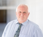
Lakner, Hubert

Lakner, Hubert
Director Fraunhofer-Institute for Photonic Microsystems IPMS
Fraunhofer IPMS

Lakner, Hubert

Abstract
The global digitization of all branches and value chains will henceforth only be possible with novel powerful computer systems. New generations of data centers and server farms are necessary for super-fast cloud computing. Additionally, next generation computers require decentralized, mobile, compact and highly efficient processor performance classes and will be used for edge computing and sensor nodes.As the conventional downsizing approach in processor development according to Moore’s Law is no longer sufficient, new concepts are required to allow ultra-fast processing, especially for artificial intelligence applications. Disruptive and highly innovative concepts that are based on artificial neural networks and neuromorphic processors for quantum computing will supersede the currently utilized “Von-Neumann-architecture”. The neuromorphic architecture is characterized by a large number of interconnections and parallel processors, tight collocation of processor and memory, high data transfer bandwidth and very low power consumption.The classic separation of hardware and software will be eliminated and therefore holistic system concepts could lead to novel solutions in the industrial sector. Coordinated developments in hardware-software-co-design enable solutions for future applications, e.g. autonomous driving. At the same time, existing and new systems need protection against cyber-attacks and have to be trustworthy. Thus, research into new architectures, design and manufacturing processes for computers and systems with a secure trust anchor, so called trusted electronics, is required.

Biography
Hubert Lakner (born 1958) received his diploma-degree in physics from Eberhard-Karls-Universität Tübingen in 1986. After one year in industry he joined the Gerhard-Mercator-Universität (Duisburg) working in the field of nanocharacterisation of mesoscopic semiconductor structures. He received his PhD in Electrical Engineering in 1993. From 1994 until September 1998 he hold a post doc position (Oberingenieur) at the Gerhard-Mercator-Universität. He focussed on high frequency and high speed circuits based on compound semiconductor heterostructures. In October 1998 he joined the Fraunhofer Institute for Microelectronic Circuits and Systems (IMS) in Dresden where he was the Acting Director in 2002. Since January 2003 he is the (founding) Director of the new Fraunhofer Institute of Photonic Microsystems (IPMS) in Dresden. Additionally, he is Professor for Optoelectronic Devices and Systems in the Department of Electrical Engineering and Information Technology at the Technical University Dresden since February 2004. He is chairman of the board of directors of the Fraunhofer Microelectronics Group since 2005, representing about 3500 employees in 11 Fraunhofer institutes, and member of the Fraunhofer Präsidium (Presedential Council).Prof. Lakner is engaged in many European and German initiatives e.g. AENEAS supervisory board, member of the ELG (Electronic Leaders Group), member of ECSEL Germany, chairman of the scientific advisory board of SILICON SAXONY.

Opening Ceremony & Keynote
Fraunhofer IZM Fraunhofer IZM Schischke, Karsten
A Circular Economy for Smartphones
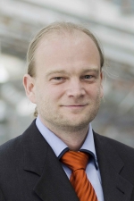
Schischke, Karsten

Schischke, Karsten

Fraunhofer IZM

Schischke, Karsten

Abstract
Some smartphone brands incorporate increasingly Circular Economy approaches in their business and design strategies. This presentation will adress some of these approaches and discuss the pros and cons of these. Design and product use patterns have to be a good match to yield a better "sustainability". Design concepts, such as various types of modularity, require e.g. a willingness of consumers to repair devices or manufacturers to put in place a return policy for used units. Modularity includes modules on the mainboard level, targeting at better reusability of individual functional blocks, but also fully open modularity platforms allowing third parties to build smartphone modules, which are compatible with those modules manufactured by others. Modularity however is not "for free": Modularity requires additional materials and components to connect and house modules. This has to be offset by a longer lifetime of the product. Circular design without changing economic cycles will not work out.At end of life research targets at better recyclability of some spice metals, which are not yet recovered in state-of-the-art smelters. Robotics are a way forward to extract components containing specific elements for a separate treatment. The presentation will give some insights in increasing the recycling potential through such approaches. Chosen examples are neodymium, tantalum and tungsten.Legislation and standardisation try to keep pace with these trends. Policy intends to regulate mobile ICT devices under the European ecodesign regulation. The presentation will touch on the latest developments and will give an outlook on possible consequences for the smartphone market.

Biography
Karsten Schischke is Group Manager Product Ecodesign and Circular Materials at Fraunhofer IZM and holds a degree in Environmental Engineering from Technische Universität Berlin. He has 19 years’ experience in applied research on sustainability of electronics. He has been involved in several technical product group studies in preparation of the EU’s eco-design product policy. Since 2008 he is coordinating large European research and innovation projects in the FP7 and Horizon 2020 programme, including projects on recycling of post-consumer plastics for new electrical and electronic equipment and eco-design of smart mobile devices. this latter project, sustainablySMART, involves large companies, such as AT&S, and small enterprises exploring circular concepts for mobile ICT devices, such as Fairphone B.V., Circular Devices Oy, MicroPro Computers, and Speech Processing Solutions. The presentation at SEMICON Europe mainly covers the findings from this H2020 project. Karsten supports the European Commission and stakeholders to implement the European EPREL database as part of the German National Top-Runner Initiative, financed by the Federal Ministry for Economic Affairs and Energy.

Building a Circular Economy in the Electronics Manufacturing Industry
Fujifilm Electronic Materials Fujifilm Electronic Materials Vanclooster, Stefan
Vanclooster, Stefan

Vanclooster, Stefan
Global Business Director Polyimides
Fujifilm Electronic Materials

Vanclooster, Stefan

Biography
Stefan Vanclooster is Global Business Director Polyimides at FujiFilm Electronic Materials (FFEM), located in Belgium. Stefan manages the global business unit of polyimide materials for the semiconductor industry within FFEM. Stefan received a Master’s degree in chemical engineering at the University of Ghent and a Master’s degree in Polymer and Composite Materials at the University of Leuven. He also obtained a postgraduate in business economics and finance at the University of Leuven

Strategic Materials Conference
Future Horizons Future Horizons Penn, Malcolm
Penn, Malcolm

Penn, Malcolm
Chairman & CEO
Future Horizons

Penn, Malcolm

Biography
Malcolm Penn is the Chairman, CEO and founder of Future Horizons, one of the world’s top global semiconductor industry analysts. He is also the President of Future Horizons' Moscow-based subsidiary, East-West Electronics, the world’s top market research consultant on the Russian and East European electronics industry.

Global Trade Disputes: a zero-sum game for all ― is there a way out?
Fyla laser Fyla laser Naujalis, Paulius
Two-photon absorption in semiconductors design and manufacturing
Naujalis, Paulius

Naujalis, Paulius
Sales Manager
Fyla laser

Naujalis, Paulius

Abstract
Two-Photon absorption technique for semiconductors and circuits inspection allows precise voxel analysis in semiconductors, wafers or circuits. High flexibility new fiber laser design allows to reduce costs from existing techniques and increases flexibility in measurement capabilities.

Biography
Experienced Sales Manager/Applications Specialist with a demonstrated history of working in the photonics industry. Skilled in Relationship management, commercial department management, design and development of photonics solutions and Research and Development (R&D). Strong engineering and commercial professional with a Master in Physics, Diploma in Engineering and Certificates in Business Management.

Exhibitor Presentations
G To top
GE Research GE Research Potyrailo, Radislav
Bridging the Gap from Semiconductors to Medical Technologies: GE Research Advances in Multiparameter Gas, Physiological, and Biological Sensing
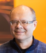

Potyrailo, Radislav

Potyrailo, Radislav
Principal Scientist
GE Research

Potyrailo, Radislav

Abstract
Modern monitoring scenarios for biomedical, biopharmaceutical, and personal wellness applications demand sensors with higher accuracy, enhanced stability, and lower power; all in unobtrusive form factors and at a low cost. Unfortunately, available sensors based on traditional detection principles are often inadequate in accuracy, stability, power demands, and convenience. It does seem that existing sensing concepts are reaching their fundamental performance ceilings. These limitations of available sensors drive the innovative designs of new generation of sensors. In our talk, we will discuss how technological advances in diverse segments of the semiconductor industry positively impact designs and performance of innovative types of gas, physiological, and biological sensors. We will present examples from our recent programs at GE Research where we focus on new principles of sensing based on multiparameter signal excitation and detection. We will demonstrate how these advances were achieved and implemented by utilizing diverse semiconductor processes. These developments resulted in sensors with previously unthinkable performance characteristics in wearable, stationary, and other form factors. As examples, we will illustrate the capabilities of these sensors to independently quantify different environmental, physiological, biological, or bioprocess parameters, to reject interferences, and to enhance sensor-response stability. Conventional and innovative semiconducting processes have played a major role in achieving our new performance characteristics.

Biography
Dr. Radislav Potyrailo is a Principal Scientist at GE Research, leading the growth of wireless and wearable chem/bio sensors for diverse applications. Radislav has been Principal Investigator on programs funded by GE, AFRL, DARPA, DHS, NETL, NIH, NIOSH, and TSWG. Some of these results Radislav summarized in 125+ granted US Patents and 150+ publications on transducer technologies, sensing materials, and data analytics describing sensing concepts and their implementations. He has delivered 80+ invited lectures and ten keynote/plenary lectures at national and international conferences and coauthored/coedited eight books. Examples of his contributions to scientific community include serving as the Chair of the MEMS and Sensors Industry Group (MSIG) Device Working Group, as the North America Regional Chair of International Society for Olfaction and Chemical Sensing, the initiator and a co-organizer of the First Gordon Research Conference on Combinatorial and High Throughput Materials Science, and as the editor of the Springer-Nature book series Integrated Analytical Systems. His recent recognitions include SPIE Fellow and Prism Award by Photonics Media/SPIE.

SMART MedTech
GE Research GE Research Cho, Sanghee
Cho, Sanghee

Cho, Sanghee
Lead Scientist Controls and Optimization
GE Research

Cho, Sanghee

Biography
Dr. Sanghee Cho is a Lead Scientist in Controls and Optimization group at GE Research. She Joined GE in 2014 after obtaining her Ph.D. in Statistics from Yale. At GE, Dr. Cho used her deep knowledge in Statistics to tackle a wide range of industrial challenges ranging from oncology, industrial asset performance & reliability, and quantification of financial risk. For the past two year, Dr. Cho has been a key member of multiple government-funded program where she leveraged her expertise in data analytics to analyze single cell data from multiplexing images on different cancer types.GE Research is a multi-disciplinary R&D center leading the digital transformation of industrial fields and providing innovative biomedical solutions for diverse healthcare applications, including bioelectric medicine, medical imaging, predictive medicine, monitoring and molecular diagnostics. The recent evolution of AI-based modeling and image analytics has enabled the development and implementation of new approaches in medical image analysis. The data extraction of biomarkers and features, in concert with genomics and proteomics, has unlocked a new era in therapy, diagnosis and prognosis. The use of AI/ML, enabled by big data analytics, will lead to the discovery of disease mechanisms, and contribute to better prognosis models, improving the prediction of therapy response and diagnostics. GE Research is taking a thought leadership position by supporting the fundamental research of how AI/ML will guide personalized medicine, cancer treatment, and the role of cyber security in delivering medicine in trusted transactions.

SMART MedTech
Global ZEUS Global ZEUS Chung, Mark
ZEUS (Cleaning Equipment)
Chung, Mark

Chung, Mark
President, N. America
Global ZEUS

Chung, Mark

Abstract
Global Zeus: A leader in semiconductor process equipment (wet bench and single wafer) as well as robots and advanced technology.Zeus has grown alongside the development of the Semiconductor, LCD, LED, renewable energy and IT industries. Regardless of the customer’s geographic location or their specific needs and requirements, our company provides the highest quality in available solutions and excellence in customer relations support. This has been our unwavering goal and entrepreneurial spirit for over the last 40 years and it will continue to drive our motivation and enthusiasm towards good business practices. Through this objective, we have maintained our role as a total solution provider, implicitly partnering up with other sources to deliver a variety of products and solutions for the Semiconductor & LCD industries. These products and services include cleaning equipment, HP/CP, In-Line software (CIM), chemicals, parts, and robots. As an enterprise with more than 40 years of direct industry experience, we are thoroughly preparing for a second leap into becoming a global leading company by developing new fields of business. In order to achieve this accomplishment, we will improve the value of our customer relations by applying more distinctive and competitive ideas into the equipment that we make. On top of fundamentally applying pioneering measures to our equipment, as a team all of our employees will desperately strive to further advance the company abroad under the flag of global Zeus.

Biography
Mark Chung is the president of the N. America organization for Global Zeus. He is leading the global growth initiatives for Global Zeus, helping customers find solutions for their challenges for improved performance and better cost of ownership. He has been in the semiconductor industry for most of his career, beginning as a process engineer at IBM, and progressing in his career to sales, management, investor relations, and executive positions. Prior to joining Global Zeus, he was president of Brooks Korea for 8 years, successfully leading market share gains, operational excellence, and customer satisfaction. He has a B.S. in Chemical Engineering from Northwestern University and MBA from Duke University.

Connect Korean Suppliers with European Customers
Globalfoundries Globalfoundries Capecchi, Simone
Chip Package Interaction Test structure design to address challenges from products with RF specific back end of line metallization options on Flip Chip ETS substrate
Capecchi, Simone

Capecchi, Simone
MTS Reliability Engineer
Globalfoundries

Capecchi, Simone

Abstract
The growing interest in applications for 5G communication has generated some efforts in developing new Back End of Line (BeoL) schemes in the Semiconductors industry. In particular, BeoL stacks with Ultra Thick Metal (UTM) for RF mmWAVE applications have come to the forefront. However the high thickness of the UTM (~3um) can induce significant residual stress, which brings up new challenges related to wafer and die warpage. The die warpage becomes quite critical during the temperature cycle that the silicon die undergoes during the flip chip assembly process.In addition, the market pressure to reduce assembly costs in packaging is driving the use of coreless Embedded Trace Substrates (ETS). The use of low cost substrates such as ETS can potentially reduce the assembly process margins: an ETS coreless substrate can be more prone to warpage during the assembly process than core substrates. The combination of silicon die and ETS substrate warpage can cause assembly yield loss as well as potential reliability issues.In this work we present the study of a Chip Package Interaction (CPI) test vehicle, with a Cu double Ultra Thick Metal implemented in a GLOBALFOUBDRIES 22FDX® BeoL stack. This test vehicle has been assembled using an Embedded Trace Substrate (ETS). This work is focusing on testing CPI structures that have been implemented to catch warpage and stress related fails through electrical test before and after the reliability environmental stress. Three different types of CPI sensor structures have been designed and implemented in the CPI test vehicle, in order to detect cracks in the BeoL and die warpage driven fails during and post assembly.Assembled dies of this test vehicle have undergone JEDEC standard reliability environmental test stresses. In conclusion, the GLOBALFOUNDRIES 22FDX® double UTM BeoL used in this work proved to be robust enough to pass the JEDEC standard reliability environmental test stress in a standard flip chip package with ETS substrate.

Biography
Simone CapecchiMember of Technical Staff, Reliability EngineeringGlobalfoundries, Dresden, GermanySimone Capecchi is currently employed as Member of Technical Staff in the Reliability Engineering Group of Globalfoundries in Dresden, Germany. The focus of his work is on Chip Package Interaction Reliability.Still in Globalfoundries Dresden, Simone spent four years in the wafer bumping engineering group sustaining high volume production as well as introducing new technologiesPrior to joining Globalfoundries, Simone lead an engineering group in STMicroelectronics for 3 years.Simone also worked as Senior Engineer in Intel Ireland and Intel US, sustaining high volume production as well transferring technologies from the development site to a high volume manufacturing site.Simone has also experience in the optical components fabrication in Nortel Networks where he developed processes for telecommunication components.

Advanced Packaging Conference
Globalfoundries Globalfoundries Madani, Ramin
Digital Twin / Ion Source Prediction
Madani, Ramin

Madani, Ramin
Sr Staff Project Manager
Globalfoundries

Madani, Ramin

Abstract
The ion source is a major concern in utilising implant tools to their full potential. The issue is mostly related to the thermionic filament which either exhibits beam imaging problems or sudden fusing. This work is examining both failure modes by implementing different prediction models. It can be demonstrated that the combination of different prediction models can enhance the overall accuracy of the prediction. The best prediction accuracy is achieved by combining linear regression methods with random survival forest as well as exponentially gradient-boosted trees.Moreover a fusing event can be predicted within 24 hours before occurrence in more than 75% of breakdowns and uniformity issues are forecast with a minimum accuracy of greater than 50% of the cases.The achieved accuracy has enabled the introduction of the predictive maintenance strategy for implant tools at Globalfoundries which has led to an improved utilisation and a reduction of 12.7% of total maintenance costs. Taking into account additional influences such as cycle time, mean time to failure or time to repair it can be shown that with a balanced approach additional 4.7% of cost saving is achieved.Based on this outcome the general condition for successfully applying predictive maintenance is discussed. In particular the process of identifying potential opportunities is highlighted. Dependencies in scaling this method effectively are studied with regards to: a) available feature information, b) the opportunity to generate run to fail data and c) easy access to failing components.

Biography
Dr. Ramin Madani studied Physics and worked at the Max-Planck-Institute for Plasma Physics in Greifswald until 2004 before joining Infineon/Qimonda at the 300 mm site in Dresden. He joined Odersun AG, a German manufacturer of flexible CIS solar film, in 2009 and was responsible for backend manufacturing. In 2012 he started at Globalfoundries where he initially led projects in the area of process control and successfully reduced tool variability to pave the way for a steady increase in 28nm LPQ prime yield - a major success for Fab1. He later headed a multi-year program to drive manufacturing excellence with sophisticated tool data processing and best in class automation solutions. In line with Globalfoundries’ smart manufacturing initiative, he launched in 2016 the equipment and process analytics program which is currently driving data intelligence and ML use cases in Fab1 manufacturing.

Fab Management Forum
H To top
Harbor Electronics Harbor Electronics Bleakley, Tom
Stretching the Performance Envelope of ATE PCBs
Bleakley, Tom

Bleakley, Tom
VP Integration
Harbor Electronics

Bleakley, Tom

Abstract
In today's production test environment, high power, high speed, high ball count, tight pitch and increased parallelism drive complexity into the ATE interface / probe card PCB. These factors inevitably drive PCB layer counts up, beyond what can be achieved in single lamination printed circuit boards, forcing more expensive and time consuming processes such as sequential lamination and HDI techniques.This presentation will discuss PCB fabrication constraints, technology extenders and introduces an alternative to standard PCB processing techniques. Power integrity, signal integrity, manufacturing throughput and reliability characteristics of available options will be compared. Specific examples to be discussed include: -Multitier PCB with 0.3mm DUT pitch in a 310mil thick PCB. -Memory test application with 100,000 pads and via interconnects in a 600mil thick PCB -WLCSP application with 0.35mm pitch in a 250 thick PCB

Biography
Tom Bleakley is Vice President of Integration at Harbor Electronics where he oversees PCB design, assembly and test, applications and field service engineering. Tom’s team is responsible for ensuring that Harbor PCBA designs integrate well with fab, assembly and field support operations, optimizing probe card and load board PCBA performance as well as delivery times. Tom has spent his entire career in semiconductor test. Before Harbor with Everett Charles Technologies as a Product Manager. Before ECT, Tom served in Product Engineering and Test Technology roles with Intel’s Desktop Chipset group in Folsom, CA, and with Intel Communications group in Sacramento, CA. Tom began his career as a hardware design engineer with Micro Component Technology (MCT) in Shoreview, MN designing DC parametric and pin electronics hardware before moving to an Applications Engineering role. Tom holds a bachelor of science degree in electrical engineering (BSEE) from North Dakota State University.

Advanced Packaging Conference
Henkel Corporation Henkel Corporation Trichur, Ramachandran
Advanced Assembly Materials for Enabling Heterogeneous Integration and System-in-Package (SiP) Applications
Trichur, Ramachandran

Trichur, Ramachandran
Director, Global Head of Advanced Packaging Market Segment
Henkel Corporation

Trichur, Ramachandran

Abstract
For a majority of the wafer fabs and applications, as the front-end lithography nodes move towards 7nm and lower, the upfront cost of the photolithography equipment and the total cost of ownership of the process outweighs the benefit gained from this technology. Only less than a handful of manufacturers can continue to invest in the bleeding edge front end lithography technology. Due to technological complexity of such processes, the pace of node shrinkage has slowed down sharply compared to Moore’s law. In the last few years, backend packaging technology has moved from being considered an afterthought for assembling the silicon device to the forefront for improving the performance of the packaged device. Mega trends like big data, artificial intelligence, 5G connectivity and autonomous driving applications are the drivers for advanced packaging of semiconductor devices. Advanced packaging enables these next generation devices to have higher bandwidth, faster processing speeds, reduction in form factor, reduction in total cost of packaging, and other benefits depending on the packaging technology used. Advanced packaging architectures present a myriad of assembly challenges that require innovation in packaging materials and processes. Requirements for packaging density, performance and cost vary between end applications such as mobile, high performance computing and automotive components. Various challenges are addressed by advanced packaging materials in all these applications.In this paper, we will present the pain points of advanced packaging methods and recent advancements in assembly material technologies for encapsulation using liquid compression molding (LCM), underfills (CUF, NCP NCF), warpage control, electro-magnetic interference (EMI) shielding materials that enable these advanced packages. Advanced assembly material development is critical to meet the stringent performance and packaging requirements for high performance micro-electronic devices.

Biography
Ram Trichur is the Global Head for Advanced Semiconductor Packaging Market Segment in Henkel’s Adhesives Technology division. Ram has 19 years of experience in the microelectronics industry covering both the front-end wafer processing and backend assembly processes, 3 patents with over 40 publications and technical articles in leading industry conferences and magazines. Ram received his master’s degree in Electrical Engineering from University of Cincinnati and completed his executive education in business management from Stanford University’s Graduate School of Business.

Advanced Packaging Conference
Henkel Electronic Materials Henkel Electronic Materials de Wit, Ruud
Innovative Interconnect and Encapsulation Developments for Wafer Level Packaging
de Wit, Ruud

de Wit, Ruud
EIMEA SU Head Semiconductors
Henkel Electronic Materials

de Wit, Ruud

Abstract
Smart Electronics’ trends like Big Data, Artificial Intelligence, Autonomous Driving and 5G continue to drive advanced semiconductor innovation towards higher functionality with smaller form factors and reduced power consumption. To meet these future demands, semiconductor package designs continue to evolve towards WAFER scale assembly using 3D Stacking and System-in-Package (SiP) type of architectures. Through Silicon Via (TSV) is enabling 3D die stacking for High Bandwidth Memory (HBM) allowing for finer pitch. Wafer Level Packaging (WLP) for both Fan-In and Fan-Out are also gaining momentum rapidly and same for Panel Level Packaging (PLP) showing significant progress. With this move towards SiP, increasing data demands, faster processing speeds and the emergence of 5G, traditional wafer fabrication companies are getting more in the driver's seat of Semiconductor Packaging.New finer pitch interconnect and low warpage encapsulation developments are essential for such high-density and challenging 2.5/3D device manufacturing processes, stress management for larger devices and increasing long-term reliability requirements. Next to this, increasing heat generation and dissipation, Fan-In and Fan-Out process compatibility (adhesion, die shift) and further need for miniaturization (Keep-out-Zone) are key challenges for Semiconductor Packaging material suppliers. < div >This presentation will give a technical overview of the advanced wafer level packaging material developments to enable next gen 2.5D and 3D chip designs :< div >- “Wafer Applied Underfill Films” for 3D Stacking of thin TSV wafers with increasing thermal performance and faster processing- Low shrinkage and ultra-low warpage wafer encapsulants and coatings for Fan-In and Fan-Out applicationsThese developments are aimed to meet the market's sustainability, miniaturization and high reliability requirements with providing reliable, scalable and environmental-friendly adhesive and encapsulation solutions.

Biography
Ruud de Wit is responsible for managing Henkel's Semiconductor Packaging Materials business development within EIMEA region. Ruud has a BSc degree in Mechanical Engineering followed by several polymer, sales and marketing courses. Ruud is working for Henkel since 1990 in multiple positions including technical customer service, quality assurance and engineering, and global semiconductor account and product management.

Strategic Materials Conference
Hewlett Packard Enterprise Hewlett Packard Enterprise Esteban, Susana
Advancing the Way People Live and Work

Esteban, Susana

Esteban, Susana
Worldwide Quality Customer Research
Hewlett Packard Enterprise

Esteban, Susana

Abstract
Hewlett Packard Enterprise (HPE) is a global technology leader focused on developing intelligent solutions that allow customers to capture, analyze, and act upon data seamlessly from edge to cloud. HPE enables customers to accelerate business outcomes by driving new business models, creating new customer and employee experiences, and increasing operational efficiency today and into the future.During the SMART Workforce Forum, as part of the SEMICON Europe 2019 (Munich, Nov 12th), HPE will share with the audience about the Company’s purpose, and values including its full commitment to Inclusion & Diversity which is key to Hewlett Packard Enterprise’s foundation principles.At Hewlett Packard Enterprise, we believe that the full power of our people will drive HPE success. A focus on Inclusion & Diversity helps to drive new business, fuel innovation, and attract and attain the best employees. It makes a difference in the workplace, marketplace, and community advancing the way we live and work. We make it matter.

Biography
Joined HPE in 2002 to take leadership role in Services Quality and Customer Experience.Prior to HPE, held key leadership positions in AT&T Microelectronics and Lucent Technologies.29 years experience in services and manufacturing industries and disciplines such, production control, customer service, public affairs, quality management and customer research.Master degree in Physics (Complutense University of Madrid) and Master degree in Strategic Quality Management (Portsmouth Business School).Certified Six Sigma Black Belt and Lean Expert.Based in Madrid, Spain. Married, two children, both students attending college and high school.

SMART Workforce
HQ-Dielectrics GmbH HQ-Dielectrics GmbH Niess, Juergen
Thermal Treatments in MEMS Fabrication:Challenges and Benefits of Rapid Thermal Processing (RTP)
Niess, Juergen

Niess, Juergen
Director Technology
HQ-Dielectrics GmbH

Niess, Juergen

Abstract
Thermal treatment in general, but also Rapid Thermal Processing (RTP) in particular, are well established processing technologies in semiconductor manufacturing [1] , [2]. Even though MEMS fabrication is using the same fundamental technologies and methods, there are new challenges coming up with new device layouts and structures.Whereas most advanced processing technology in semiconductor device fabrication is done and available for 300 mm wafers, the highest performance requirements in MEMS fabrication are needed for 150 mm and 200 mm wafer size. As a consequence, there is a lack of equipment, addressing the technology needs of MEMS device manufacturing on relevant wafer size.Furthermore thermal mass distribution on semiconductor device wafers is rather uniform along the wafer radius, whereas MEMS devices often exhibit areal distributions of etched trenches and holes, having a distinct influence on thermal mass and its distribution over the wafer. Especially during the non-equilibrium phase of a thermal treatment, these areal variations have a strong influence on heating rates, soak times, and maximum temperature over the wafer.Last but not least, specific materials combinations, e.g. for contact formation, with specific properties (durability in harsh media, at elevated temperature,…) are requested in MEMS device technology, which have to be characterized and understood in terms of reaction kinetics e.g. with silicon, in terms of deposition behavior, and last but no least in terms of thermal treatment.The present publication discusses the various influences and challenges, and introduces potential technologies addressing those challenges. Using the example of pressure sensors, the efficiency of used methods is discussed.

Biography
Dr. Juergen Niess holds a diploma on physics and a PhD with specialization in solid state physics, both from the University of Ulm, Germany. He has 20+ years of experience in rapid thermal processing (RTP) technology and equipment development with respect to Si processing as well as compound semiconductor processing. He also has several years of experience in plasma oxidation resp. nitridation and related equipment specification and development. His experience is documented through multiple papers that were authored and co-authored by him as well as a book on “rapid thermal processing and beyond”, which was edited by him. He also holds patents in the field of RTP and plasma oxidation and has several patents pending.

MEMS along the Value Chain
I To top
Ibm Ibm Corti, Elisabetta
Advances in Energy Efficient Neuromorphic Computing: Ready for Artificial Intelligence at the Edge?
Corti, Elisabetta

Corti, Elisabetta
researcher in the Science & Technology
Ibm

Corti, Elisabetta

Abstract
In this presentation we will present most recent technological advances in neuromorphic computing and their readiness to serve energy efficient artificial intelligence applications from Cloud to the Edge, with emphasis on Edge AI applications and challenges. We will particularly present progress in memristive and phase-change technologies for neuromorphic devices and system archhitectures, in comparison with CMOS implementations. We will address questions such as : (1) will spike-based neuromorphic systems be more successful than the artificial neural networks and (2) can they really be much faster and more efficient than biology? We will outline trends and challenges in the path towards successful implementations of learning systems that could be ubiquitously deployed for a large variety of cognitive computing and sensing at the Edge.

Biography
Elisabetta Corti is a researcher in the Science & Technology department at IBM Research, Zurich. In parallel, she is working towards a Ph.D. degree in Electrical Engineering under the supervision of Prof. Adrian Mihai Ionescu at EPFL, Lausanne. Her research focuses on advanced and exploratory architectures for neuromorphic computing applications. In 2018 she presented her work at the International Conference of Rebooting Computing, held in the framework of The International Roadmap for Devices and System, a research and industrial summit to project the future 15-20 years of electronic technologies. Prior to her engagement with IBM and EPFL, Elisabetta interned at imec, Belgium, researching structures for spinwave-based devices for logic applications. She holds a Master degree in Electronics Engineering from Politecnico di Milano, Italy.

Disruptive Computing
IBM Research IBM Research Curioni, Alessandro
Future of Computing: bits + neurons + qubits
Curioni, Alessandro

Curioni, Alessandro
Academy of Technology LogoIBM Fellow, Vice President Europe and Director IBM Research - Zurich
IBM Research

Curioni, Alessandro

Abstract
One of the promising applications for quantum computing is in Materials and Chemistry. With a quantum computer scientists and engineers expect to untangle the complexity of molecular and chemical interactions leading to the discovery of new materials and medicines, and model the quantum states of molecules.Other potential application areas are Business Optimization, supply chains, logistics, modeling financial data, and risk analysis

Biography
Dr. Alessandro Curioni is an IBM Fellow, Vice President of IBM Europe and Director of the IBM Research Lab in Zurich, Switzerland. On top of being responsible for IBM corporate research in Europe, he coordinates global research in IoT and Security. Dr. Curioni is an internationally recognized leader in the area of high-performance computing and computational science, where his innovative thinking and seminal contributions have helped solve some of the most complex scientific and technological problems in healthcare, aerospace, consumer goods and electronics. He was a member of the winning team recognized with the prestigious Gordon Bell Prize in 2013 and 2015. His reserch interests now include AI, Big Data and novel compute paradigms, such as neuromorphic and quantum computing.Dr. Curioni received his undergraduate degree in Theoretical Chemistry and his PhD from Scuola Normale Superiore, Pisa, Italy. He started at IBM Research – Zurich as a PhD student in 1993 before officially joining as a research staff member in 1998, where he had several research and manager roles, including being the founding manager of the Cognitive Computing and Computational Sciences department. He is a member of the Swiss Academy of Technical Sciences .

Opening Ceremony & Keynote
Ibm Services Ibm Services Kobusch, Ingo
Democratizing AI to accelerate the journey towards smart manufacturing
Kobusch, Ingo

Kobusch, Ingo
Industry Consultant, IBM Global Electronics Center of Competence
Ibm Services

Kobusch, Ingo

Abstract
Semiconductor manufacturing has been at the forefront of implementing aspects of smart manufacturing since the early 2000s. Automated material handling and analytics have enabled 300mm fab to reach the highest level of automation among almost all manufacturing industries. Artificial Intelligence (A.I.) holds the promise of driving the next level of smart manufacturing. This talk will cover how to accelerate the application of AI and advanced analytics in semiconductor manufacturing by combining semiconductor domain specific templates and solution patterns utilizing advanced AI & Machine Learning algorithms via hybrid multi cloud delivery model.

Biography
Ingo Kobusch is member of IBM’s Global Electronics Center of Competence. He has over 20 years of experience in semiconductor manufacturing and electronics manufacturing and operations. He combines deep industry knowledge with first-hand experience in designing and implementing manufacturing control and optimization systems and processes. Recently, his work has focused on digital transformation, advanced analytics & AI, Industry 4.0 and cognitive manufacturing.

Smart Manufacturing I (software-centric)
IC'Alps IC'Alps Girin, Remy
Enabling Smart MD with Custom Integrated Circuit (ASIC)
Girin, Remy

Girin, Remy
Business Development Manager
IC'Alps

Girin, Remy

Abstract
In the context of the digitalization of Medical Devices (MD) and of the associated revolution of the Internet of Medical Things (IoMT), there is a growing need for optimized electronic.Today, the most widely used approach to develop MD products is electronic boards implemented using Components Off-The-Shelf (COTS) or FPGA, with performances, content and form factor as they are. No customization and limited optimization is possible which does not really match the stringent medical application requirements.We can now demonstrate that ASIC approach shows decisive advantages for medical applications and especially for implanted medical devices.People may think that custom integrated circuit (ASIC) is a way too expensive for their device. But, thanks to the constant decreasing cost of silicon, the possibility for medium to low volume applications to benefit from an ASIC becomes a reality.An ASIC is a circuit designed to do exactly what you need and nothing more, with the required level of quality (ISO13485 compliant for medical). Consequently, it facilitates miniaturization through small chip footprint and drastic BoM reduction, it enables extreme low power consumption, a key parameter to optimize the autonomy.Furthermore, as you own the ASIC, you will have full control of your chip procurement with a low sensitivity to obsolescence, that is useful when product life ranges more than a decade.Always with the willingness to make easier the life of MD developers, IC’Alps is working on a new Medical Optimized multi-sensor Platform (MOPx). It offers an industrial solution containing various physiological readouts (ECG, PPG, GSR, Bio-Z), power management features to optimize battery life time, security functions to guarantee data integrity, processor for algorithms and wireless communication for remote data collection and control. This MOPx platform will help MD developers to accelerate and secure the way from the POC to the industrialized MD product.

Biography
Graduated in Electrical Engineering in 2004, Remy GIRIN developed his technical, management and business knowledge in the semiconductor market for nearly 15 years. He participated numerous European collaborative projects for bringing disruptive innovations to the market. After having encountered success in helping growing the innovation and turnaround the operations in his previous company, Remy joined IC’Alps just after registration in 2018 a company specialized in ASIC design in particular for medical applications, and is now committed to raise IC’Alps’ business.

SMART MedTech
IHP IHP Mai, Andreas
High performance photonic technologies for communication and sensing applications
Mai, Andreas

Mai, Andreas
Department Head
IHP

Mai, Andreas

Abstract
Photonic integrated circuits (PICs) have been subject of intense research and gained increased attention during last decades. Different wafer level technologies based on silicon-on-insulator offer platforms for novel advanced application areas as high data rate communication and photonicbio-sensing. Silicon photonic devices have the advantage that they are highly capable of being integrated, which allows an efficient combination of electronic and photonic devices with digital and analogue devices in electronic-photonic-integrated circuit (EPIC) technologies. However, silicon has drawbacks in terms of material properties and therefore in performance. In this talk, we present current progress in joint module developments of SiGe heterojunction bipolar transistors and related BiCMOS technologies in conjunction with monolithic integrated silicon photonic components. Moreover, recent results of novel integration concepts will be presented showing the potential to overcome material limitation of silicon in terms of electro-optic effects. This is followed by a brief overview of silicon-based photonic sensors for biochemical sensing. We discuss integration concepts, which are compatible to standard CMOS technologies showing the potential for future high performance silicon photonic technologies.

Biography
Prof. Dr. rer. nat. Andreas Mai received his diploma degree in physics from the Technical University of Brandenburg jointly with AMD Saxony in 2006 and his PhD in 2010. He joined the “Process Integration” group of IHP Technology Department in 2006 and he focused on the development of a 130nm SiGe-BiCMOS technology for mm-wave applications and the integration of RF-LDMOS transistors. He became group leader of the “Process Integration” team at IHP in 2012 and Head of the “Technology-Department” in 2015. Since 2018 he hold a professorship at the technical University of Applied Science Wildau for “Micro- and Nanoelectronics”. He is an IEEE member, Chair of the “ECS-SiGe Processing” symposia and head of the Joint-Lab between University of Applied Sciences Wildau and IHP.

Smart Photonics
IHS Markit IHS Markit Akhtar, Noman
Factors Affecting the Market Landscape for Sensors
Akhtar, Noman

Akhtar, Noman
Analyst - Industrial Semiconductors and Sensors
IHS Markit

Akhtar, Noman

Abstract
Sensors are found in a wide range of applications and industry sectors and the market is as a result in good health overall. While consumer sensors are adopted rapidly and wax and wane rather more quickly as markets, new sensing applications quickly emerge to keep MEMS sensor suppliers busy. While smartphones still represent a huge market, commoditization has left it saturated in value terms, but growth has recently moved to other accessories like smart watches or wireless earbuds from leading suppliers like Apple. Such devices are becoming very smart, involving multiple accelerometers and silicon microphones per set, and potential further functionality on the way in the form of heart rate, even oxygen saturation, and blood pressure. Talking of pressure, this sensor was recently adopted in e-cigarettes for puff detection. Other mainstays like automotive and industry, on the other hand, are subject to longer-term trends like electrification and robotization of the car, as well as Industry 4.0, big data and condition monitoring. Meanwhile, autonomous cars or taxis are not the only markets to watch: automation of many functions is taking place, e.g. in smart cities, smart building such as warehouses and logistics operations, in logistics and package tracking, in drones for surveying and mapping. Agriculture is also benefiting from sensors, drones are used for crop spraying, for example, and other sensors are used to monitor other key metrics like acidity, etc. Robotics and automation implies many sensing devices including position, motion and pressure sensors. This presentation looks at the impact of these major market changes on MEMS and other silicon sensors.

Biography
Mr. Noman Akhtar, a research analyst at IHS Markit, focuses on the Industrial market dynamics on semiconductors and sensor. Noman shares his expertise with the IHS Markit semiconductor team and leverages his deep understanding of the impact on industrial sensors and semiconductors along with analyzing its supply chain.He has deep technical knowledge in electronic component especially power electronics component in industrial semiconductor applications such as in factory automation, lighting, security, energy, medical, power and energy, military and aerospace segments systems. He manages the data quality of IHS Markit semiconductor and sensors market share databases and its timely delivery to clients. His responsibilities also include the synthesis of worldwide economic trends to help generate accurate market forecasts. Prior to this, Noman Akhtar led IHS Markit smart city intelligence service and had developed a broad understanding of smart cities project, related technologies, and regional business strategies. He also has a strong understanding of smart home appliances, robots and their semiconductor BOM within the consumer electronics segment. Noman joined IHS Markit in May 2014. Noman holds a Master of Science in Power Engineering specializing in power electronics in smart industry, smart home and smart grid electronics from the Technical University of Munich, Germany and a Bachelor of Science in Electronic Engineering from Sir Syed University of Engineering and Technology in Karachi, Pakistan. He is based in Munich, Germany.

MEMS along the Value Chain
IMAPS Germany IMAPS Germany Mueller, Jens
Mueller, Jens

Mueller, Jens

IMAPS Germany

Mueller, Jens

Biography
Jens Müller received his diploma degree for electrical engineering and the doctoral degree from Ilmenau University of Technology, Ilmenau, Germany, in 1992 and 1997 respectively. From 1997 to 2005, he held managing positions in development departments at Micro Systems Engineering GmbH, Berg, Germany. His responsibilities included research and development of medical implants (especially heart pace makers) and general substrate and packaging development (e.g. LTCC, flex-circuits, Chip Scale Packaging).In 2005, he returned to Ilmenau University of Technology to establish the junior research group “Functionalised Peripherics”. In July 2008 he was assigned full professor for the department of Electronics Technology at the same university. His research interest covers functional integration for ceramic based System-in-Packages considering aspects of harsh environmental use, and high thermal / high-frequency requirements with a strong focus on LTCC materials.From 2012 to 2018 he was the director of the Institute for Micro- and Nanotechnologies MacroNano® at his university.He joined IMAPS Germany in 1992 and worked in the board as vice president and president between 2000 and 2010. He also organized/co-organized various national and international IMAPS conferences and supported as technical program member the SEMI Advanced Packaging Conference for more than 13 years.

Advanced Packaging Conference
imec imec Leray, Philippe
EUV lithography insertion for future nodes in imec
Leray, Philippe

Leray, Philippe

Imec

Leray, Philippe

Abstract
The development of EUV lithography was a long journey, but its adoption as a solution for the industry in the coming node is now clear. But still some challenges are in front of us: Resist and Infrastructure.In this paper, after an overview of the landscape of the patterning development sustaining the Moore’s law, we will show the most recent results obtained in imec with our NXE3400. After the description of the hypothesis of physical/chemical mechanisms that seem to drive the stochastic problem, we will list all the initiative currently ongoing in imec to reduce the number of stochastic counts (resist, source, track process). We will describe our Attosecond laboratory initiative to investigate the fundamentals of stochastic defects creation. We will show the latest results about EUV mask impact on defectivity and the development of CarboNanoTubes pellicle (CNT). Finally, we will summarize by discussing the remaining challenges and what could be the role of High NA lithography to support the scaling roadmap tomorrow

Biography
Philippe Leray joined imec in 2001, after being metrology group leader in imec until May 2018, he became the director of advanced patterning. This department is composed of 100 engineers and is in charge of EUV lithography, Etch and FAB metrology and inspection development for imec advanced nodes (iN7, iN5, iN3). He is also the technical owner of supplier hub with few key companies (ASML, KLA, HHT, NOVA). During the 12 first years in imec, Dr Leray has been responsible of evaluation of overlay emerging techniques (DBO and multi-layer target). He developed scatterometry models for IMEC processes (Fins, Gate and BEOL after CMP). He studied immersion defectivity issues when first immersion hoods were implemented. He contributed to more than 60 publications in SPIE.Prior to joining imec, Dr Leray spent 4 years in plasma characterization in JRC-Ispra (Italy)Philippe Leray obtained his PhD in 1997 at university Paris XI (France) studying the fundamentals of a plasma thruster for space applications.

Strategic Materials Conference
imec imec Shahriari, Navid
Connected Health for a Bright Future
Shahriari, Navid

Shahriari, Navid
Business Development Manager
imec

Shahriari, Navid

Abstract
The world of diagnostic testing and chronic disease management is undergoing rapid changes. High-precision wearable and connected health sensors start rivaling expensive bed-side devices in terms of quality and diagnostic insight. In the past few years imec has developed a number of such connected health sensors and we are continuing to do so. The development of these connected health sensor platforms is strongly application driven and requires innovative technology development to ensure reliable, medically relevant operation in realistic use cases. One of the driving factors behind this innovation is novel circuits enabling multi-modal high-precision data collection and analysis at ultra-low power consumption. This talk will discuss the ASIC and SoC platforms imec is currently working on for various diagnostic and chronic disease management applications both in the wearable and connected space as well as in the implantable space.

Biography
Navid Shahriari is Business Development Manager for Connected Health Solutions at imec. He joined imec as a biomedical algorithm designer but soon was fascinated by the growth opportunities for the innovations he was developing. He later joined the business development team. Navid holds an M.Sc. degree in Artificial Intelligence and Robotics from the Sapienza University of Rome, Italy and a Ph.D. degree in Surgical Robotics from the University of Groningen, the Netherlands. In his free time, he enjoys cooking or reading a good book, and he will never say no to a ski trip.

SMART MedTech
imec imec Van den Bosch, Anne
Van den Bosch, Anne

Van den Bosch, Anne
Director Public R&D Policies and Programs
Imec

Van den Bosch, Anne

Biography
Anne Van den Bosch obtained her master degree at the Catholic University of Leuven in 1995 and her PhD degree in 2003 in the area of current steering digital-to-analog converters. She is first author of 17 publications and co-author of 5 publications and has been reviewer for IEEE. From 2001 until 2008, she worked for the Flemish funding agency where she coordinated the micro-electronics and photonics team and where she represented the agency in the MEDEA+/CATRENE and ENIAC public authorities board. She is now working at imec as Director Public R&D Policies and Programs and coordinates all activities within imec relating to Flemish and international public research policy and programs including the collaboration with research institutes. She is member of several commissions and steering committees.

SMART MedTech
imec imec Boullart, Werner
EU consortia joining forces to tackle challenges of advanced technology nodes
Boullart, Werner

Boullart, Werner
Principal Member of Technical Staff
Imec

Boullart, Werner

Abstract
Moore’s Law has powered more than 50 years of advances in the microelectronics industry. In recent years this law is under pressure, because the continued geometrical miniaturization led to device performance degradation, device variability issues. Since 2015, with financial support from the EU, material compagnies, equipment companies, design houses, universities and research institutes have joined forces to tackle the challenges related to CMOS scaling. The first project, SeNaTe, targeted the 7nm node, subsequent projects respectively tackled the 5nm node (TAKE5 and TAKEMI5) and the 3nm node (TAPES3 and Pin3S) challenges. Recently, May 2019, the IT2 project targeting IC Technology for 2nm node was submitted for funding by EU. An overview will be presented of the technical solutions which have been explored to provide solutions for 7nm, 5nm, 3nm technology node to keep pace with Moore’s scaling law.The following topics will be addressed: multi-patternng solutions for area scaling, self-aligned patterning and area selective deposition solutions for Edge Placement Error (EPE) mitigation, material innovation, hybrid damascene and air gap integration for advanced BEOL, innovative device architectures transitioning from planar to FinFET, Gate All Around nanowire/nanosheet (GAA NW/NS) device, for improved device performance. Other topic which will be addressed are track height scaling and device booster integration through Design Technology Co-Optimization. Device boosters which will be covered comprise: fully-Self Aligned Contact, Self-Aligned Gate Contact, Self-Aligned Block, Buried Power Rail (BPR), Super Via (SV). Final part of the presentation will cover System Technology Co-Optimization (STCO). STCO, the next level of design and technology optimization, this time approached from a system/application perspective, for manufacturing of future node devices and applications meeting 2nn node PPAC specifications.

Biography
Werner Boullart received a PhD in Chemistry in 1991 at the Catholic University of Leuven. Till 1995 he worked at the university as a researcher in the domain of atmospheric chemistry.In 1995, he joined imec as a process engineer responsible for the development of plasma etch processes. From 2001 till 2012, he was manager of the Plasma Etch group. Since 2012 he worked as staff engineer of the Unit Process and Module department responsible for strengthening the collaboration between the different unit process step groups. In this function he was also managing Joint Development Projects with key semiconductor equipment suppliers.Since 2015, he took up the role of work package project manager for imec in the EU funded projects. In this role he is also responsible for defining the the imec contribution for future projects related to advanced CMOS scaling.

Challenges of Moores Law
imec imec Pauwelyn, Thomas
Microfluidic, CMOS Microelectrode Array-based Organ-on-chip System: a Platform for Personalized Medicine
Pauwelyn, Thomas

Pauwelyn, Thomas
Postdoctoral Researcher
imec

Pauwelyn, Thomas

Abstract
Healthcare has traditionally focused on one-size fits-all medication to treat populations instead of tailoring treatments to individual patients. Recent advances in stem cell technology, allow researchers to create models of diseases or individual patients for personalized medicine. Although organ-on-chip devices expose these models to a more physiological cellular environment, these devices face significant challenges including assay throughput, signal quality, and scalability of production.To address these challenges, imec developed a 16k CMOS-based microelectrode array with 16 independent, microfluidic chambers. This platform offers both scalability in fabrication and assay throughput. Further micropatterning of the surface allows for a structured growth that better resembles a specific organ. By combining these devices with patient-specific cell models, these platform shows great potential for cardiac, neuronal, and oncological applications in the field of personalized medicine.

Biography
Dr Thomas Pauwelyn has studied at KU Leuven, Belgium, since 2008. He earned his BSc in Bioscience Engineering specializing in Catalytic Technologies in 2011 and a Master’s in Nanoscience and Nanotechnology with the Bioscience Engineering option in 2013. He then received an IWT fellowship to do a PhD at KU Leuven and imec’s Life Science Technologies group, which finished in 2018.Thomas is currently working as a post-doctoral researcher with an Innovation Mandate grant from VLAIO, investigating strategies to valorize the results from his research. Thomas’s research focuses on developing novel organ-on-chip systems for predictive toxicology and drug development. He is also investigating how organ-on-chip devices may help stratify patients and help enable personalized medicine.

SMART MedTech
imec imec Mallik, Arindam
Enablement of Energy-efficient Machine Learning hardware through System-Technology Co-optimization
Mallik, Arindam

Mallik, Arindam
Program Manager
imec

Mallik, Arindam

Abstract
The demand for deep learning and statistical inference is driving the hardware industry towards Machine Learning (ML)-specialized hardware. Conventional solutions for efficient computation of ML-based tasks are based on GPU architectures possibly with specialization for ML, heterogeneous system level integration with CPU and FPGA, and full ASIC implementations. We propose system-technology co-optimization: the co-optimization of algorithm, architecture, circuit and novel devices in a single framework to develop optimized technology for Machine Learning.Energy-efficiency of ML hardware implementations is a key target. In many embedded applications it is not possible, due to energy and latency constraints, to use cloud-based ML implementations. Data analysis at the source of the data, provides the opportunity to embed intelligence in the devices, avoiding the need to send raw data to the cloud for analysis, and in this way obtain vastly more energy efficient and low latency solutions for truly smart devices.In this presentation, we will discuss the following topics:Novel technology solutions (memory and logic devices) that are optimized for executing ML inference algorithm in the hardware.Co-optimization of ML algorithm and system architecture to reduce the memory bottleneck and power consumption, allow for a minimization of required memory space and minimize the occupied silicon area (i.e. chip cost) while maintaining target accuracy, latency and throughput.Development of prototype silicon to showcase the capability of the proposed approaches on industry-standard benchmarks for Machine Learning.

Biography
Arindam Mallik is Machine Learning Program Manager at imec.He received his M.S, and PhD degree in Electrical Engineering and Computer Science from Northwestern University, USA in 2004 and 2008, respectively. Arindam is a technologist working on Design Technology Co-Optimization techniques for the past 15 years. He currently manages imec’s Machine Learning Program, focusing on technology innovation needed for optimum performance of Machine Learning/Artificial Intelligence platforms. His research interests include system/design-technology co-optimization, economics of semiconductor manufacturing, and system-level analysis of advanced technology nodes. He has authored or co-authored more than 100 papers in international journals, conference proceedings, and holds number of international patent families.

Disruptive Computing
imec imec Peeters, Michael
From 4G to 6G: do the networks of the future care about the technologies of the past?

Peeters, Michael

Peeters, Michael
Program Director Connectivity
imec

Peeters, Michael

Abstract
The traffic in today’s networks, 4G, 5G, mobile or otherwise, seems to be following nicely the exponential expectations projected each year. On the one hand, this is driven by and drives further CMOS scaling for the digital processing of information; on the other hand, this has pushed communication channels to use ever wider bandwidths. Unfortunately, not only the individual endpoint throughputs are increasing, but the amount of endpoints and their capabilities is skyrocketing as well. Moreover, capacity as a KPI is being complemented by reliability and latency as use-cases branch out beyond the traditional human-centric communications and entertainment into e.g. industrial automation, AR/VR and autonomous vehicles.This is creating a perfect storm at the interface of the analog and digital world, where traditional scaling does not necessarily buy you performance; physical dimensions are dictated not by atom sizes but by quarter-wavelengths of one kind or another; and speeds seem to all be converging at a point where switching frequencies venture far into the super-100GHz territory. For the first time in history, this is true for chip-to-chip, board-to-board, rack-to-rack, datacenter-to-datacenter, fiber and mobile wireless access systems.Across the design space, this (finally!) has generated renewed interested into solution spaces that are less obvious, or were considered distinctly niche only a couple years ago. We take a look at how we can tackle this, not only from an RFIC circuit design space, but also how new network capacity, reliability and latency requirements can drive technology choices for the next 10 years. This includes novel design and integration options for III-V, more exotic telluride and graphene approaches, but also dielectrics, ceramics and nanostructured materials.

Biography
A passionate leader with a background in both research and strategy, Dr. Ir. Michael Peeters is Program Director Connectivity+Humanized Technology at imec. Michael has been identifying and implementing state-of-the art technology opportunities in telecommunications through a career that spans two decades.Both as Head of the Nokia Incubator and the Innovation Portfolio at Nokia, as well as CTO for the Wireless Division at Alcatel-Lucent, his role required him to make sense out of the uncertainty that exists when technological possibilities have to be balanced with business case realities. His team’s responsibility: to see beyond the business analysis and help customers envision how emerging technologies and trends, such as 5G and AI, will impact their networks and end-user community.Prior to his role as CTO for the Wireless Division, he was CTO for the Wireline Division. The team looked beyond the product roadmap and identified what new trends, technologies and tools were on the horizon and determined how those future opportunities fit into the Alcatel-Lucent pipeline. It was also during this period that the business commercialized VDSL2 Vectoring, an idea conceived 7 years earlier while leading the Bell Labs Access Nodes and DSL Technology department.He has authored more than 100 peer-reviewed publications, many white papers and holds patents in the access and photonics domains. Michael earned a Ph.D. in Applied Physics and Photonics from Vrije Universiteit Brussel as well as a master’s degree in Electrotechnical Engineering.Outside of work, Michael is passionate about cooking and continues to refine the recipe for the perfect lasagna, balanced by bouts of long-distance running to offset the caloric intake inherent with such a quest.

Technology for Communication
imec imec Stassen, Andim
CMOS Compatible SiN Photonics Platform for Life Science Applications
Stassen, Andim

Stassen, Andim
Process Integration Engineer
imec

Stassen, Andim

Abstract
Integrated photonics technology offers extensive miniaturization possibilities for life science instrumentation. Especially with the development of SiN photonics, devices operating in visible to near-infrared wavelength regime has been fabricated. At imec we have developed a novel SiN photonics technology platform that is comprised of PECVD deposited photonic stack. Low temperature deposition of the stack allows monolithic integration of the integrated circuits on CMOS imager wafers, which offers novel application capabilities. Target applications for such devices are labelled or non-labelled sensing of biomolecules, cells and tissues.In order to enhance the fluorescence sensing capability of the platform, SiN material properties are further optimized towards obtaining low auto-fluorescence and low optical loss values. In addition, the platform is extended by developing new modules such as focusing grating couplers and integrated sensing windows. Consequently, fabrication of devices for fluorescence sensing applications based on imec SiN photonics platform were successfully demonstrated.

Biography
Born in 1982, Istanbul, Miss Andim Stassen completed her M.Sc. degree in Nanoscience and Nanotechnology in Katholieke Universiteit Leuven during 2009-2010 academic year. As a doctorate student she continued her studies in Katholieke Universiteit Leuven under the supervision of Prof. Liesbet Lagae. She has been working as part of Life Science Technologies Department as process integration engineer since 2014. Served as a co-author in numerous research articles, she has been working on wide range of topics including Si microfluidics, SiN photonic design and manufacturing, microfluidics and CMOS integration of the SiN photonics platform for visible light applications. In her PhD research she investigates novel measurement techniques of single cell activity via electronic and photonic platforms.

SMART MedTech
imec.xpand imec.xpand Vanhoutte, Tom
Smart Investments in Health
Vanhoutte, Tom

Vanhoutte, Tom
Partner
imec.xpand

Vanhoutte, Tom

Abstract
Medical device companies are crucial for the advancements in health though the field has struggled to attract sufficient venture capital in recent years. In this presentation we will look at some of the reasons why this is the case, explore geographical differences and, most importantly, brainstorm on how to change it.< div data-extension-version="1.0.4" id="ConnectiveDocSignExtentionInstalled" ></div>

Biography
Tom Vanhoutte is founder and managing partner of imec.xpand, an independently managed early stage and growth fund that invests in start-ups where imec knowledge, expertise, network and/or infrastructure plays a differentiating role in the success of the company.Tom has almost 20 years experiences in private equity and venture capital. Prior to founding imec.xpand in 2016, Tom spent the first 12 years of his career at PwC in New York where he provided audit and advisory services to some of the largest and most reputed hedge and private equity funds in the world. In 2011 he joined Capricorn Venture Partners as CFO and member of the management committee.Tom holds a master’s degree in business engineering from the Catholic University of Leuven. He is often asked as a guest speaker or panelist at start-up events. < div data-extension-version="1.0.4" id="ConnectiveDocSignExtentionInstalled" ></div>

SMART MedTech
Industry Hunter Industry Hunter Soloviev, Alexander
How to build contact network with potential customers in Russia? New platforms for growing business overseas
Soloviev, Alexander

Soloviev, Alexander
Independent Expert in Equipment and Technologies for Electronics Manufacturing
Industry Hunter

Soloviev, Alexander

Abstract
- to be announced -

Biography
Alexander Soloviev – born 1983, in Moscow, Russia. In 2006 Graduated from Moscow Institute of Electronics and Mathematics (MIEM). Ph.D. degree received in 2009.In 2004 Started work at Ostec, the leading Russian engineering company - provider of technology and equipment for electronics production. In 2013 – 2018 Chief Commercial Officer of Ostec-SMT, LLC (part of Ostec Group).During that period:Multiple partner trainings (technology & equipment): FUJI Corporation Europe, ASM Assembly Systems GmbH (DEK International), Hanwha Techwin (Samsung Techwin), Nordson Asymtek, ERSA GmbH, Viscom AG, GE Measurment & Control and others.Multiple workshop and conferences presentations.Book translation co-author «Reflow Soldering Processes and Troubleshooting: SMT, BGA, CSP and Flip Chip Technologies» Ning-Cheng Lee.In 2018 he founded the new business – B2B web-platform for electronics and microelectronics companies Industry-hunter.com. Where companies get new tools for communication with the target audience in Russia and receive new inquiries and orders.Independent expert in equipment and technologies for Electronics manufacturing.

Russia on the Edge of Digital Transformation
Inficon Inficon Behnke, John R
Why is everyone talking about scheduling their fabs?
Behnke, John R

Behnke, John R
General Manager Final Phase Systems
Inficon

Behnke, John R

Abstract
The Industry 4.0/Smart Manufacturing revolution is underway and already driving changes throughout the Semi industry and world. The establishment of a comprehensive Digital Twin of a factory is key to delivering any I4.0/Smart solution. It is significantly more difficult to create a Digital Twin in Semi than any other industry for several reasons which will be reviewed. Fabs are willing to invest in creating a Digital Twin because it enables new capabilities, many of which were not comprehended even a few years ago. Among the new I4.0/Smart solutions, full Fab/Factory Scheduling is the leading application as it typically provides the fastest and greatest ROI. We will review the data and factory requirements, deliverables and expected benefits from such a system including case studies. We will conclude with an overview of future Scheduler enhancements including the integration with tool centric solutions like APC,FDC, eOCAP, etc..

Biography
John R BehnkeGM Final Phase Systems An INFICON Product LineAustin, TX | email: john.behnke@inficon.com | linkedin.com/in/johnbehnkeMr. Behnke has 35 years of semiconductor industry experience including: logic and memory manufacturing, technology/product development and fab operational excellence. As the GM of Final Phase Systems an INFICON Product Line, John leads a team that develop and deploy SMART software solutions that enable fabs to improve their manufacturing efficiency. FPS’s suite of software solutions are built upon a common Datawarehouse which enables advanced Fab Scheduling and optimized WIP movement as well as other related capabilities. He is also a Co-Chair of the Semi North America Smart Manufacturing Special Interest Group. Prior to FPS John served as the CEO and President of Novati Technologies, the SVP and GM of the Semiconductor Group of Intermolecular, the CVP for Front End Manufacturing, Process R&D and Technology Transfers at Spansion and the Director of AMD’s Fab 25’s Engineering and Operations groups where he was a founding member of AMD’s Automated Precision Manufacturing (APM) initiative which led the Semiconductor industry’s development and use of APC and other advanced factory systems. He also led the successful conversion of Fab 25 from Logic to Flash memory which was enabled through the virtual automation of the fab.Mr. Behnke earned a B.S. degree in Mechanical Engineering with an Industrial Engineering Minor from Marquette University. Mr. Behnke holds five U.S. patents.

SMART Transportation Forum
Smart Manufacturing I (software-centric)
Infineon Infineon Pressel, Klaus
Pressel, Klaus

Pressel, Klaus

Infineon

Pressel, Klaus

Biography
Dr. Klaus Pressel studied physics at the University of Würzburg and with a scholarship of the German DAAD (“Deutscher Akademischer Austauschdienst”) at S.U.N.Y. Albany (N.Y., U.S.A.). He received his doctoral degree (PhD) from the University of Stuttgart on “Optical Spectroscopy of 3d and 4f Transition Metal Elements in III/V Semiconductors”. He then joined IHP Frankfurt (Oder) for 8 years where he focused on both Si CMOS and SiGeC R&D.He was a department head for „Material, Diagnostics, Foundry“, but also worked on design methodology, modelling and simulation. In 2001 Klaus joined Infineon Technologies at Regensburg, where he now focuses on innovations in assembly and packaging technology. His special interests are System-in-Package solutions, high frequency applications, and chip-package-board/system co-design. Klaus was/is project leader of various European ECSEL JU and EUREKA projects. Klaus is representing Infineon in various international technical committees, e.g. SEMI Advanced Packaging Conference, ESTC conference, the Eureka CATRENE and EURIPIDES programs, Heterogenous Integration Roadmap initiative. Klaus is author/co-author of more than 150 papers in semiconductor physics and technology, circuit design, assembly and interconnect technology and owns/co-owns 15 patents.

Advanced Packaging Conference
Infineon Infineon Pairitsch, Herbert
Pairitsch, Herbert

Pairitsch, Herbert

Infineon

Pairitsch, Herbert

Biography
Dr. Herbert Pairitsch holds a degree in electrical engineering from the Graz University of Technology, from where he graduated in the year 1985. In 1986 he started his career at Infineon Technologies Austria AG (former Siemens Semiconductors) and held leading positions at various manufacturing and development departments. Since 2014 he serves as divisional Head of R&D Funding PMM (Power Management & Multimarket). His responsibilities include the coordination of national and international research projects in the context of energy efficient electronics (e.g.: LED-Lighting, renewable energy, e-mobility, Smart Grids) and new materials (e.g.: Silicon-Carbide, Gallium-Nitride).

Strategic Materials Conference
Infineon Technologies AG Infineon Technologies AG Robl, Werner
Challenges for Cu-Metallization in More than Moore Applications
Robl, Werner

Robl, Werner
Senior Principal Metallization
Infineon Technologies AG

Robl, Werner

Abstract
Copper metallization is widely used in More than Moore applications for interconnects. Through silicon vias (TSV), copper pillars and redistribution layers are used for chip stacking or in system in package applications. Thick copper metallization for power devices increases the performance of smart power devices or MOSFETs. For all these applications, copper is mainly deposited by electroplating. The advantage of electroplating is that the growth mechanism of the copper film can be tailored for each application by adding the right organic additives to the electrolyte.In this paper, we present how different additive packages influence the solderability and the mechanical properties of the deposited Cu films. Using additive package A (electrolyte A, film A) a more conformal deposition at high deposition rates is achieved compared to additive package B (electrolyte B, film B). However, films deposited with electrolyte A show increased incorporation of sulfur and chlorine compared to electrolyte B. This indicates that more additives are incorporated into films deposited with electrolyte A. This contamination lowers the interface energy between Cu and SnAg balls [1] for flip chip or Cu pillar applications and therefore more voids are induced at the Cu-SnAg interface after thermal storage compared to electrolyte B.The mechanical properties of Cu films A and B were determined by micro tension tests of freestanding Cu films. The test equipment is heatable and was installed into a SEM to visualize the fracture mechanism [2]. Whereas Cu films A show very small grains after annealing the grains of film B are in the order of the sample geometry. Cu films A show therefore a higher yield stress compared to films B at room temperature; however the fracture mechanism changes with increasing temperature to brittle for film A as a result of segregation of sulfur and chlorine to the grain boundaries [3].

Biography
Werner Robl received his PhD in Physics from the University of Regensburg in 1994. After his degree he joined Infineon (former Siemens Semiconductors). Since then he has been working on development of new metallization schemes in Regensburg and Munich, Germany and East Fishkill, USA. Currently he is working as senior principal on new metalliza­tion schemes for semiconductors.

Strategic Materials Conference
InformaTech (former IHS Markit Technology) InformaTech (former IHS Markit Technology) De Ambroggi, Luca
De Ambroggi, Luca

De Ambroggi, Luca
Senior Research Director, Artificial Intelligence and Automotive
InformaTech (former IHS Markit Technology)

De Ambroggi, Luca

Biography
Senior Research Director, Artificial Intelligence (AI), Informa Tech (formely IHS Markit)Luca De Ambroggi is the global research and analysis lead for AI Solutions within the Transformative Technology team at Informa Tech.His role as AI Solutions lead is to offer customers insights, data and strategic assistance for individual growth strategies, market-entry plans and competitive analysis in the disruptive world of machine learning and AI across different industries and levels in the supply chain. Mr. De Ambroggi also is recognized worldwide as one of the leading experts in electronics and semiconductors components for the automotive market. He has actively contributed to the automotive electronics and semiconductor research services and secured a 10-fold increase in revenue and customer engagement over the last four years. Luca De Ambroggi had more than 20 patents issued while working in the semiconductor industry. He possesses technical knowledge, as well as valuable insights on strategic market and business scenarios. Mr. De Ambroggi joined the company with 16 years of semiconductor industry experience in technical marketing, product and design management. He started his career as a design engineer with STMicroelectronics and later held various technical and marketing positions within both STMicroelectronics and Infineon. Mr. De Ambroggi graduated from the University of Catania, Italy, with full marks in electro-technic engineering. He is fluent in Italian, English, and German.

SMART Transportation Forum
Intel Deutschland GmbH Intel Deutschland GmbH Seidemann, Georg
Product on Board Test Method for Advanced Reliability Performance of a Large 0.3 mm Pitch Wafer Level Chip Scale Package
Seidemann, Georg

Seidemann, Georg

Intel Deutschland GmbH

Seidemann, Georg

Abstract
Board level reliability tests are well known for electronic packaging qualification for consumer markets in the semiconductor industry. The existing JEDEC/IPC board level methodology tests on daisy chains (DC) for chip-package-board-interaction (CPBI) apply well to traditional packaging solutions for non-extreme low K dielectric (ELK) fab nodes. Future products require new methods of reliability testing for advanced silicon nodes and advanced packaging, especially for the demanding automotive industry.Currently, DC designs do not accurately reflect a product design. DC designs have a reduced layer stack and usually no back-end of line (BEOL) ELK stack. Thus, the second level interconnect performance of the ELK and/or reduced pin count, is not covered. The new approach to reflect product conditions is a component on board setup with industrial standard or to the customer life board with live product. This allows quantification of the complete value chain including chip, package, and board as a component manufacturer. The method reported here comprises results from advanced wafer level chip scale packages (WLCSP) and others. The full functional test used for live components on board including automatic handling generates a higher sensitivity and throughput compared to DC testing. The reuse of this methodology for high volume manufacturing monitoring (HVMM) is also possible.In temperature cycling tests on board (TCoB), a significantly reduced cycle count to failure (up to a factor of 3) with live product on board compared to daisy chain on board tests-the analyzed failure mechanisms are the same. This is due to the higher sensitivity of the full functional test program, specifically, the IR drop sensitivity. This allows for the study of the initiation and propagation of cracks or delamination providing a tool set for enhanced CPBI validation.

Biography
Georg Seidemann received his diploma title in Physics from the University in Regensburg in 1995. After his degree he joined Infineon (former Siemens Semiconductors). There he has been working on development, transfer and integration of new metallization schemes in backend of line (BEOL) and assembly backend (BE). In 2011 he joined Intel Deutschland GmbH (former Intel Mobile Communications). Time being he is working as Packaging R&D Engineer (Member of the Technical Staff) on new package schemes, package testing and analysis methodologies.

Advanced Packaging Conference
Intel Research and Development Ireland Ltd Intel Research and Development Ireland Ltd Capraro, Bernie
Semiconductor Manufacturing – Enabling the Data Revolution
Capraro, Bernie

Capraro, Bernie
Research Manager, Silicon Technology
Intel Research and Development Ireland Ltd

Capraro, Bernie

Abstract
The world as we know it is changing at a rapid pace, in fact, the rate of change that we are experiencing in our modern world is exponentially greater than any previous time in history, and it’s not letting up! Moore’s Law (named after one of the Intel co-founders, Gordon Moore), has provided the opportunity to use technology for the greater good, to help augment and provide better lives for all on the planet. It has enabled a “data-rich” environment, the correct and responsible use of which will enable us to manage our daily tasks more easily, tackle very complex issues, and have fun experiences. This short talk will provide a brief insight into the semiconductor manufacturing industry, and how it has strived for many years to produce the under-pinning technologies of our modern world, and how Intel expects to continue the data revolution with sustainable state-of-the-art semiconductor manufacturing.

Biography
Bernie received a Masters Degree in Engineering (MEng) from Newcastle upon Tyne Polytechnic (with Distinction) and has been working at Intel for the past 22 years holding various Engineering and Management roles across the wafer fabrication facilities. Bernie is currently responsible for all silicon nanotechnology research involving Intel in Ireland, helping to identify potential future technology options to Intel in collaboration with Research Centres, Academia and Industry across Ireland and Europe. In addition, Bernie owns the relationship development within Ireland’s Third Level Education Institutions, helping to produce a highly educated talent pool in the region, progress Intel’s research agenda, and help set policy direction for the good of both Academia and Industry. In February 2019, Bernie was announced as an Adjunct Professor within Ireland’s first Technological University, TU Dublin. Bernie’s semiconductor career spans 32 years, with other Process and Equipment Engineering positions held at Telefunken GmbH (Ge), Nortel/Bell Northern Research (UK/Canada), Applied Materials (UK) and Newport Wafer Fab (UK).

SMART Workforce
Invenira Invenira Bosmans, Niels
Depth View Pro TM - A high-speed and high-resolution imaging system with up to 20 times extended depth of field

Bosmans, Niels

Bosmans, Niels
CTO
Invenira

Bosmans, Niels

Abstract
Invenira and Nedinsco have jointly developed the Depth View ProTM, a disruptive imaging system capable of twenty times increasing the depth of field while maintaining micrometer resolution and operating at high frame rates.A wide range of applications require a vision system that can image fine details of three-dimensional objects. Existing vision systems fail in capturing these details simultaneously with a high resolution at high speed over a high depth. This is due to a so-called limited depth of field resulting in most parts of the object being out of focus. Capturing all features over the entire object height typically requires mechanical scanning, which drastically reduces throughput, or the use of multiple cameras, which results in a large and costly imaging system. One alternative is to use a liquid lens, which allows for fast scanning, but still requires multiple frames to capture the entire depth of field. A light field camera, on the other hand, could capture the entire object in one shot, but is limited in resolution and speed with respect to conventional cameras.The Depth View ProTM overcomes all of these issues. The system creates high-resolution images with an extended depth of field at high speed in one shot by combining patent-pending optics and state-of-the-art image processing. The Depth View ProTM enables full inspection of components with micrometer features with an unmatched throughput. The technology can for example help to drastically reduce the number of defects in products and improve the yield of high-demanding manufacturing processes.

Biography
Dr. ir. Niels Bosmans is the CTO and co-founder of Invenira. He has a background in electromechanical engineering and is an expert in optomechatronics. In 2016, Bosmans obtained a PhD at the University of Leuven in Belgium for his work on an ultra-precision position measurement system for machine tools and CMMs. He received multiple awards for his work from the European Society for Precision Engineering and Nanotechnology and the American Society for Precision Engineering. He also developed various advanced optomechatronic systems for companies such as Philips, FEI Company, VCST Industrial Products and Wielandts UPMT. In 2017, Bosmans founded Innovate Precision to support companies in radically enhancing the precision and speed of machines, metrology systems, optical systems and manufacturing processes. Innovate Precision typically develops ground-breaking solutions that increase the precision and productivity by an order of magnitude. Invenira and its disruptive vision technology originate from Bosmans’ work at Innovate Precision.

Young Disruptors
IQM Quantum Computers IQM Quantum Computers Goetz, Jan
Shaping the Quantum Future from Europe
Goetz, Jan

Goetz, Jan
CEO
IQM Quantum Computers

Goetz, Jan

Abstract
Quantum Computing offers revolutionary possibilities for future technologies. Quantum applications include drug development, logistic control, and portfolio optimization in finance. To use quantum computers in the related industries, the size of quantum processors has to increase by roughly one million compared to the current state-of-the-art. Large efforts in this direction are driven by the US and China. To ensure the success of the European quantum ecosystem, we have recently launched IQM, a company to develop scalable quantum processors. Together with European research partners, our goal is to establish Europe as the leading player in commercially viable quantum technologies.

Biography
I received my PhD on superconducting quantum circuits in 2017 from Walther-Meissner-Institute and TU Munich and continued as a Postdoc in Helsinki at Aalto University. Helsinki is a great hub for quantum technology, which allowed me to receive a Marie Curie Fellowship from the European Union. At Aalto, I have been involved in the local Quantum Computer Project, where several research groups and the State Research Center VTT are co-developing a quantum processor. Based on these efforts and together with three co-founders, I have been spinning off a company, IQM Finland Oy. Since February 2019, I am the CEO of IQM and we are now expanding our operations on the research campus in Espoo (Helsinki area). IQM's goal is to develop the superconducting quantum processors for large-scale quantum computers.

Young Disruptors
Irish Manufacturing Research Irish Manufacturing Research Harnett, Mark
The implementation of Additive Manufacturing
Harnett, Mark

Harnett, Mark
Senior Technologist
Irish Manufacturing Research

Harnett, Mark

Abstract
3D Printing – still a buzzword or already state of the art? Several forecasts predict a double digit growth rate for the 3D printing market on a global scale. But what does that mean? How can 3D printing support existing business models and even more, how can it create new revenue streams? It all began in the area of labs and prototyping – this session under the context of smart manufacturing will showcase to what extent such technologies have already entered manufacturing, including some showcase examples about how companies are already using 3D printing in their operations.

Biography
Mark is a research engineer focusing in the field of Design for Additive Manufacturing (3D Printing) for Irish Manufacturing Research. He has worked across Irish and European industries to develop new products which exploit the freedoms offered by 3D Printing, in applications ranging from orthopaedic medical devices through to heavy engineering agricultural components. He has also worked on the characterisation and utilization of various 3D printing technologies for their adoption into high volume manufacturing

3D Printing
J To top
Johnson & Johnson Johnson & Johnson Wiegand, Benjamin
From Disease Care to Health Care
Wiegand, Benjamin

Wiegand, Benjamin
Global Head, World Without Disease Accelerator
Johnson & Johnson

Wiegand, Benjamin

Abstract
Over the last 200 years, there has been significant advances in average life expectancy. At the same time, there has been an increase in the number of chronic conditions that we have as we age. So, in some sense, we are living, longer, unhealthier lives. What if we could predict who was going to get disease and then pre-empt it from happening? That vision could lead to a world without disease. This presentation will discuss strategies to live into this vision, and potential steps toward achieving it.

Biography
Benjamin C. Wiegand, Ph.D. is the Global Head of the World Without Disease Accelerator, Janssen R&D. This effort is a critical element in Janssen’s efforts to catalyze a new paradigm in health care, with the potential to capitalize on the expertise across all of J&J. The focus of the World Without Disease Accelerator is to address the root cause(s) of disease, and then either prevent, intercept and cure the disease. This will lead to interventions much earlier than today’s clinically accepted point of diagnosis and will lead to the eradication of the targeted disease. These efforts require both technical and business model innovation to create this new healthcare paradigm. As the leader of the WWD Accelerator, Ben is responsible for developing and implementing strategies that will deliver solutions in a World Without Disease paradigm. Today, the focus of the WWDA is on three areas, Lung Cancer, Type 1 Diabetes and Colorectal Cancer. In addition, his team has expertise in six critical enabling capabilities, Immunosciences, Microbial Therapeutics, Sensors & Wearables, Gene Editing, Data Sciences, and Behavioral Neurobiology, which are coupled with digital technologies to activate and change the trajectory of health for consumers around the world.Ben has worked at Johnson & Johnson for over 20 years, with experiences in a wide range of the Johnson & Johnson Consumer businesses. He has a broad range of experience in both short term product development as well as long term innovation. In that role, he was named a 2008 Johnson Medal recipient for his work on key behavioral studies of the effect of rituals in improving infant sleep behaviors.Ben holds a B.S. degree in Chemistry from the University of Illinois, and both a M.A. and Ph.D. in Physical Chemistry from Harvard University.

SMART MedTech
JSRmicro N.V. JSRmicro N.V. Jakus, Catherine
The use of chemicals in the Semi conductor industry and the regulatory requirements or concerns
Jakus, Catherine

Jakus, Catherine
Regulatory affairs director
JSRmicro N.V.

Jakus, Catherine

Abstract
The Semi conductor industry has to use a lot of chemicals in his processes.The use of chemical products in the EU is regulated by REACH and CLP .Chemicals have to be assessed for their hazardous properties and classified according to CLPChemicals of very high concerned are considered for RMOA( risk management options) so that risk for man and environment is minimizedIt should be good to have a look on these differentThis short presentation will handle following topics- classification according to CLP- what are substances of very high concern- which kind of RMOA are being considered by the European Authorities- what is the role of the industry in those different actions- perfluorinated chemicals : what is the concern ? what about the future ?

Biography
Name Catherine JakusEducation PhD in polymer chemistry and in photoimaging processes in polymermatrices (K.U.Leuven) Certificate in toxicology (UCL Louvain la neuve)Experience 1983-1986 R&D in emulsion polymerization UVB Drogenbos1986-1988 R&D Radcure and synthesis of liquid crystals Synthesis of plasmask1988-1999 Regulatory affais at UCB Actively involved at Essenscia and CEFIC in the process of white paper for REACH regulation and CLP Food contact World wide regulation ; US , Australia, Korea1999- Regulatory affairs at JSR micro nv responsible for Hazard assessment of chemicals Coordination of (eco) toxicological tests Classification for GHS and CLP Registration of chemicals for REACH Follow up of restriction , authorisation and SVHC issues Registration for BPR – biocidal products Elaboration of SDS

Strategic Materials Conference
K To top
KLA Corporation KLA Corporation Donzella, Oreste
Donzella, Oreste

Donzella, Oreste
Executive Vice President & Chief Marketing Officer
KLA Corporation

Donzella, Oreste

Biography
Oreste Donzella serves as Executive Vice President and Chief Marketing Officer at KLA Corporation.In his current position, Oreste is responsible for market analytics and forecast, customer technology roadmap and semiconductor ecosystem collaborations. In addition to his CMO responsibilities, he is also in charge of automotive solutions and collaborations, the ICOS and SPTS divisions and back-end packaging growth initiatives.Prior to his current role, Oreste led the world-wide field applications engineering team, and was responsible for Customer Engagement projects and product portfolio optimization for wafer inspection platforms at KLA.Previously, Oreste was Vice President and General Manager of the Surfscan and SWIFT divisions at KLA-Tencor. In these positions, Oreste was responsible for the unpatterned wafer inspection, wafer geometry, and macro inspection business, overseeing new products development, sales, and marketing activities, customer support, and ultimately, division financial performance (P&L).Oreste brings 25+ years of experience in the semiconductor industry. Prior to joining KLA in 1999, he spent more than six years at Texas Instruments and Micron Technology, holding engineering and management positions in the process integration and yield enhancement departments.Oreste currently serves in SEMI North America advisory board.Oreste earned his master’s degree in electrical engineering from the University La Sapienza in Rome, Italy.

SMART Transportation Forum
KU Leuven KU Leuven Van der Perre, Liesbet
IoT with a Soft Touch: Connecting for a Sustainable Future
Van der Perre, Liesbet

Van der Perre, Liesbet
Prof.
KU Leuven

Van der Perre, Liesbet

Abstract
In the next decade, a tremendous growth of number of embedded IoT nodes is expected, fueled by rapid technological developments in micro- and nano-systems (MEMs/NEMs) and embedded intelligence (microcontrollers and compute engines). This technology can be easily designed to fit in many applications addressing challenges in our society. These range from environmental monitoring, reducing waste, improving food and water safety, increasing efficiency in farming and logistics, and many more.This talk will introduce the basic architecture of an IoT system and embedded connected devices. The technological challenges involved in their deployment will be summarized.The IoT ‘with a soft touch’ is an essential ingredient for a sustainable future. We designed a building box for technological experimentation. It will be provide to groups of high-school students enabling them to establish their own remote sensing applications. We aim to appeal to and engage a diverse young community. Their creativity can fuel the innovation looked for!

Biography
Liesbet Van der Perre received the M.Sc. degree in Electrical Engineering from KU Leuven, Belgium, in 1992. She graduated summa cum laude with a PhD degree in electrical engineering from the same university in 1997. Dr. Van der Perre joined Imec as a senior researcher in 1997 in the wireless group. She took up responsibilities as system architect, project leader, program manager, and was the director of Imec’s Green Radio program. Currently, Prof. Liesbet Van der Perre is a full professor in the DRAMCO group (www.dramco.be) of the Electrical Engineering Department of the KU Leuven and a Lise Meitner guest professor at Lund university.Her main research interests are in energy efficient wireless communication for IoT and (beyond) 5G systems. She is (co-)author of over 350 scientific publications. Dr. Van der Perre is a member of the Board of Directors of the companies Zenitel and Crescent.

SMART Workforce
L To top
Lam Research Corporation Lam Research Corporation Della Pia, Marcello
Innovations to Enable Industry 4.0 for Semiconductor Process Tools

Della Pia, Marcello

Della Pia, Marcello
IT Installed Base Director
Lam Research Corporation

Della Pia, Marcello

Abstract
Increasing costs and increasingly advanced semiconductor manufacturing have created a strong incentive to enable smart manufacturing, where the use of more sensors, more data with machine learning software has the potential to increase productivity and process performance.There are significant challenges to be able to achieve this goal such as infrastructure, specialized machine learning and organizational challenges to connect data science with process and tool knowledge.Historically semiconductor manufacturing solutions around tool data and tool control have been implemented as fab-wide solutions. To achieve the level of performance demanded, by the objectives of smart manufacturing, will require a secular change where tool type specific solutions will supplement the fab-wide systems, as the level of specialization required means a ‘one-size-fits-all’ approach is inadequate.Existing solutions for advanced tool data analytics face a critical challenge as the data science and computer science approaches lack the critical element of applied tool knowledge. What is needed is a way to enable richer tool data and machine learning that adapts to new complex process flows and a common platform that brings together the data teams, the process teams and the tool experts.This paper will illustrate these challenges and a solution, with use case examples that show how smart manufacturing is being enabled for process tools from Lam Research.

Biography
Mr Della Pia is a semiconductor professional with 24 years experience in the high-tech industry. He started his career working for Texas Instruments and when the DRAM division was acquired by Micron Technology he continued his career with them. In 2000 he moved to China and being amongst the first to join the foundation of the first cutting-edge IC foundry in China (SMIC), played an active role in the construction of the semiconductor industry on the mainland. Whilst at SMIC, Mr Della Pia progressed to various leadership roles across multiple fabs. In 2013, he joined Lam Research and is currently Director in Lam’s Customer Support Business Group, responsible for EMEA Installed Base Operations and for the Big Data project in the EMEA region. Mr Della Pia holds an M.Sc. in Chemical Engineering.

Fab Management Forum
Leibniz-Institute for Crystal Growth (IKZ) Leibniz-Institute for Crystal Growth (IKZ) Sumathi, R. Radhakrishnan
Germanium as an emerging strategic material for next-generation devices and applications
Sumathi, R. Radhakrishnan

Sumathi, R. Radhakrishnan
Head Semiconductors
Leibniz-Institute for Crystal Growth (IKZ)

Sumathi, R. Radhakrishnan

Abstract
CMOS scaling is continuously being pushed to go beyond sub-10nm level. There is a quest to overcome the ultimate “bulk-Silicon(Si)” limits and the size-scaling by adding new materials and structures for devices. Among alternate new materials, Germanium (Ge) looks to be promising because of favourable properties like low effective electron mass, higher carrier mobilities for high-mobility channel material and p-MOSFET with simple material design and compatible processing in a Si-fab. Ge as substrate for solar cells in space and light emitting sources are well known and have already been demonstrated. From our vast experience in the growth of volume single crystalline boules of Si, Gallium Arsenide (GaAs), Indium Phosphide (InP), we have successfully grown Ge single crystals of size 2-inch diameter. Both high purity (net carrier concentration ≈ 1011 cm-3) and high p-, n-doping (mid 1018 cm-3) wafers with a EPD of 5000 cm-2 for device applications in CMOS, detectors, plasmonics/sensors could be prepared out of the grown crystals. Additionally, the development of 3-inch dia crystalline boules are being completed and the wafers will be soon available. In this talk, the Ge growth technology and its related processes, developed in-house at IKZ, will be presented, after discussing the growth challenges of this new material. The remaining associated problems with Ge and envisaged solutions will be highlighted before concluding this presentation.

Biography
Dr. R. Radhakrishnan Sumathi is a Vice-head of volume crystals department at Leibniz-Institute for Crystal Growth (IKZ), Berlin. She is leading and responsible for the semiconductor section, which focuses its niche research and development in elemental and compound semiconductor materials (Si, Ge, III-Vs, II-VIs). IKZ is a well-known institute within Europe for developing crystalline materials and also one of the world leading institute with a wealth of expertise covering narrow and wide bandgap materials, which includes nitrides (AlN), carbides (SiC), oxides (Ga2O3), etc.Dr. Sumathi holds a Ph.D degree (Anna University, Chennai/Madras, India) and also obtained a “habilitation” title from Ludwig-Maximilians-University (LMU, Munich, Germany), where she is also a faculty at Materials Science and Crystallography institute. She has about 25 years of expertise and good experience in semiconductor materials and devices. She is very active in many professional societies of crystal growth / materials sciences and has received many awards, the recent one being, Young Achiever Award by Indian Science and Technology Association in 2018. She has over 75 papers in international journals and/or conferences and has given invited talks in 25 meetings.

Strategic Materials Conference
Leti Leti Louis, Didier
Louis, Didier

Louis, Didier
International Corporate Communication Director/IRT Nanoelec Communication Director
Leti

Louis, Didier

Biography
Didier Louis, Leti’s international corporate communication Director and IRT Nanoelec communication director.After working for 3 years at Thomson Electronic Tubes Division where the research emphasis was on improvement and characterisation of medical electronic tubes, he joined CEA-Leti (France) in 1985 where he received a PhD in Metallurgy - Electrochemistry from the University of Grenoble.Didier Louis has held a variety of technical and management positions in microelectronics research since joining the Leti institute.In 2000, he served as the manager of the etching and stripping R&D laboratory, and from January 2004 to December 2007, he was the manager of the BEOL Laboratory. In 2008, he was named Deputy Manager of Leti's Materials and Advanced Modules Laboratory and public relations manager of the Nano-Electronic Division. In 2010, he joined the directorate staff of Leti in his current position. He also serves as communication director of the IRT Nanoelec R&D consortium in Grenoble.He plays an active role in the organization of Leti’s participation in several major industry conferences, including IEEE- IITC (International Interconnect Technology Conference), MNE (Micro and Nano Engineering), PESM (Plasma Etch and Strip in Microelectronics) and AVS-ICMI.Member of the ITRS committee in the interconnect group in the past, Louis currently serves on the SEMI STC, SEMI Award and Semi ISS committees.He has authored and co-authored more than 60 scientific papers and 8 patents.Didier graduated from Electro-chemical in Material Engineering Scholl.

Smart Photonics
M To top
Materials Center Leoben Forschung GmbH Materials Center Leoben Forschung GmbH Defregger, Stefan
Temperature-dependent thermal properties of nm-thin Nb2O5 using a novel thermal impedance approach
Defregger, Stefan

Defregger, Stefan
Technology Programm Manager
Materials Center Leoben Forschung GmbH

Defregger, Stefan

Abstract
Nanosecond – and Picosecond laserflash equipment using aTime Domain Thermoreflectance method(TDTR) was used to investigate a 166 nm thick amorphous Niobium pentoxide layer (Nb2O5) on a silicon substrate at ambient temperatures from 25°C to 500°C.Thermal transients are obtained in sub-nanoseconds time resolution exploiting a pump laser technique. The thermal transients were analysed (i) using established analytical solutions of the fourier equation for the heat ransport in layered material stacks and (ii) by a novel numerical approach transferring thermal impedance (TI) –concepts into the nano- and pico second time regime. The analytical approach showed a thermal diffusivity and thermal conductivity from 0.43 mm²/s to 0.74 mm²/s and from 1.0 W/mK to 2.3 W/mK, respectively to temperature. The used numerical method eploited a thermal impedance appoach for the generation of structure functions to map the measured heat path in terms of a RthCth-network. The structure function showed a decrease of Rth with increasing temperature according to the increasing thermal conductivity of Nb2O5.The combination of both, the PicoTR and NanoTR, enables to investigate the complete heat path of Nb2O5 films, from ps to µs time regime. The numerical analysis, the structure function, visualizes the Nb2O5 temperature-dependent heat path. The structure function of the PicoTR measurements showed the heat path of the Pt layer, in the ps time regime, and the Nb2O5 film in ns time regime. The NanoTR structure function, displayed the heat path of the Nb2O5 and its substrate. The temperature dependency of the structure functions is in accordance with the analytical solutions of the thermal conductivity and exhibits the indirect proportionality between thermal conductivity of the analytical solutions.

Biography
Stefan Defregger received his master’s degree and PhD in Technical Physics from the Technical University of Graz, Austria. The PhD thesis was focused on piezosensor development in cooperation with AVL GmbH. Stefan has over 20 years’ experience in the semiconductor industry. In his current position at MCL he is a project manager and senior semiconductor technology expert with focus on semiconductor process technologies and materials for 3D/TSV and sensors. Previously Stefan has held assignments with the solar cell maker BlueChip Energy as Head of Engineering as well as with NXP as a test development manager for RFID. Earlier assignments include leading a Unit Process Engineering group (CVD, PVD, plasma etching, CMP, metrology) at ams AG (2001-2005) and Siemens (EPCOS-TDK) from 1990-2001 working on process development for ceramic discretes.

Strategic Materials Conference
Maxim Integrated Maxim Integrated Mulpuru, Sudhir
Can Wearables Help Prevent the Silent Killer (BP)?
Mulpuru, Sudhir

Mulpuru, Sudhir
Director, Business Management, Industrial & Healthcare
Maxim Integrated

Mulpuru, Sudhir

Abstract
According to the World Health Organization, one in every third adult suffers from hypertension. Hypertension can lead to severe health related issues including stroke and heart failure. Hypertension alone costs over $131B in health care costs, according to American Heart Association, and results in 7.5 million premature deaths.Wearables can potentially help consumers prevent or manage hypertension better to avoid premature deaths. Several new technologies including photoplethysmography (PPG), electrocardiogram (ECG), pressure sensing, and/or a combination of these technologies show good promise. Several of these technologies are currently in advanced stages of clinical trials and exploring deployment models into next generation wearables. The session will explore the promise and progress of some of the new technologies in monitoring the silent killer. It will also dwell into the latest trends and showcase a few devices to demonstrate the progress and challenges.

Biography
Sudhir Mulpuru joined Maxim Integrated in 2013. He has more than 20 years of experience in the electronics and software industry in roles ranging from sales to product management. In his current role, he is responsible for Maxim’s sensors solution initiatives for fitness and wellness wearables. Sudhir Mulpuru holds a Bachelor’s degree in electronic engineering from the Osmania University, India and a Master’s in Business Management from the University of New Hampshire, USA.

SMART MedTech
McLaren Applied Technologies McLaren Applied Technologies Lambert, Stephen
Introduction to ESCAPE
Lambert, Stephen

Lambert, Stephen
Head of Automotive Electrification
McLaren Applied Technologies

Lambert, Stephen

Abstract
Introduction to ESCAPE

Biography
Dr Stephen Lambert received his Doctorate from the University of Warwick by looking at the applicability of hybrid and electric drivetrains in motorsport. Following this he worked at Lotus Engineering, developing hybrid and electric demonstrator vehicles for a number of OEMs. Through this role, he found himself working closely with battery manufacturers as a key partner for these projects. He has since worked in various roles around developing battery technology in areas such as Formula 1 and high performance road cars. He is now responsible for the electrification strategy for automotive customers with McLaren Applied technologies, where he is helping deliver advantage by empowering customer to introduce and protect new vehicle concepts and technologies and to drive differentiation in the market.

SMART Transportation Forum
Medspray BV Medspray BV Nijdam, Wietze
New technology for inhalers and sprays for a healthier world
Nijdam, Wietze

Nijdam, Wietze
Technology Manager
Medspray BV

Nijdam, Wietze

Abstract
Medspray is inventor and manufacturer of innovative spray nozzles. Located at ‘Kennispark’, the business and science park of Twente University in the Netherlands, Medspray uses nano technology to create spray nozzles from silicon with tiny orifices (approximately 2 micrometer in diameter) for a fine nebulization. For reference, a human hair has a diameter of 70 microns.Medspray is ISO 13485 certified for development and manufacturing of medical devices. The production of spray nozzles is located at Medspray in Enschede, in dedicated ISO 7 clean rooms. World wide partners assemble Medspray’s nozzles in mutually developed spray devices. In the summer of 2019 Medspray expects to make its 1 millionth spray nozzle unit, in 2020 we expect to scale further to a production of more than 1 million nozzles per month.Medspray’s mission is based on sustainability. The use of propellants in spray cans for cosmetics and in inhalers can be completely avoided by using Medspray nozzles and simple mechanisms like a plastic pump. Current HFA pMDIs (pressurized metered dose inhalers for e.g. Asthma and COPD) have a similar CO2 exhaust as a car trip of 290 km!Since the inhaler devices have entered the public domain, our nozzles also have caught the attention of other industries, such as cosmetics. Ap apparently the requirements of a spray for the pharmaceutical industry also apply for the cosmetics industry: long actuation time (multiple seconds), narrow particle size distribution, tuneable spray cone and propellant free operation.Medspray, tiny technology for a sustainable future.

Biography
Wietze Nijdam is responsible for technology development at Medspray BV, the Netherlands. Medspray develops novel technology for liquid inhalers and spray devices, based on their proprietary micro nano technology spray nozzles. Wietze joined Medspray eleven years ago to industrialize early developments and outsource silicon.Wietze (born in 1970) has a background in silicon processing (M.Sc. Electrical Engineering, University of Twente) with specialization in perforated thin membranes. After graduation Wietze has worked more than 10 years in MEMS on development of filtration membranes and was involved in the start-up of Medspray.

MEMS along the Value Chain
MedTech Europe MedTech Europe Boisseau, Patrick
Boisseau, Patrick

Boisseau, Patrick
Director EU R&I Partnerships Policies
MedTech Europe

Boisseau, Patrick

Biography
Patrick Boisseau is the Director, EU Research & Innovation Partnership Policies at MedTech Europe, the EU association of medtech and in vitro diagnostics industries, based in Brussels (Belgium). He is a core member of the Inter Association Task Force setting up the future Public Private Partnership on Health Innovation under Horizon Europe.Until recently Patrick was VP Europe at CEATech Healthcare Institute, based in Grenoble (France). He managed a significant number of EU collaborative projects, research infrastructures, coordination actions and networks of excellence for the past 20 years. His scientific and technical expertise focuses on innovative medical technologies.

SMART MedTech
MedTech Europe MedTech Europe Strübin, Michael
Perspectives on Healthcare, the Medtech Industry, and Digital
Strübin, Michael

Strübin, Michael
Director Digital Health
MedTech Europe

Strübin, Michael

Abstract
Healthcare represents one of the biggest sectors in advanced industrialised countries (the OECD average in 2017 was 8.8 percent of GDP), yet as a market it may be one of the most complicated to access: fragmentation, the strong role of the public sector, the high level of regulation, the often competing interests of powerful stakeholders, and other factors make life difficult for industry. New regulations for medical devices and in vitro diagnostic devices, enacted in 2016, will come into force in the coming years. And advances in technologies, especially in digital, have the potential to change and upend the doctor-patient relationship. These and more developments will be covered in this keynote from MedTech Europe, the largest trade association for the medtech industries in Europe.

Biography
Michael Strübin joined MedTech Europe as Digital Health Director in 2018 to help develop the industry’s voice in the digital health field and to represent MedTech Europe’s members vis-à-vis digital health policymakers and stakeholders.Prior to MedTech Europe, Michael ran the European operations of the Continua Health Alliance (renamed Personal Connected Health Alliance in 2014), an international association of health and technology companies, governments and research organisations to advance personal connected health. Between 2006 to 2008, Michael was the first European Director of the Health Information and Management Systems Society (HIMSS). Michael studied political science and humanities in Germany and the United States, and worked in international development and philanthropy. Since 2003 he has been based in Brussels.

SMART MedTech
Mentor a Siemens business Mentor a Siemens business Chomat, Michael
Digitized Electronics & Industry 4.0: Electronic Design perspective
Chomat, Michael

Chomat, Michael
Application Engineer Manager Europe - Physical Verification and Manufacturing
Mentor a Siemens business

Chomat, Michael

Abstract
Due to the complexity in the manufacture and design of electronic components, and the very low defectivity rate required for proper operation of electronic devices, traditional machine learning methods were never able to achieve the level of accuracy and reliability required to replace or enhance existing design and manufacturing flows. However, social media and online marketing are driving research in machine learning, allowing them to reach a point in which some semiconductor manufacturing operations benefit from their implementation and provide means to enhance current design and manufacturing flows. In this talk we will cover some of these techniques, and how they provide a real opportunity to improve the efficiency of manufacturing electronic components.

Biography
Mr Michael Chomat is Application Engineer manager for physical verification and manufacturing tools in Mentor a Siemens business. Before joining Mentor in 2015 he held multiple management positions in mask data preparation flow, planning and production control in STMicroelectronics France and Singapore main manufacturing plants. Michael holds an engineering diploma in electronics from ISEN, Institut Superieur de l’Electronique et du Numérique.

MADEin4 Session
Mentor Graphics Mentor Graphics Pulini, Gabriele
Pulini, Gabriele

Pulini, Gabriele
Sr. Business Development Manager
Mentor Graphics

Pulini, Gabriele

Biography
Gabriele Pulini joined Mentor in 1991 and has extensive engineering and marketing experience on the new technologies that changed over time the way new products are designed and brought to market. As part of the Emulation business unit within Mentor, a Siemens business, he is responsible for the new business opportunities, with today’s focus on self-driving and artificial intelligence applications.

SMART Design
merconics - distributor of Nextin merconics - distributor of Nextin Moder, Harald
NEXTIN Inspection System
Moder, Harald

Moder, Harald
Founder & CEO
merconics - distributor of Nextin

Moder, Harald

Abstract
Nextin is a global leading company in the fields of process defect detection and metrology with its proprietary technology and development of innovative ideas in semiconductor and display industries.With its superior defect detection technology and metrology solutions for its world-wide customers, Nextin is helping its users achieve early process stabilization from the initial R&D phase and maximize their profits during mass production.Nextin’s headquarters is in Dongtan, Hwasung, Korea and its Software Development Center is in the Technical Golden Triangle in Israel to provide high-quality solutions and technical support to its global customers.

Biography
Harald Moder,Founder & CEO, merconics - official distributor of Nextin in EuropeFounder and President of merconics is Harald Moder who is a semiconductor industry veteran with a broad experience in international account and general management. His sales expertise and professional skills generated record bookings and market share year over year.

Connect Korean Suppliers with European Customers
Micron Technology Inc. Micron Technology Inc. Tiziani, Federico
Overview of the Automotive market and future challenges from memory perspectives
Tiziani, Federico

Tiziani, Federico
Sr. Manager Automotive Marketing
Micron Technology Inc.

Tiziani, Federico

Abstract
Many car buyers today care more about the infotainment technologies embedded in the dashboard than what’s under the hood. Users want to be connected and have convenient access to their personal content anywhere, anytime, on all of their devices. Their vehicles become just another node in the network, an extension of the user’s digital and social lifestyle. A “connected” car is safer, more comfortable, and more energy-efficient, equipped with early access to important information such as weather reports, traffic jams, or road accidents. Today, the automotive segment is experiencing a very high rate of innovation. The design of the traditional vehicle is changing dramatically, both during the development phase and in the use and adoption of emerging technologies. A very visible example of this trend is the use of machine learning and artificial intelligence (AI) to support the autonomous vehicle. The use of these new, emerging technologies is introducing new challenges—both in terms of safety and security; the effect is that the design and the validation of a vehicle can’t leverage only lessons learned in the past.

Biography
Federico Tiziani received an M.S. degree in Electronic Engineering from Politecnico di Torino (Italy) in 1997. He started his career at STMicroelectronics in 1999 as Managed NAND FW Designer and joined Micron in 2010. He occupied various positions up to Managed NAND Application & System Validation Manager. Today, Mr. Tiziani is Sr. Segment Marketing Manager in the Micron Automotive Group.His responsibility spans the analysis of new architectures and solutions, driving and orientating the automotive innovation path towards leading Car makers, Tier 1 and Chip Set Vendors in the automotive industry. Furthermore, Mr. Tiziani represents Micron in standardization bodies, with the specific task of bringing the automotive perspective in the design of new memory requirements.Mr. Tiziani is co-author of several books and patents granted internationally.

SMART Transportation Forum
Micronit Micronit van’t Oever, Ronny
Personalised Health Management Enabled by Nanotechnology and Laboratory on a “Chip” Products


van’t Oever, Ronny

van’t Oever, Ronny
CEO
Micronit

van’t Oever, Ronny

Abstract
Medical devices and personalised diagnostics are increasingly enabled by micro and nanotechnologies. In the recent decade semiconductor and MEMS related technologies have been used to develop products that solve the problems of today’s society. The maturity level of the industry has progressed significantly and the tools are now ready to realise an enormous impact and possibly even disrupt the way people stay healthy. The market is moving from healthcare for people that are already ill to prevention and health and wellbeing management. A few examples of the exponential development in the market will be discussed as well as the challenges in bringing a product to market in health related industries. Developments in DNA sequencing, single cell analysis, lab on a chip and organ on a chip are changing the way individuals manage their health now and in the future. A whole new industry that uses nanotechnology based solutions applied to health and wellbeing applications is emerging. In order to be successful, the ease of use and level of integration of a product has to allow non-expert users to work with it. True sample-to-answer solutions are required. In a lot of cases the sensors are made out of semiconductor materials, however the sample preprocessing requires larger volumes of liquid which makes other materials like polymer and glass more cost effective options. Examples will be shown to demonstrate how workflows can be integrated in a single product.

Biography
In 1999, Ronny van ’t Oever co-founded Micronit. Since 2011, today he serves as Chief Executive Officer for the company. Prior to starting Micronit, Ronny began his career at the Abbott Diagnostics Division in Santa Clara, California.With a passion to bring innovative products to the market, Ronny recognizes the need to connect government, research institutes and industry. Therefore, he currently holds the position of President of MinacNed, a Dutch trade association aiming to strengthen the economic activity based on microsystems and nanotechnology.Ronny van ’t Oever graduated with a master’s degree in Physics at the University of Twente in Enschede. In 2007, he was awarded ‘Engineer of the year’ in the Netherlands.

SMART MedTech
Minima Processor Minima Processor Koskinen, Lauri
Near-Threshold Logic Benefits the Full Application Stack
Koskinen, Lauri

Koskinen, Lauri
CTO and Co-founder
Minima Processor

Koskinen, Lauri

Abstract
Minima dynamic margining enables any processor or DSP core to operate at its minimum-energy point and achieve up to 15x energy savings. As energy is quadratically proportional to voltage, the energy savings are achieved with ultra-low-voltage operation. Minima enhanced logic operates down to 0.4V while still meeting user set performance requirements. Additionally, Minima margining enables ultra-wide DVFS that allows operation from ultra-low to nominal voltage.Dynamic margining is a HW-SW solution that is grounded on netlist-level logic enhancements. Minima IP enables the processor to modify power usage in real time in response to performance needs, process variations, or environmental conditions. The enhancements are completely compliant with mainstream CAD. The Minima toolset includes application-level profiling that allows tuning for UW-DVFS in the whole vertical application.

Biography
Lauri brings broad design expertise to Minima ranging from ultra-low-power aspects of deep submicron transistors, up to the high-level realization of various systems (microcontrollers, deep learning, wireless biomedical sensors, audio and video coders). Lauri has 1 granted and 6 pending patents for the technology behind the Minima solution, and he is an author or co-author of 50+ papers in international conferences and journals. In his academic career, Lauri is an Adjunct Professor at the University of Turku, and he received a prestigious Fulbright Finland ASLA grant in the IC/Electronics field for a one year post-doctoral visit to the UC Berkeley Wireless Research Center.

SMART Design
Ministry of Industry and Trade of Russian Federation Ministry of Industry and Trade of Russian Federation Shpak, Vasiliy
From National Russian Projects to Global Markets: International Cooperation in Manufacturing of Electronics and Radio-electronics
Shpak, Vasiliy

Shpak, Vasiliy
Head of the Department of Radioelectronic Industry
Ministry of Industry and Trade of Russian Federation

Shpak, Vasiliy

Abstract
- tba -

Biography
Born on 8 April 1977.In 2000 he graduated from the Samara State Aerospace University named after academician S.P. Korolev with a degree in Economics and Management.He received additional education at the Samara Law Institute of the Federal Penitentiary Service specializing in jurisprudence.He is a candidate of economic sciences.Since September 2002, he held senior positions in commercial organizations and governmental authorities.From 2014 to 2018 Mr. Shpak was Deputy General Director for Economics and Finance, General Director of Progress Microelectronic Research Institute (JSC Progress MRI).Since 2019, he holds a positon of the Head of the Department of radioelectronic industry, Ministry of Industry and Trade of the Russian Federation.Married and has 2 daughters.

Russia on the Edge of Digital Transformation
MRL Consulting Group MRL Consulting Group Rudnick, Enrico
How to Approach the Semiconductors Skills Shortage

Rudnick, Enrico

Rudnick, Enrico
Managing Director of Central Europe
MRL Consulting Group

Rudnick, Enrico

Abstract
We all know the skills gap is looming in the semiconductor industry and sourcing the right talent is top of the agenda for most businesses. In today’s talk, David Stone and Enrico Rudnick from MRL Consulting Group will discuss the skills shortage in more detail. This includes what the skills shortage means long term and why it’s imperative to be changed. How people can take advantage of opportunities within the sector across technical and commercial roles highlighting the skills needed and what businesses need to do to overcome the skills gap and what initiatives can be put in place.

Biography
Enrico Rudnick started his recruitment career in 2001. Now the Managing Director of Central Europe for MRL Consulting Group, Enrico has 13 years of experience of recruiting all functional disciplines at all levels within our specialist market segments of “Semiconductors & Components” and “Capital Equipment”. As well as managing the entire team in Central Europe, driving the business development strategy alongside our CEO David, Enrico is very much still involved in placing world-class talent at the highest level across the semiconductor and capital equipment market.

SMART Workforce
MRL Consulting Group MRL Consulting Group Stone, David
Stone, David

Stone, David
Chief Executive Officer
MRL Consulting Group

Stone, David

Biography
David Stone, a career recruiter since leaving University, is the Chief Executive and co-founder of MRL Consulting Group (established 1997). Listing his core duties as being, “the recruitment, retention & motivation of great people”, David oversees all offices and activities within MRL and sets the strategies for the company’s continued successes.Married, with 5 children, David is a champion of workplace best practice & employee wellbeing and attracted worldwide attention when MRL became the first international recruitment company to implement a 4 day working week in May 2019. He has particular personal interest and expertise in the global semiconductor marketplace.

SMART Workforce
Mycronic AB Mycronic AB Cabello, Javier
Deep Learning for Electronics Manufacturing
Cabello, Javier

Cabello, Javier
Senior Computer Vision Engineer
Mycronic AB

Cabello, Javier

Abstract
Deep learning is entering in the electronics manufacturing to further increase the reliability of its processes. In some cases, like in the operation of Pick & Place machines failures can only be afforded in a few cases per million operations.The combination of this high reliability requirement, autonomous decision making without intervention of human operators and a huge ever-growing flora of components to inspect present challenges to deploy deep learning in production systems. Particularly deep learning limited explain ability when the algorithms fail and the need to reduce also human involvement in supervised training schemas make it harder for this technology to arrive to the factory line.

Biography
Javier Cabello holds a degree in Computer Science and Engineering from Heriot-Watt University at Edinburgh. He is Lead Engineer for the computer vision group at Mycronic AB in Stockholm. He has being involved in developing several generations of machines within Pick & Place and Jetting technologies for the electronics manufacturing industry.

SMART Design
N To top
Nano-Join GmbH Nano-Join GmbH Rábay, Battist
New approaches in the field of pressure less/ low pressure sintering for large surface area sintering
Rábay, Battist

Rábay, Battist
CEO
Nano-Join GmbH

Rábay, Battist

Abstract
In this work we will present the newest results in the area of low pressure/ no pressure silver sintering on using solvent free silver sintering pastes. With these new materials sintering with low or no pressure at 250 C results in very dense silver interconnects between electronic components. We present a process were copper to copper surfaces larger than 1.000 mm^2 can be sintered with only 5 MPa, resulting in shear strength above 60 MPa.

Biography
Dr. Battist Rabay, CEO and founder of Nano-Join GmbH, a company established in 2015 in Berlin as a spin-off from TU Berlin, has received his PhD at Humboldt Unversität zu Berlin in the field of inorganic chemistry in 2014. Right after, he started Nano-Join with friends from TU Berlin. Since then, Battist Rábay represents Nano-Join and pushes the development of innovative sintering materials with his colleagues to help industry to make their products market ready for the new challenges in the field of efficiency and life-time improvements.

Young Disruptors
Nanotech Digital GmbH (SEC Europe Head Office) Nanotech Digital GmbH (SEC Europe Head Office) Jung, Yoo Yeob
3D Automatic X-Ray Inspection System

Jung, Yoo Yeob

Jung, Yoo Yeob
CEO
Nanotech Digital GmbH (SEC Europe Head Office)

Jung, Yoo Yeob

Abstract
TOPIC: 3D X-ray Inspection for defects in Multi Layers for the Mass production application of IC, PCB, PCBA, BGA, etc.Motivation:What is 3D AXI? It uses X-rays as its source to automatically inspect features, which are typically hidden from optical view. 3D AXI is automatically inspects the defects of products in customer's line with high-speed 3D CT tomography.Able to inspect every defect of double-sided PCBA & BGA mounted components precisely by solving overlapped X-ray image issue. Inspection speed of 4.5 sec/FOV from loading to automatic Good/NG judgement.Description:• X-Ray Tube; 160kV/500uA• Min. Resolution; 0.8~15 um• Table Size; Max.330x250mm, Min 50x50mm• Detector; 12inch FPXD• Inspection Object; BGA, Though Hole, Chip, QFN, QFP, PoP, connector, Components• Equipment Dimension; 1,360(W) x 1,880(D) x 1,700(H)/ 4,200KgInnovation:• World Fastest speed 3D In-Line Inspection• Hybrid Open Tube; - realize Best resolution of 0.8um Focal spot - realize Pulse beam and it remove CT afterimage - reduce radiation damage - realize long life span for in-line purpose• Best Solution for both-side layered PCB(HIP:Head in Pilaw)Results:Cover AVI Inspection limit -> Multi-Layer InspectionShorten 3D Inspection Time; 4.0 sec/FOV -> High Speed Inspection for Mass production Reduction of radiation damage; Max. 1/100 -> Damage Free Tube life span; 10,000hrs/Filament -> Long Life Maintenance

Biography
The founder/CEO of the company has a Master’s Degree in semiconductor and displayengineering as well as an AICPA MBA degree.He has worked as an semiconductor & display mass production equipment engineer. He hasextensive knowledge in the thin film process, and equipment process.With his expertise in various display and semiconductor equipment process, he established“Nanotech Digital GmbH,” to develop various Roll to roll CVD graphene and applied graphenetechnology products, semiconductor equipment & components. Also he has worked as an general manager of 'SEC Co.,Ltd''SEC Co.,Ltd' is the best inspection system company developing industrial X-ray inspection , SEM(Scanning Electron Microscope) and linear accelerator technology. SEC is specialized in 2D & 3D automatic X-ray inspection for semiconductor packaging, PCB, electronic components.

Exhibitor Presentations
NXP NXP Kamphuis, Tonny
Board Level Reliability results for a two side molded WLCSP
Kamphuis, Tonny

Kamphuis, Tonny
Package Pathfinding
NXP

Kamphuis, Tonny

Abstract
Increasingly WLCSP are used as solution for packaging, especially when the area needed for I/O matches the area needed for the function. Industry trend is to go thinner devices and smaller pitches. The mechanical integrity of WLCSP’s is stressed not only in the application, but also during board assembly at the customer.The breakthrough technology presented provides protection for both the top and bottom of the product, thus protecting the 8 corners of the device. Balancing the front and back side thickness of the compound enables reduction of the overall height while at the same time improve the BLR performance compared to more well-known 5 side protected WLCSP in the same package thickness.In 2018, I have presented the process flow and issues related to handling for 2 side molded WLCSP, using different molding materials and processes. I also indicated the board level reliability results for TMCL and drop test, however these were not completed at the time of the conference.In the meantime, we do have the results and the analysis of the results for sharing. The presentation will focus on the Surface Mounting process optimization as well as on the final TMCL and drop test results as function of minimum and typical solder quantity. The last part will be the outlook on this activity to bring this to an industrial standard for the selected materials.

Biography
Tonny Kamphuis received his master in Mechanical Engineering at Twente University in 1986. The same year he joined Philips Semiconductors in the field of IC assembly equipment. He worked in Kaohsiung Taiwan from 1991 to 1992, after which he joined the discrete assembly equipment development department in Nijmegen. He has developed die bonders, wire bonders, molding machines as well as all type of handling equipment for both reel to reel and strip to strip based industrializations. Since the year 2000 he is focusing on assembly process development and industrialization for IC again. In 2007 NXP was founded, at NXP, he has filed several patents related and is focusing on package pathfinding.

Advanced Packaging Conference
O To top
oculavis GmbH oculavis GmbH Mirbach, Daniel
Rollout of Remote Expert Support Solutions – Challenges and Success Factors
Mirbach, Daniel

Mirbach, Daniel
Head of Marketing
oculavis GmbH

Mirbach, Daniel

Abstract
"Why travel when home is the best place to be?" Hundreds of thousands of service technicians and know-how carriers from manufacturing companies ask themselves this question every day. To massively reduce travel costs and increase productivity, we offer oculavis SHARE, the solution for the digital transformation of cross-location processes in maintenance, customer service or quality tasks. SHARE serves the worldwide networking of experts and technicians with mobile devices such as Smart Glasses, Tablets or Smartphones.With oculavis SHARE, digital business models in service become possible, especially for the rather conservative mechanical engineering industry. After all, the problems at the end customer only begin with every sale of a machine. Unplanned breakdowns, repairs or maintenance of machines and systems are the result despite the highest level of engineering skills. This is where our solution comes in and enables a win-win situation in the area of tension between fast service and the desire for maximum machine availability. This not only provides machine builders with an efficient tool for resolving this conflict, but also gives them the opportunity to establish digital business models by providing these tools.We give interested parties from the semiconductor industry insights into challenges and key factors to roll out remote expert support solutions successfully.

Biography
Daniel Mirbach, born on 9. September 1984, started his professional career in 2005 with a commercial apprenticeship at a renowned German telecommunications provider, which was later followed by a degree in Business Administration (B.A.).In the meantime, Daniel Mirbach changed to a leading company in the field of high-temperature technology up to 1800 °C in 2011. He was responsible for the worldwide sales of metallic-ceramic products, components and systems for the construction and operation of electrically and combustion-heated industrial and laboratory furnaces for sintering, firing, melting as well as heat treatments. In 2017 he took over the management of the marketing department and was responsible for the operational and strategic branding.After more than 11 years of experience in sales, 8 of them in sales of products requiring technical explanation and more than 6 years of experience in B2B marketing, 2 of them in management positions, Daniel Mirbach changed to oculavis GmbH in September 2019. From now on he is Head of Marketing. The core solution of oculavis GmbH is the software platform oculavis SHARE. With SHARE, service processes, customer service and maintenance procedures can be redefined and improved thanks to Remote Expert Support with Augmented Reality and Smart Glasses. (SHARE Video: https://www.youtube.com/watch?v=-B1dMeWIPqE&t=4s)

Young Disruptors
Okmetic Oy Okmetic Oy Sievilä, Päivi
Recent advancements in tailor-made silicon substrate manufacturing
Sievilä, Päivi

Sievilä, Päivi
Customer Support Engineer
Okmetic Oy

Sievilä, Päivi

Abstract
There is a constant drive towards increased reliability, quality, and performance of silicon-based devices. To respond to this demand, we present the manufacturing process platform for value-added Si substrates with fully customized material properties and design, including embedded patterns and SOI layers with high layer thickness precision. These wafers, acting as a partially built component, not only enhance the profitability of user’s further processing but also improve the long-term reliability due to the state-of-the art fusion bonding quality.We demonstrate the achievements in recently started industrial scale manufacturing. The fully in-house solution, designed to fit for volume production, combines the expertise in bonded-SOI processing with patterning and DRIE etching technologies. Thanks to our own crystal growth capability, the starting silicon properties such as orientation, resistivity and dopants can be freely adjusted. As a further advantage, integrated process scheduling enables reasonable cycle times as the approach decreases handling and transportations between foundries and critical process steps.A special attention has been paid to end user’s quality requirements in tool and process selection, as well as in associated measurements, inspections and control. The defectivity of the embedded patterned surface is compared between in-house and service-contractor manufacturing, showing clear improvement with the substrate-integrated process done in-house.The substrate tailoring has potential in various MEMS, sensor and photonics applications requiring buried cavities, poly-Si filled TSV structures, or patterned multi-layer SOI design.

Biography
Dr. Päivi Sievilä is a professional in the field of silicon and SOI wafers with extensive experience in research, industrial process engineering and development. Currently she works as Customer Support Engineer in Okmetic’s global technical customer support. Her field of responsibility covers collaboration with European customers. She received her PhD from the Department of Micro- and Nanosciences, Aalto University in 2013. Her thesis focused on microfabrication technologies for silicon-based sensors.

Strategic Materials Conference
OnePlanet | Connected Health Solutions OnePlanet | Connected Health Solutions Rios Velazquez, Emmanuel
Digital Health: Tracking Mental Stress and Mood Using Wearable Data and Machine Learning
Rios Velazquez, Emmanuel

Rios Velazquez, Emmanuel

OnePlanet | Connected Health Solutions

Rios Velazquez, Emmanuel

Abstract
Through wearable technology and digital footprints on our mobile phones, social media, etc., we can extract valuable insights on our lifestyle and well-being. imec is developing new tools to encourage behavior change towards a healthier lifestyle, that may lead to new therapeutic tools for patients with mental health problems such as depression or eating disorders.Through habit monitoring, physiological monitoring, and personalized, intelligent algorithms we aim to identify triggers of unhealthy behavior, increase awareness and contribute to preventive health.This talk will touch on data-driven machine-learning enabled applications linking wearable data and mental health.

Biography
Emmanuel is a data scientist engaged on the identification of relevant patterns of physiology and brain activity to assess cognition, mood and behavior through wearable technology, at imec's Connected Health Solutions team.Emmanuel received a PhD from the Maastricht University, on the use of heterogeneous patient data and computational imaging (radiomics) for decision-support systems in radiation oncology.This pioneering work led to diverse multi-centric, international scientific collaborations. This was followed by a post-doctoral degree at the Computational Imaging and Bioinformatics lab at the Dana-Farber Cancer Institute-Harvard Medical School, investigating the link between cancer imaging phenotypes and tumor biology for precision medicine.Besides crunching data, he likes reading (contemporary novels), playing drums and whenever possible going to the sea.

SMART MedTech
onepoint X weave onepoint X weave Thuillez, Nicholas
Young Talents, generational conflict and increasing digitization: transformation models for high performing organization
Thuillez, Nicholas

Thuillez, Nicholas
Partner, Operational Excellence
onepoint X weave

Thuillez, Nicholas

Abstract
European industry is facing a major challenge in attracting and hiring high skilled young talents. Industry is in competition with other sectors of the economy (like Finance). Moving to Digitalization is an opportunity for semiconductor industry to rethink the global management system by adapting its former paradigm to People, Place, Process; these key elements of Design Thinking have to address the shift of values model of young talents. During the presentation, we will illustrate where management system is shifting towards stronger empowerment, involvement of people, and where trust, knowledge sharing and purpose are the basement for much higher expectations and Performance in line with a strong attractivity towards new generations.

Biography
Nicolas, partner in a consultancy company, is in charge of the Operational Excellence Department. For more than 18 years, he has been supporting several industry sectors (automotive, food, space and defense, life science, …) in achieving breakthrough in performance using Lean concepts and reinforcing managers skills and Lean behaviors.He has been supporting semiconductor companies in Europe and Asia for 10 years. He contributes to design and deploy Lean transformation programs on long term journey to change culture and mindset for higher performances. With limited capex needs, foster collective intelligence to apply Lean concepts completes advantageously technology breakthrough.Nicolas graduated with a mechanical engineering degree from Arts & Métiers Paris and is certified in Design Thinking for Innovation from Virginia University.

Fab Management Forum
Onera Onera Adnane, Soukaina
Introducing the Next Generation of Sleep Diagnostics
Adnane, Soukaina

Adnane, Soukaina
VP Product, Co-founder
Onera

Adnane, Soukaina

Abstract
The field of sleep medicine is stuck in some fairly dark ages, and not the beneficial kind of darkness that’s important to fall asleep.Accurate sleep testing today requires a visit to the sleep clinic, where patients spend hours in unfamiliar rooms with cumbersome sensors attached to their face, scalp, chest and limbs. It’s a technology that hasn’t changed much in the past thirty years, and the experience is often uncomfortable, inconvenient and expensive.But while sleep diagnostics are stuck in the past, more and more people are starting to realize the future of health depends on good sleep. One in five people struggle with sleep today. Whether it’s insomnia, sleep apnea, narcolepsy or a host of other disorders, days are spent exhausted, rundown, and suffering from an inability to focus or learn. And sleeping disorders can also affect physical and mental well-being. Recent studies have linked poor sleep to many chronic, life-threatening diseases and conditions, including hypertension, type 2 diabetes, obesity, heart disease, and depression.Now more than ever, sleep needs to be part of the conversation between doctors and their patients, as vital a consideration as cholesterol, blood pressure, cardiac stress tests and screening for cancers.

Biography
Soukaina is a Co-Founder & VP Product at Onera. Originally from Morocco, she left home at age 17 to study in France, ultimately earning a Master’s degree in Materials & Technical Textiles from ENSAIT. Her fascination with wearable technology and technical textiles has taken her across the globe, to the Czech Republic, Taiwan and now the Netherlands. Prior to Onera, she was an Entrepreneur in Residence at imec. Now she’s dedicating herself to an ambitious mission – to help all sleep sufferers get access to diagnostics and treatment – no matter who they are or where they live.

SMART MedTech
OneSpin Solutions OneSpin Solutions Brinkmann, Raik
Brinkmann, Raik

Brinkmann, Raik
President and CEO
OneSpin Solutions

Brinkmann, Raik

Biography
Dr. Raik Brinkmann is the president and CEO of OneSpin Solutions. His innovative vision for advanced formal technology lead to co-founding OneSpin Solutions in 2005. Since his tenure as president and CEO in 2012, Brinkmann has led the company to significant growth including an unprecedented 52% CAGR over the past four years. Dr. Brinkmann holds a Diplom Informatiker (equivalent to a master's degree in computer science) from the Clausthal Technical University, Germany and a Dr.-Ing. (equivalent to a Ph.D. degree) from the Department of Electrical Engineering at the University of Kaiserslautern, Germany. He is also currently on the board of directors for the Electronic System Design Alliance, an organization responsible for the advancement of electronic design automation within the semiconductor industry.

SMART Design
OnScale OnScale Campbell, Ian
Cloud Engineering Simulation: A Game Changer for Engineers
Campbell, Ian

Campbell, Ian
CEO
OnScale

Campbell, Ian

Abstract
Engineers are only as good as our tools. Engineers designed the first airplanes with slide rules and drafting tables. Engineers landed men on the moon with pocket calculators and early mainframe computers. Engineers in the modern era use desktop engineering simulation software to develop semiconductors, sensors, 5G RF base stations, biomedical devices – our modern world. Now, we are entering a new era – the era of Cloud Engineering Simulation. Cloud Engineering Simulation combines highly scalable multiphysics solvers with cloud supercomputers to break cost and performance barriers for engineers pushing R&D boundaries. With Cloud Engineering Simulation, engineers can now create Digital Prototypes – digital representations of physical devices that provide as much or even more engineering data than a set of engineering samples on a lab bench. Learn how industry leaders are leveraging Cloud Engineering Simulation to massively reduce cost, risk, and time-to-market for new technology introductions in spaces like next-gen semiconductors, MEMS sensors, RF front-ends, biomedical devices, and driverless car systems.

Biography
Ian Campbell is a twice venture-backed Silicon Valley CEO and expert in MEMS sensors, semiconductor technology, and engineering software.Most recently, Ian co-founded OnScale, a Cloud Engineering Simulation startup backed by Intel Capital and Google’s Gradient Ventures. OnScale is revolutionizing engineering by combining world-class multiphysics solvers with Cloud supercomputers, machine learning, and artificial intelligence.Prior to co-founding OnScale, Campbell served as founder and CEO of NextInput, where he led the startup through multiple rounds of funding – totaling $12 million and an additional $4 million in research contracts with government and industry partners – and built a world-class team of engineers and scientists who developed 3D Touch and ForceTouch technologies for smartphones, wearables, industrial, and automotive interface applications. He also secured the first major smartphone OEM design wins in Asia.Campbell earned his B.S. in mechanical engineering from Middle Tennessee State University, and his MSAE in aerospace engineering and MBA from Georgia Institute of Technology.

SMART Design
Optimal Plus Optimal Plus Schuldenfrei, Michael
Semiconductors in a world where safety rules supreme
Schuldenfrei, Michael

Schuldenfrei, Michael
Technology Fellow
Optimal Plus

Schuldenfrei, Michael

Abstract
Advanced packaging solutions incorporate multiple die into packages using a broad range of new techniques and technologies. These solutions have many benefits – lowering cost, reducing power consumption, increasing performance and more. However, they come with elevated risk – the more complex the solution, the more care we need to take to ensure we are delivering perfect parts. After all, in safety-critical applications like the autonomous and connected car, failures cannot be tolerated.In this presentation, we will present some of the quality and reliability challenges introduced by advanced packaging technologies and how Big Data Analytics can be leveraged to mitigate the risks.

Biography
Michael joined OptimalPlus in 2006, and brings over 30 years of software and information technology experience. Since joining the company he has served in several leadership roles including Chief Software Architect and CTO. Prior to that he served as Senior Software Architect at SAP, where he led a joint development project with Microsoft. He was also a Software Architect at Microsoft, where he led consulting engagements with the company’s major customers, and VP of R&D at ActionBase, heading up development of the company’s business management enterprise solutions.

Advanced Packaging Conference
Orbotech Ltd. a KLA company Orbotech Ltd. a KLA company Maayan, Lior
Maayan, Lior

Maayan, Lior
Corporate Vice President, Business Development & Chief Marketing Officer Marketing officer
Orbotech Ltd. a KLA company

Maayan, Lior

Biography
Mr. Lior Maayan is a Corporate Vice President, Strategy & Business Development, and Chief Marketing Officer of Orbotech, a KLA company, where he has been responsible for the Company’s overall marketing, business development and M&A strategy since September 2014. Prior to joining Orbotech, Mr. Maayan served as the Chief Executive Officer of OrSense Ltd., where he successfully led the inception, development and commercialization of the world’s first noninvasive hemoglobin monitoring system. Previously, Mr. Maayan was Chief Operating Officer at Compugen Ltd., a leading life sciences company. Before that, he served in a number of R&D, marketing and managerial positions at Scitex Corporation Ltd (now part of HP / Kodak). Mr. Maayan holds an MBA from INSEAD in Fontainebleau, France; an MSc in Behavioral and Management Sciences from the Technion, Israel’s Institute of Technology; and a BSc in Physics and Mathematics from the Hebrew University, as a graduate of the Talpiot program.

SMART Workforce
OSRAM OSRAM Weiher, Susan
Weiher, Susan

Weiher, Susan
VP Operations Engineering
OSRAM

Weiher, Susan

Biography
Dr. Susan Weiher is an Industry Veteran with 28 years of experience in the Semiconductor industry. Upon Completion of her PhD. of Chemical Engineering from Stanford University in 1991, Susan joined a young and upcoming industry - Semiconductor Equipment Manufacturing- as a development engineer for Applied Materials. Shortly after launcing her first product for the DRAM industry, Susan moved to Europe to support product proliferation and win new customers for AMAT as a Process Development manager. After 22 years at AMAT, she took the next step in her career to move closer to the end users of the chips build by AMAT equipment and joined GLOBALFOUNDRIES to run the Advanced Manufacturing Engineering and operation team at GF Fab 1 in 2013. The step to the manufacturing side brought many new challenges and a much deeper appreciation for the complexity and innovation of semiconductor manufacturing. This year on October 1, Susan took the next step and joined OSRAM Opto as the VP of Engineering.

SMART Workforce
P To top
PacTech - Packaging Technologies GmbH PacTech - Packaging Technologies GmbH Oppert, Thomas
Oppert, Thomas

Oppert, Thomas
Vice President Global Sales & Marketing
PacTech - Packaging Technologies GmbH

Oppert, Thomas

Biography
Mr. Oppert is “Vice President Global Sales & Marketing” at PacTech, a manufacturer of advanced packaging equipment for the microelectronics industry and a leading provider of subcontracting services for wafer level packaging & bumping.Earlier he held positions as Product Manager, Manager Sales & Marketing and Business Unit Manager in the advanced packaging industry. He earned a master’s degree in Electrical Engineering from the Technical University of Berlin in 1995.Thomas Oppert is senior member of IEEE and IMAPS and author and co-author of more than 70 technical papers & publications related to advanced packaging, especially bumping and bonding processes as well as flip chip & laser soldering technology.He is a member of the Technical Committee of the SEMI Advanced Packaging Conference yearly held during Semicon Europe.

Advanced Packaging Conference
Panasonic Industry Europe GmbH Panasonic Industry Europe GmbH Weber, James
Cutting-edge Plasma Dicing for wafer singulation applied to MEMS devices
Weber, James

Weber, James
Business Development Manager
Panasonic Industry Europe GmbH

Weber, James

Abstract
Authors: James Weber*1, Atsushi Harikai*2, Kiyoshi Arita*2*1: Panasonic Industry Europe GmbHRobert-Koch-Straße 100, 85521 Ottobrunn, Germanyjames.weber@eu.panasonic.com*2: Panasonic Smart Factory Solutions Co., Ltd.2-7 Matsuba-cho, Kadoma-City, Osaka, 571-8502, JapanAbstract:MEMS market trends are demanding dies that are thinner, smaller, and stronger. Conventional line-by-line dicing methods, such as mechanical sawing (“blade dicing”) or laser dicing, are not suitable for fragile MEMS devices, both in terms of economics and reliability.Plasma Dicing is an alternative method to overcome the many challenges of MEMS wafer singulation that are encountered during conventional line-by-line dicing methods.Plasma Dicing for MEMS wafers utilizes plasma trench etch (“dry etch”) technology and is damage-free (no chipping, no cracking), offers smoother sidewalls, is particle-free and enables high-throughput. In addition, flexible chip shape design—including round and offset chips is possible.Plasma Dicing is performed by opening dicing streets on a mask on the wafer surface, and etching where the wafer surface has been exposed. Several masking techniques suitable for MEMS wafers that have been developed by Panasonic can be offered. The throughput of Plasma Dicing depends principally on the thickness of the wafer, and is independent from wafer size, chip size and chip shape. By utilizing Plasma Dicing for MEMS, higher throughput and higher quality than conventional dicing can be achieved. As market trends demand smaller-and-smaller chip sizes—as is typical for MEMS devices—Plasma Dicing offers many benefits when compared to those of conventional line-by-line dicing methods; especially in terms of cost savings and quality increases.Patented techniques, processes and new equipment developed by Panasonic allow for low cost-of-ownership Plasma Dicing of MEMS wafers, and will be discussed in this paper.

Biography
James completed a degree in Mechanical Engineering from the University of Adelaide in Australia in 2006. Since then he has held various roles in Field-test Engineering, Technical Support Engineering, Project Management & Sales for different companies; mainly in the oil and gas industry. Since 2016 he has been the Business Development Manager for microelectronics at Panasonic Factory Solutions Europe. James' main targets are to establish new business in the European Back-end and Front-end Industry; especially in the field of Plasma Dicing and Dry Etching Equipment, but also Plasma Cleaning, Die-attach and Flip-chip technologies.

MEMS along the Value Chain
Panasonic Smart Factory Solutions Panasonic Smart Factory Solutions Okita, Shogo
Suitable Total Process Integration of Plasma Dicing for Each Device Category
Okita, Shogo

Okita, Shogo
Chief Engineer
Panasonic Smart Factory Solutions

Okita, Shogo

Abstract
With the evolution of advanced package technology of electronic components and semiconductor, demands have become severe for chip thinning, miniaturization, flexibility, and high reliability [1].Plasma dicing is a promising singulation technology that dices wafers mounted on ring frames by plasma processing. It can offer many advantages over other dicing methods for thinning / miniaturization of chips, improvement in chip flexural strength, damage-less / particle-less processing and cost reduction [2].To introduce plasma dicing it is necessary to optimize the total process integration and plasma dicing conditions according to chip size and structure of each device.For small size devices without TEG on the dicing street, the process flow using photolithography mask is effective. Very small size, narrow streets and odd shaped chips can be realized by plasma dicing. The mask can be removed by ashing, but if there are high bumps, the ashing time will be longer and CoO (Cost of Owner-ship) will be worse. Therefore, Panasonic developed a method to remove the mask in the ring frame mounting state using a chemical without dicing tape damage. As a result, Panasonic have been able to provide a total process that enables mask removal without residue without deteriorating CoO.In case of dicing street with TEG, singulation can be realized by a hybrid process combining laser grooving and plasma dicing. By using a suitable water-soluble mask for the same method, it was possible to remove the mask without residue after dicing, while forming and protecting the mask on structures such as bumps.[1] S. Okita, Plasma Technologies Ease Wafer Manufacturing of IoT Devices, AEI February 2017[2] S Okita, Improvement of the chip flexural strength by the Plasma Dicing technology, 2015 International Symposium on Dry Process

Biography
Shogo Okita is the chief engineer at Panasonic Smart Factory Solutions, currently involving the development of plasma dicing equipment and process as well as the total process integration of plasma dicing.In 1997, he joined Matsushita Electric Industrial Co.,Ltd. (now, Panasonic Co.,Ltd.) as a process engineer. Since then, he has been engaged in R&D activity and product development and worked in development of various plasma sources and processes for dry etching equipment in the Si & Compound semiconductor, MEMS and LCD devices fields. He is the author of many patents.He received the B.S. degree in physics from Kwansei Gakuin University, Japan.

Advanced Packaging Conference
PEER Group PEER Group Suerich, Doug
Practical Machine Learning for Tools

Suerich, Doug

Suerich, Doug
Product Evangelist
PEER Group

Suerich, Doug

Abstract
Semiconductor equipment makers (OEMs) are under pressure to produce tools that offer the maximum possible substrate throughput while maintaining high process quality levels. Although actual processing time is often constrained by physical limits based on the underlying requirements of the process itself, overall throughput in a tool is also subject to non-productive time delays such as transfer time, equipment speed limitations, and vacuum pump down. Therefore, minimizing non-productive tool time is a key element in maximizing overall throughput.This case study investigates efforts made to use machine learning to improve throughput in a complex cluster tool. Traditional methods to find planner optimizations were successful, but required extensive amounts of non-recurring engineering expense. This led to an exploration of how modern machine learning algorithms could be used to streamline the planner optimization process and find solutions beyond what a human engineer could discover.

Biography
Doug Suerich is Product Evangelist at The PEER Group Inc., the semiconductor industry’s leading supplier of factory automation software for smart manufacturing and Industry 4.0. Doug focuses on big data and remote connectivity solutions that help manufacturers collaborate securely on tools and data in production environments. A passionate advocate for smart manufacturing, Doug serves as an active member of the SEMI® Smart Manufacturing Advisory Council and SEMI SMART Manufacturing Technology Community, Americas Chapter.Doug has over 20 years of experience leading software teams for a variety of industries including semiconductor, manufacturing, and transportation. Most recently, he was involved in architecting PEER Group’s remote connectivity solution, Remicus™, and he was a champion in promoting the use of cloud computing and latest-generation web technologies.Prior to joining PEER Group, Doug was a software development manager, automation engineer, information systems specialist, and consultant. He has extensive experience designing and integrating robust automation software solutions. Doug holds a Bachelor of Applied Science with Honours in System Design Engineering from the University of Waterloo.

Exhibitor Presentations
Smart Manufacturing II (hardware-centric)
Pfeiffer Vacuum SAS Pfeiffer Vacuum SAS Didierjean, Manuel
Real time compounds monitoring in clean room environment
Didierjean, Manuel

Didierjean, Manuel
Product and Business Development Manager of Contamination Systems
Pfeiffer Vacuum SAS

Didierjean, Manuel

Abstract
Due to chip node size shrinking down, contamination is known to be one of the biggest contributors of yield loss in semiconductor fabs. Contamination such as particles or molecules can impact on devices with or without packaging during the manufacturing, therefore AMC and particles needs to be under control to avoid crisis.With more than 10 years experience, Pfeiffer Vacuum is recognized as a key actor in Semiconductor contamination control for providing innovative monitoring and containment solutions that are used notably in the following fields of application: Microelectronics and the pharmaceutical industry.Our collaborative customer-oriented solutions have been qualified by technology leaders and have demonstrated quantified results such as yield enhancement, quality improvement and manufacturing flexibility.Real time compounds monitoring in clean room environment are now key solutions in most advanced semiconductor fabs.

Biography
Manuel Didierjean is the Product and Business Development Manager of Contamination Systems for Semiconductor Fabs within the Pfeiffer Vacuum Group since 2018.Prior to the semiconductor sector, his position was Head of Marketing in a French company called ALDES dedicated to indoor air quality as well as energy efficient solutions in the buildings industry.Manuel was in charge of the market launch of different product solutions to protect people from inside and outside pollution in their living areas.He was particularly involved in Chinese projects where PM 2.5 particles due to atmospheric pollution is a national concern.His education background is a Master of Science in Engineering Design from the University of Edinburgh in Scotland.

Fab Management Forum
Philips Philips Janssen, Ger
The Digital Patient: Will We One Day Have our Own Health Avatar?

Janssen, Ger

Janssen, Ger
Department Head Multiphysics & Optics and Program Manager Patient Digital Twin
Philips

Janssen, Ger

Abstract
A digital twin is a virtual representation of its physical counterpart, bringing together all relevant data of the physical part – preferably continuously updated with new data - and adding an intelligence layer on top of it to extract extra insights and predict future performance or issues. Whereas digital twins for devices or equipment are already known for some time in industries like Aerospace, Automotive and Energy, it’s a relatively new concept in Healthcare. This is certainly true if we translate the digital twin concept to patients.In this presentation we will dive into this concept of patient digital twin, sketch a future vision on its applicability and how it can transform the healthcare industry. Since apart from big promises there are also big challenges, not only the vision and current status of developments will be discussed, but also the challenges that must be overcome and the limitations that we need to take into consideration.

Biography
Ger Janssen has a PhD in Applied Physics from Eindhoven University of Technology in the Netherlands. He joined Philips in 2001 where he started as thermal expert and continued his career in different roles, from project leader to group leader to department head. In all his responsibilities computational modelling is the recurring theme, in which he has now over 20 years of experience. He is currently head of the newly formed Digital Twin department in Philips Research and since 2018 also Program Manager Patient Digital Twin. In these roles he is shaping the digital twin activities of Philips.

SMART MedTech
PKvitality PKvitality Pierart, Luc
K'Watch, World First Painless Continuous Glucose Monitoring Smartwatch
Pierart, Luc

Pierart, Luc
CEO
PKvitality

Pierart, Luc

Abstract
PKvitality is an advanced bio-wearable company currently working on K’Watch, a CGM in a form of a smartwatch. It measures the glucose level from the interstitial fluid painlessly. Completely invisible to others, the diabetic patient can check its level discreetly and be alerted by an on-body vibration of hypo or hyperglycemia episodes to come.Using the same technology, PKvitality is also working on K’Watch Athlete, a smartwatch which will provide real-time monitoring of their lactic acid – an indicator of muscle fatigue – to significantly improve an athlete’s training and performance.We mainly target the diabetic patients taking insulin (est. 100M). Our unique user experience and price structure should enable us to target both diabetics Type 1 and Type 2.Compared to the Glucose Monitoring devices, K'Watch has the following advantages:- Convenient- Painless- Irritation-free- Discreet and safe- AffordableThe system measures glucose levels by analysing interstitial fluid (ISF), painlessly, blood-free, and with high accuracy. This is possible thanks to SkinTaste®, a patented biosensor array that uses micro points (<1mm long) in order to analyse chemical compositions of the interstitial fluid. Near real-time information about glucose levels that, correlated with physical activity, diet, and insulin dose, enables better blood glucose control in patients with diabetes. The watch also integrates activity and heart rate measurement to better help diabetics to understand their condition.

Biography
Luc Pierart, CEO25 years of experience in design and development of technological devices in reknown companies such as Motorola, TCL, Alcatel and Lacie. He has led teams of up to 50 people in different countries such as France, China, Italy or the US.

SMART MedTech
Plan Optik AG Plan Optik AG Wesselkamp, Carsten
Carrier Wafers for thin wafer handling using temporary bonding technologies
Wesselkamp, Carsten

Wesselkamp, Carsten
Sales Manager
Plan Optik AG

Wesselkamp, Carsten

Abstract
Microelectromechanical systems (MEMS) and Sensors provide the magic that makes today’s devices from our everyday life smart. MEMS consist of tiny mechanical and electrical devices such as membranes, mirrors and valves, as well as sensors, actuators and integrated circuits. Without MEMS or sensors, we would not have smartphones, smart homes and wearable smart watches, as well as a huge range of industrial and medical devices that require the functionality provided by MEMS and sensors.Smaller package sizes require extremely thin substrates to build up devices. For this thin and ultra-thin substrates need to be processed, that put new challenges on handling them throughout the process. For this carrier wafers are used, that support the thin device wafer during processing.Temporary bonding and de-bonding is used to fix the device wafer onto the carrier prior to processing and releasing it afterwards. There are different bonding and de-bonding technologies available, that require different material properties as well as patterns and features.Glass and quartz are excellent materials for carrier wafers because of their thermal stability and resistance against acids and other chemicals. Bonding to and de-bonding from glass and quartz carrier wafers can be monitored since they are transparent. Furthermore, glass carrier wafers can be cleaned and re-used, thus contributing to cost reduction and environmental protection.This presentation shows possibilities for using Carriers from Glass and Quartz with different bonding and de-bonding technologies as laser, chemical or thermal release.

Biography
Mr. Carsten Wesselkamp got a degree in Industrial Engineering with a study emphasis on operating technology and production engineering in 1995. He additionally achieved a certifcate in work system and process organization by REFA (organization for work study and company organization).After working as assistant production manager for a multinational steel and aluminum producer he joined Plan Optik AG, one of the leading manufacturers of wafers for MEMS and carriers for semiconductor applications in 1996 as one of their sales engineers.Since many years, Mr. Wesselkamp acts as the international sales manager of Plan Optik AG and (together with his team) manages the accounts of Plan Optik AG including all technical and commercial tasks.

Exhibitor Presentations
Polytec GmbH Polytec GmbH Heilig, Markus
Pushing the Limits: Recent Advancements in the Optical Characterization of MEMS Devices
Heilig, Markus

Heilig, Markus

Polytec GmbH

Heilig, Markus

Abstract
Instruments for analysis and 3D visualization of dynamic response and static shape are key for developing MEMS. They are indispensable for validating FE calculations, determining cross-talk effects and measuring surface topography and deformation.State of the art metrology solutions as the new Polytec MSA-600 Micro System Analyzer combine several measurement techniques into a convenient “All-in-One” solution for 3D motion analysis and surface metrology. This instrument delivers increased measurement flexibility, bandwidth and precision, adapting to the needs of today’s and tomorrow’s microstructures.When incorporated in the MEMS design and test cycle, the Micro System Analyzer provides instant frequency response plots of periodic motions and precise time response plots of transient motions useful for increasing device performance. This reduces development and manufacturing costs by shortening design cycles, simplifying trouble shooting and improving yield.

Biography
Since 2017, Product Manager at Polytec GmbH, responsible for Laser Doppler Vibrometry and Surface Topography in microstructure applications.2013-2017, Product Manager at EV Group E. Thallner GmbH, responsible for inspections systems for overlay and topography in the semiconductor production.2008-2013, research assistant at the Institute for Microstructure Technology, Karlsruhe Institute of Technology (KIT), with focus on micro- and nano replication, equipment design and measurement technology.2008 Interdisciplinary diploma, Dipl.-Ing. Mechatronics, from the faculties of electrical and mechanical engineering, University of Karlsruhe.

MEMS along the Value Chain
Polyteknik AS Polyteknik AS Kjelde, Christian
Towards Research 4.0 - Automating R&D with Flextura PVD and Integrated Advanced Analytics
Kjelde, Christian

Kjelde, Christian
International Sales
Polyteknik AS

Kjelde, Christian

Abstract
Polyteknik AS designs and manufactures sputtering and evaporation systems for industry and R&D. Here presenting a recent delivery of a state-of-art Flextura PVD cluster tool with in-system analysis for ambitious research within semiconducting oxides.We aim at increasing R&D throughput, reliability, quality and record massive amounts of data for further interpretation. This is done by automating and coupling smart material-/process development with in-system characterisation. With other words we are looking into RESEARCH 4.0!

Biography
Christian holds a M.Sc Eng. in Nanomaterials from Aalborg University and is responsible for sales of PVD systems at Polyteknk AS.This includes a strong impact to the development of processes and solutions for customers working in a diversified area of business fields covering semicon, mems, optoelectronics, sensors, RF, EMI etc. Furtmore the customer pallette of Polyteknik AS is ranging from volume production to almost fundamental research. A strong team of colleages has succeded in transfering customer input to a robust platform which is able to bridge R&D and production in a seldom seen manner.

Exhibitor Presentations
R To top
Recif Technologies Recif Technologies Brillouet, Thomas
Wafer-Level Package handling and inspection/metrology platforms
Brillouet, Thomas

Brillouet, Thomas
R&D Manager
Recif Technologies

Brillouet, Thomas

Abstract
The recent developments within the European Collaborative project TSV-Handy regarding the handling of different sizes and types of substrates, combined with integrated inspection and metrology, address several requirement aspects for Smart Manufacturing.The two main challenges of 3D ICs manufacturing, TSV and Fan-Out Wafer Level Packaging techniques, is the multiplication of heterogeneous types of substrates which are presenting different mechanical behaviours and physical properties, and the lack of efficient and clean handling solution in the back-end market. A modular equipment, which is able to manipulate as many types of wafers as possible, without any hardware reconfiguration and managed by a smart adaptive software, will help the end-users in gaining equipment flexibility, up-time and yield.This presentation will give an outlook on how the modular approach responds to these challenges.

Biography
Working for RECIF Technologies since 2000, Thomas BRILLOUET has evolved along with the company. Graduated in electrical and automatic engineering, he then started as a Field Service Engineer for RECIF USA, prior to becoming Technical Coordinator of the East Coast area. Thomas left the USA in 2005, and then successfully managed several Field Task Forces in different Asian countries.This strong field experience drove him to Development & Project Management. Named R&D Manager in RECIF HQ in 2012 he took in charge products developments since then and committed in multiple European Collaborative Projects, through different frameworks. He contributed in those programs as work-package or task leader from the very first EEMI450 through each 450mm development and demonstration program (NGC450 among them), and today TSV-HANDY.

Smart Manufacturing II (hardware-centric)
Robert Bosch GmbH Robert Bosch GmbH Gromala, Przemyslaw
Reliability Requirements of Advanced Packaging in the Era of Electrified, Automated and Connected Driving
Gromala, Przemyslaw

Gromala, Przemyslaw
Simulation senior expert
Robert Bosch GmbH

Gromala, Przemyslaw

Abstract
Development of automotive electronic systems is driven by three major trend: Electrification, Automation, and Connectivity. Each of these trends will bring specific reliability challenges:Electrification will revolutionize the entire powertrain and the required road infrastructure. Gradually but steadily, combustion engines will decrease their market share. Power electronics will be one of the key drivers of this development by remarkable innovations. New encapsulating materials will be introduced to meet these new requirements. In addition, sensors and control electronics will be added directly to the power stages for enhanced performance and safety. This increases the heterogeneity and complexity of these systems.Automated driving will revolutionize transportation system. By 2025, conditionally and highly automated driving will reach SAE levels 3 and 4, respectively. By 2030, it will also be available in complex traffic situations, e.g., urban areas, and will reach SAE level 5. The highly automated vehicles will increase safety, provide greater comfort, and improve the traffic flows. New service modes seem to give a clear preference to car-sharing options over individual ownership. Consequently, the total operational time will significantly increase.Connectivity will introduce consumer inspired technology components to harsh environments. Advanced integration and packaging schemes, such as system on chip (SoC) and system in package (SiP) based on smallest technologies nodes (e.g., 7 nm), will be introduced to automobiles with high reliability and fail-safe operation requirements.In my presentation I will try to answer what are the emerging reliability challenges for electronic packaging due to three major trends in automotive.

Biography
Dr Przemyslaw Gromala is a simulation senior expert at Robert Bosch GmbH, Automotive Electronics in Reutlingen. Currently leading an international simulation team and FEM validation and verification lab with the focus on implementation of simulation driven design for electronic control modules and multi-chip power packaging for hybrid drives. His technical expertise includes material characterization and modeling, multi-domain and multi-scale simulation incl. fracture mechanics, V&V techniques, and prognostics and health management for safety related electronic smart systems.Prior joining Bosch Mr Gromala worked at Delphi development center in Krakow, as well as at Infineon research and development center in Dresden.He is an active committee member of the IEEE conferences: ECTC, EuroSimE, iTherm; ASME: InterPACK. Active committee member of EPoSS – defining R&D and innovation needs as well as policy requirements related to Smart Systems Integration and integrated Micro- and Nanosystems.He holds a PhD in mechanical engineering from Cracow University of Technology in Poland.

Advanced Packaging Conference
Robert Bosch GmbH Robert Bosch GmbH Richter, Thomas
Richter, Thomas

Richter, Thomas
Vice President of the Wafer Fab 150 / 200mm & MEMS
Robert Bosch GmbH

Richter, Thomas

Biography
Thomas Richter, since July 2015 Vice President of the Wafer Fab 150 / 200mm & MEMS at BOSCH Reutlingen, was born 1974 in Chemnitz.Working for SIEMENS, INFINEON, QIMONDA and MELEXIS he now has about 23 years of experience in the semiconductor industry.He holds a Diploma in Micro Technology of the University of Applied Sciences Zwickau (WHZ).

Fab Management Forum
Connect Korean Suppliers with European Customers
Robert Bosch GmbH Robert Bosch GmbH Winkler, Jonathan
New Prospects for Temperature and Current Sensing for Wide Bandgap Semiconductors
Winkler, Jonathan

Winkler, Jonathan

Robert Bosch GmbH

Winkler, Jonathan

Abstract
In typical high voltage applications, such as traction inverters, silicon IGBTs or SiC MOSFETs are implemented. Within such applications the power semiconductors are accompanied by current and temperature sensing devices to drive a certain load, e.g. an electric motor. Commonly, these sensing elements must be added to the system but there are various approaches to utilize appropriate current or temperature sensitive parameters of the semiconductor device.To promote future power electronic applications it is essential to tap the full potential of the power semiconductor device, especially with regard to current and temperature sensing. Power electronic applications could benefit from a commonly unappreciated and unused advantage: Light emission. It occurs in every forward biased p-n junction and exhibits an approximately proportional intensity-current characteristic. This behavior is known from operation of usual light emitting diodes and it is also applicable to p-n junctions in power semiconductor devices.The basic suitability of electroluminescence from power semiconductor devices for the purpose of current sensing or deadtime control is demonstrated in the authors' previous work [1,2]. The current work of the authors focus on the transient measurement of the light emission from SiC Power MOSFETs for the purpose of current sensing [3] and for the purpose of junction temperature sensing.[1] Winkler et al., “Utilization of Parasitic Luminescence from Power Semiconductor Devices for Current Sensing”, PCIM Europe 2018, 2018[2] Winkler et al., “Electroluminescence in Power Electronic Applications: Utilization of p-n Junctions in Power Semiconductors as unintentional Light Emitting Diodes for Current and Temperature Sensing”, EVS31 & EVTeC 2018, 2018[3] Winkler et al., “Study on Transient Light Emission of SiC Power MOSFETs Regarding the Sensing of Source-Drain Currents in Hard-Switched Power Electronic Applications”. PCIM Europe 2019, 2019

Biography
Jonathan Winkler received the Bachelor of Engineering degree in mechatronics & electrical engineering from University of Applied Science Esslingen in 2014. He continued his studies at the Robert Bosch Center for Power Electronics and received the Master of Science degree in power- & microelectronics from Reutlingen University in 2016. Afterwards, he joined a PhD program of Robert Bosch GmbH and the University of Stuttgart. The focus of his research is on the electroluminescence of power semiconductor devices and its utilization.

Strategic Materials Conference
Robert Bosch GmbH Stuttgart, Corporate Sector Research & Advance Engineering Robert Bosch GmbH Stuttgart, Corporate Sector Research & Advance Engineering Laermer, Franz
The Future of Personalized Treatment

Laermer, Franz

Laermer, Franz
Research Fellow (Senior Chief Expert)
Robert Bosch GmbH Stuttgart, Corporate Sector Research & Advance Engineering

Laermer, Franz

Abstract
Molecular Diagnostics opens deep insights into the root-causes of many diseases. However, related processes are cumbersome, time-consuming and expensive. We are introducing VIVALYTIC, an open platform for the automation of complex molecular diagnostics workflows which will relieve this burden and take molecular diagnostics to the point of care. This is achieved by miniaturization, microsystems assembly and integration, and automation technologies. In future, we are convinced that our solutions will enable a paradigm shift in medical treatment, away from the "one drug fits all"-approach towards personalized and targeted therapies in a "the right drug for the right patient"-approach.

Biography
Dr. Franz Laermer joined the Corporate Research and Technology Center of Robert Bosch GmbH, Stuttgart, Germany, in 1990, where he started the development of new key technologies and sensor functions for the upcoming field of Micro-Electro-Mechanical Systems (MEMS) at Bosch. His activities were mainly focused on new microstructuring, surface-micromachining and sacrificial layer etching technologies, as well as micro-accelerometers, gyroscopes and pressure sensors for the automotive area.Dr. Franz Laermer managed a number of projects which laid the foundation for many generations of microsensors at Bosch. Since 2003, he is Project Director for TOP-level innovation projects covering new application fields beyond automotive, including the biomedical area. Since 2009, he is Project Vice-President (PMP) and Chief Expert for Microsystems, Microfluidics and Molecular Diagnostics. His work laid the foundation for the VIVALYTIC Diagnostics Platform of the newly founded Bosch Healthcare Solutions (BHCS) Business Division. In 2018 he was established as the first Research Fellow at Bosch.Dr. Franz Laermer is the co-inventor of the "Bosch Deep Reactive Ion Etching Process" (“BOSCH-DRIE”) for microstructuring silicon. This key microstructuring technology revolutionized MEMS and is the root of all of today’s silicon based MEMS. He holds more than 200 patents.Dr. Franz Laermer was awarded with the prize “European Inventor of the Year 2007 – Category Industry” by the European Commission and the European Patent Office (together with co-inventor Andrea Urban), for the invention, development and sustainable success of the “BOSCH-DRIE”-process. In 2014 he received the “2014 IEEE Jun-ichi Nishizawa Medal Award” from the Institute of Electrical and Electronics Engineers (IEEE), USA.

SMART MedTech
S To top
Schrödinger Inc Schrödinger Inc Elliott, Simon
More novelty and less risk with materials modelling for the semiconductor roadmap
Elliott, Simon

Elliott, Simon
Director
Schrödinger Inc

Elliott, Simon

Abstract
Bringing genuine innovation into the R&D process, while managing risk, is frequently identified as a challenge for the semiconductor industry. Materials modelling is growing in importance as a reliable, flexible and cost-effective way to explore new options and reduce risk [1]. We give state-of-the-art examples of how atomic-scale modelling is impacting the semiconductor industry [2]. We show briefly how new fluorescent molecules for OLED displays can be discovered either through explicit simulation of their photophysics, or by applying machine learning to large datasets. A second example concerns semiconductor packaging, where simulations reveal the effect of UV curing on the glass transition temperature of epoxy acrylates.In the third example, computational screening of precursors for chemical vapor deposition (CVD) and atomic layer deposition (ALD) is described in more detail. Heteroleptic precursors (such as the ZyALD™ precursor for DRAM from Air Liquide) can allow conflicting chemical requirements to be accommodated in a single molecule. However combining multiple ligands opens up a vast chemical space, much too large to explore with experiment alone. Computational screening can narrow down the search and de-risk the innovation process [3]. Here we screen metal precursors against a crucial property: thermal stability. We first enumerate over a small ligand library to produce ~100 plausible metal complexes for optimization with density functional theory (DFT). We then enumerate over the ~1000 different bonds that can be broken in these complexes and compute DFT-level bond dissociation energies as a measure of thermal stability. The least stable complexes are found to be amides with bidentate spectator ligands, which would therefore be good CVD precursors. By contrast, using cyano groups as spectator ligands is predicted to be a way to extend the ALD window to higher temperatures.

Biography
Dr Simon Elliott is Director of atomic level process simulation at scientific software company Schrödinger. From 2001-2018 he was a researcher at Tyndall National Institute, Ireland, and led the Materials Modelling for Devices group. He studied chemistry in Trinity College Dublin (B. A. Mod., 1995) and in Karlsruhe Institute of Technology (Dr. rer. nat., 1999), and carried out postdoctoral research in Trinity College (1999-2001). He has over 80 publications and is regularly invited to speak at international conferences on how modelling can address problems in materials science. He is also active in communicating science to wider audiences on TV, radio, stage and online and is a trainer in the Connect2Communicate Academy. He is a Fellow of the Royal Society of Chemistry and has qualified as a Project Management Professional. He was co-chair of the 16th International Conference on Atomic Layer Deposition (2016) and chair of a 175-member European network on the same topic (2014-2018).

Strategic Materials Conference
Scientific Visual Scientific Visual Orlov, Ivan
Quality control in sapphire production: From automated defect detection to big data approach.

Orlov, Ivan

Orlov, Ivan
CEO
Scientific Visual

Orlov, Ivan

Abstract
High thermal conductivity, low reactivity, and appropriate unit cell size makes sapphire an ideal material for a wide range of electronic substrates such as LEDs and silicon on sapphire for CMOS. However, internal flaws, such as cracks, bubbles and dislocations, in sapphire substantially affect performance and reliability of such devices [1,2]. Flaws are usually identified only after costly wafering and polishing steps, because rough surface of raw crystals prevents detection of the defects. Most of manufacturers evaluate crystal defectiveness only at the wafer substrate stage, where up to 20% of processed material is rejected. This contribution shows advanced technology to visualise defects in semiconductor crystal prior to processing, as well as defect statistics we have collected over 5 years of grading sapphire from key suppliers in Europe and Asia1.With automated systems that can accurately determine locations, density and types of sapphire defects and ‘big data’ approach, we will illustrate trends in sapphire defectiveness, compare growth methods and derive the best combination of process parameters to increase yield. We will demonstrate:- 3D variation of defect morphology, size and quality zoning in a typical crystal grown by Kyropolous and HEM2 methods - Correlation of defects at crystal level with specific parameters of crystallisation- Revealing long-time trends in production quality by accumulating defect statistics over time- Applying big data and artificial intelligence to trace structural defects back to crystallisation issues. This work illustrates how Industry 4.0 approach in quality control can benefit both sapphire producers and end device manufacturers in terms of production yield.1 Anonymised data2 Heat Exchange Method (HEM)[1] T.Person, R.Howland. The Gleam of Well-Polished Sapphire, Solid State Technology, Jan 2013[2] O.Bunoiu et al. Gas bubbles in shaped sapphire. Progress in Crystal Growth and Characterisation of Materials 2010; 56(3–4),123

Biography
Dr. Ivan Orlov obtained PhD in Crystallography from Federal University of Technology in Switzerland and MSc in Solid-State Physics in Moscow, Russia. Ivan co-founded Scientific Visual in 2010 to answer the challenge of synthetic crystals industry struggling with high defect yield. Prior to it he worked in a company specialised in diamond optics. His career includes 10+ years of progressive experience in R&D with the focus on optical materials, industrial crystals and non-destructive quality control technologies. Dr. Orlov was SEMI Task Force member for sapphire standard development in China, and collaborates with ISO committee in Switzerland to establish industry-wide sapphire quality standard.

Strategic Materials Conference
Scintil Photonics SAS Scintil Photonics SAS Langlois, Pascal
COMMUNICATE, SENSE WITH LIGHTGenerating, Modulating, Routing, Filtering, and Detecting Light on Siliconwith Mass Manufacturable Semiconductor Integrated Circuit
Langlois, Pascal

Langlois, Pascal
Chairman of the board and Deputy CEO
Scintil Photonics SAS

Langlois, Pascal

Abstract
Leveraging Silicon photonics and 3D technologies developed at CEA-Leti over the past 15 years, SCINTIL Photonics was created to industrialize and commercialize the next generation of high-speed optical interconnects.With unique fully integrated photonic solutions, SCINTIL Photonics will boost big ASICs with multi-terabit per second (Tbps) I/O bandwidth for Cloud demanding applications like Machine learning and Artificial Intelligence.While 'Silicon Photonics technology' is now a best seller for 100 Gigabit per second (Gbps) optical interconnects in Data centers, the lack of integrated lasers on Silicon prevents the solutions from scaling to higher bit rates with Wavelength Division Multiplexing (WDM). Indeed, Silicon Photonics technology still requires Indium Phosphide (InP) based laser sources to be individually and precisely packaged to the silicon photonic circuit, making it difficult to use several lasers.In addition, next generation interconnects need to get closer to the host ASICs for speed purposes and therefore need to be co packaged with them. Solutions coming into the form of fully integrated circuits that can be packaged with advanced 3D integration technologies are highly awaited.SCINTIL combines the best of Si and InP materials using wafer-scale bonding of InP on Si and Relying on existing Commercial Silicon foundry processes.SCINTIL technology will be presented, with mass production capability of photonic fully Integrated Circuits for 800 Gbit/sec and above transceivers.through WDM 400G, 800G, 1600G - and complex modulation.Scintil Photonics can also make technology and supply chain available for realization of lidar, cryptography devices and chip to chip optical interconnect which is vital for Hpc and AI

Biography
Pascal LANGLOIS cofounded Scintil Photonics on November 2018 with Doctor Sylvie Menezo CEO .He is serving as Chairman of the board and deputy CEO. Most recently, Langlois was President and CEO of Tronics Microsystems, a Mems company he successfully introduce on Euronext Stock market in February 2015 and which was acquired by TDK Group end of 2016. Prior to that he was Chief Sales and Marketing Officer at ST-Ericsson and from 2006, Founder of NXP and part of the executive management team responsible for global commercial operations. He was previously with Philips Semiconductors BV, where he served in various capacities, including Senior Vice President of Sales and Marketing for multimarket products and Vice President/General Manager of the automotive global market segment. He also worked with National Semiconductors, and VLSI Technology, where he held various executive management positions. Pascal graduated with a Bachelor in technology from the University of Paris, and attended strategy and organization executive program from Stanford University.

Smart Photonics
SEMI SEMI Salmon, Tom
Opening and Welcome Remarks

Salmon, Tom

Salmon, Tom
Vice President, Collaborative Technology Platforms Executive Director, Fab Owners Alliance (FOA)
SEMI

Salmon, Tom

Abstract
Opening and Welcome Remarks

Biography
Tom SalmonVice President, Collaborative Technology PlatformsExecutive Director, Fab Owners Alliance (FOA)As Vice President of Collaborative Technology Platforms, Tom Salmon works with SEMI’s staff to ensure that members, standards users, and volunteers worldwide receive maximum value from their association with SEMI. Additionally, he manages a number of SEMI’s business and technology communities, including the Fab Owners Alliance, SEMI’s Smart Manufacturing initiative, the Electronic Materials Group, Advanced Packaging, and Secondary Equipment and Applications groups. Before joining SEMI, he held several management positions in manufacturing, logistics, customer relations, and sales.Salmon is a member of the Heterogeneous Integration Roadmap Committee, the IEEE and the American Society of Association Executives, and holds a BA from the University of Minnesota and a Level One Proficiency Certificate from Japan’s Ministry of Education.

Advanced Packaging Conference
Fab Management Forum
SEMI SEMI Hamajima, Jim
Hamajima, Jim

Hamajima, Jim

Semi

Hamajima, Jim

Biography
As President of SEMI Japan, Masahiko (Jim) Hamajima has full responsibility for SEMI operations and oversees development of the association’s programs, committees, products, and services in the region. He is responsible for relationships with SEMI members as well as with representatives of industry, government, academia, and other local constituencies. He is additionally charged with supporting SEMI members worldwide who have interests in SEMICON Japan, the region's premier microelectronics event.Hamajima brings more than 30 years of experience in the semiconductor equipment industry in Japan and the U.S. and a comprehensive understanding of the global industry. Starting at Tokyo Electron Ltd. (TEL) in diffusion, Hamajima later held vice president positions overseeing multiple product lines at Tokyo Electron America and later for Cleaning Systems in Japan. Hamajima’s experience includes leading complex integrations as senior vice president at Timbre Technologies and as vice president and general manager at TEL-FSI. Prior to joining SEMI, Hamajima served as vice president and general manager of Corporate Strategy at TEL. Hamajima holds a Bachelor of Science degree in Metallurgy from the Nagoya Institute of Technology.

Strategic Materials Conference
SEMI SEMI Demircan, Emir
SEMI Advocacy Program Helps Members Grow | An Overview of Policies Affecting the Semiconductor Manufacturing Industry
Demircan, Emir

Demircan, Emir
Director Advocacy and Public Policy
SEMI

Demircan, Emir

Abstract
The semiconductor manufacturing industry, holding a pivotal position for economic growth, innovation and sustainability, lies in the intersection of several policy areas including digital & industrial policy, state aids, R&D, trade & foreign investment, education and circular economy. It is therefore crucuial for SEMI to deepen relations with the EU and Member States and implement policies enabling business growth. The presentation will provide an overview of recent European & international policy developments affecting the competitiveness of the semiconductor manufacturing supply chains in Europe, and delve into SEMI’s public policy and advocacy program, aiming at voicing the needs of its members and enabling business-friendly framework conditions in Europe.

Biography
Emir Demircan, Director of Advocacy and Public Policy, SEMI Europe. He is a professional in public policy and government affairs in engineering technologies. At SEMI, he is responsible for leading pan-European advocacy actions on technology, talent, regulatory and government incentives. He previously worked in the 3D printing, chemical and digital sectors. He studied international political economy at King's College London.

Global Trade Disputes: a zero-sum game for all ― is there a way out?
Building a Circular Economy in the Electronics Manufacturing Industry
SMART Workforce
SEMI SEMI Jackman, Jim
Jackman, Jim

Jackman, Jim

Semi

Jackman, Jim

Biography
As Vice President of Finance and Administration, Jim Jackman is responsible for SEMI’s accounting, HR, and IT functions worldwide. He has more than 20 years of progressively responsible experience in public accounting, financial reporting, accounting systems implementation, human resources, and financial planning and analysis. Prior to joining SEMI, he acquired vast experience at leading regional and global firms, including Gallina LLP, Octel Communications, Lucent Technologies, ATMI, and RoseRyan.Jackman holds a BBA from California State University, Hayward, and has been a CPA in California since 1996.

Exhibitor Presentations
SEMI SEMI Rude, Eric
Rude, Eric

Rude, Eric

Semi

Rude, Eric

Biography
Since joining SEMI 2017 Mr. Rude has been responsible for corporate engagement with SEMI members and industry to participate in SEMI events, initiatives and new vertical markets. In addition, Mr. Rude supports new SEMI association acquisitions of FlexTech, Fab Owners Association, MEMS & Sensors Industry Group and Electronic Systems Design. Previously Mr. Rude served as Director of Sales with the National Restaurant Association for 16 years responsible for creating new business and driving revenue to support the foodservice industry.

Market Briefing
SEMI SEMI Kysela, Marek
Kysela, Marek

Kysela, Marek
EU Policy and Project Coordinator
SEMI

Kysela, Marek

Biography
Works for SEMI Europe as EU Policy and Project Coordinator, coordinating SEMI’s R&D projects and technology policy program. Prior to SEMI, he obtained experience in ICT project management with EU institutions and gained experience of (cyber)security policy. Marek obtained his master’s degree in International Relations from Sogang University in Seoul, Republic of Korea and specialized education in Chinese Foreign Affairs from Peking University in Beijing.

MADEin4 Session
SEMI SEMI Chamness, Lara
2019/2020 Market Outlook: A Summary of Market Trends and Forecasts
Chamness, Lara

Chamness, Lara
Senior Market Analyst Manager
SEMI

Chamness, Lara

Abstract
Coming off of a record-breaking year, 2019 is shaping up to be a reset year for the industry. Headwinds in the form of excess inventory, memory pricing and trade tensions have converged to set the industry up for declines across the board. The critical question is, have we reached the bottom yet? This presentation will discuss the 2019 fab, equipment, materials markets, as well as recent trade actions, and provide forecasts through 2020 for these markets.

Biography
Ms. Lara Chamness is a Senior Manager Market Analysis at SEMI® and is responsible for SEMI’s data collection programs for equipment and materials. This includes leading interactions with SEMI’s participating companies, partners and subscribers. Ms. Chamness has 19 years of industry experience and earned BA/MS degrees in environmental sciences and a MBA degree from Santa Clara University.

Fab Management Forum
Market Briefing
Member session: SEMI: Delivering Member Value
SEMI SEMI Dossi, Roberto
Strategic Engagement through SEMI Technology Communities
Dossi, Roberto

Dossi, Roberto
Director Technologies and Programs
Semi

Dossi, Roberto

Abstract
The semiconductor manufacturing industry is facing tremendous and very fast changing in technology environment.Requirements in the autonomous driving, industry 4.0 and beyon, AI and quantum computers are raising the bar for semiconductor requirements.SEMI is providing support and engagement guidelines through several Technology communities helping companies to find a common approach and optimizing future requirements and landscape

Biography
Roberto Dossi, Director of Technology and Programs, SEMI Europe. He is semiconductor expert with more than 30 years experience worldwide mainly in Technology Development and Operation .At SEMI, he is responsible to drive technology communities like smart driving, smart manufacturing and FOA. In parallel he’s responsible for all programs running in SEMI Europe.He previously worked for ST Microelectronics, Infineon , SMIC and OSRAM OS.He has a master degree in Physics from Milan University and an MBA from Jiao Tong University Shanghai.

Member session: SEMI: Delivering Member Value
SEMI SEMI Thoe, Eric
Navigating the New Member Directory
Thoe, Eric

Thoe, Eric
Sr. Director, Member Services
SEMI

Thoe, Eric

Abstract
As the only truly global trade association covering the electronics manufacturing supply chain, SEMI and it's Members encompass a wide array of different industry segments and products. Through its programs, communities, initiatives, market research, and advocacy, SEMI informs and coordinates its members and the industry, cultivates collaboration, drives action, and synchronizes innovation to speed business results. Whether you are already a SEMI Member or have been thinking about becoming a Member, come to learn about specific benefits and the value that SEMI has to offer.

Biography
Eric has been involved in Membership since joining SEMI in 2004. He currently serves as Senior Director of Member Services, supporting members and SEMI staff globally. Prior to joining SEMI, Mr. Thoe held various management positions at Honeywell Electronic Materials, as well as merchant photomask manufacturers Photronics and the former DuPont Photomasks. He holds a BS degree in Chemical Engineering from Purdue University.

Member session: SEMI: Delivering Member Value
SEMI Americas SEMI Americas Cohen, Paul
Cohen, Paul

Cohen, Paul
Sr. Manager, ESDA
SEMI Americas

Cohen, Paul

Biography
Paul Cohen is a Senior Manager for the Electronic System Design Alliance, a SEMI Strategic Association Partner. Prior to the ESD Alliance/SEMI merger in August 2018, he was a Member of the Technical Staff at the Alliance (formerly EDAC). Paul’s responsibilities include coordinating the technical activities of the Alliance technical committees as well as serving as chair of the Market Statistics Service committee, publishing both the Alliance newsletter and the quarterly market statistics reports, managing the Alliance web site, esd-alliance.org, along with many other tasks typical of a very small staff. Prior to joining the ESD Alliance, Paul was a Corporate Applications Engineer at Virage Logic, responsible for providing technical support to major customers and partners. Paul began his career as an IC design engineer at General Electric Corporate R&D, and worked as an IC designer in systems companies in the northeast US before joining the EDA and IP industries. Paul has numerous patents related to IC and system design. He has also been an adjunct professor, teaching a graduate level VLSI design course.

SMART Design
SEMI Europe SEMI Europe Altimime, Laith
Altimime, Laith

Altimime, Laith
President
Semi Europe

Altimime, Laith

Biography
As President of SEMI Europe, Laith Altimime leads SEMI’s activities in Europe and Middle East and North Africa (MENA). He has overall responsibility for regional events, programs, membership, advocacy, and collaborative forums. Additionally, he manages and nurtures relationships with SEMI members in the region, as well as with local associations and constituents in industry, government, and academia. He provides support and services to SEMI members worldwide that have supply chain interests in Europe.Altimime has more than 25 years of experience in the industry, mostly in Europe. He has held leadership positions at Altis, Infineon, Qimonda, KLA-Tencor, Communicant Semiconductor AG, NEC Semiconductors, and imec.Altimime holds a BS from Heriot-Watt University, Scotland.

Opening Ceremony & Keynote
SMART Transportation Forum
Connect Korean Suppliers with European Customers
Global Trade Disputes: a zero-sum game for all ― is there a way out?
SEMI Europe SEMI Europe Melvin, Cassandra
Melvin, Cassandra

Melvin, Cassandra
Director of Operations
SEMI Europe

Melvin, Cassandra

Biography
Cassandra Melvin received her BS in Business Management and Neuropsychology at Rensselaer Polytechnic Institute and is Director of Operations at SEMI Europe. For the nine years prior to joining SEMI, she held the position Global Product Manager at Atotech Deutschland GmbH, where she was responsible for managing several hundred electroplating chemistry products in its Semiconductor and Functional Electronic Coatings division. She began her career at the SUNY Polytechnic Institute (formerly the College of Nanoscale Science and Engineering) as a Business Manager focused on strategic and technical programs for semiconductor chemistry and equipment manufacturers. She also held various project and program management roles in clean room operations and IT at SUNY. Cassandra's written work has been published in leading technical magazines and presented at key conferences globally. As an advocate for diversity and inclusion, she is actively involved in SEMI's efforts to promote diversity within the semiconductor industry.

SMART MedTech
SMART Workforce
SEMI Europe SEMI Europe Demircan, Emir
METIS: MicroElectronics Training, Industry and Skills: Europe’s Newest and Largest Electronics Education Initiative
Demircan, Emir

Demircan, Emir
Director Advocacy and Public Policy
SEMI Europe

Demircan, Emir

Abstract
METIS, approved by the European Commission, is the newest and largest electronics education initiative in Europe. Funded by the Erasmus+ Program, the initiative brings together industry and university partners to connect students and employers to boost career opportunities in the electronics industry. The project focuses on key technological, environmental and societal trends shaping the future of electronics technology; identifies emerging job profiles and develops a modern curriculum as well as an innovative learning platform accessible to all. Emir Demircan will present the project concept and present what METIS provides for businesses and students at all levels.

Biography
Emir Demircan, Director of Advocacy and Public Policy, SEMI Europe. He is a professional in public policy and government affairs in engineering technologies. At SEMI, he is responsible for leading pan-European advocacy actions on technology, talent, regulatory and government incentives. He previously worked in the 3D printing, chemical and digital sectors. He studied international political economy at King's College London.

SMART Workforce
Semron Demasius Kirschen GbR Semron Demasius Kirschen GbR Demasius, Kai-Uwe
Brain efficient networks
Demasius, Kai-Uwe

Demasius, Kai-Uwe

Semron Demasius Kirschen GbR

Demasius, Kai-Uwe

Abstract
Today’s potential of AI applications is limited by hardware efficiency. With SEMRON´s patented new device design SEMRON will create world's most efficient AI chip.The use of Artificial Intelligence (AI) is restricted by energy and bandwidth. One might think about smartphones, IoT nets or latency in autonomous driving. Furthermore safety aspects are of critical importance. Edge computing may prevent a centralized net from DDoS attacks.Today almost all of the energy is used to transfer data within the chip or memory access. With a new hardware design SEMRON overcome these issues. Its analogue approach uses in-memory computation and avoids data transfer to an external memory.Of course SEMRON will not produce these chips by itself but fabless focusing on IP. The team will integrate their CMOS compatible technology on a chip and support customer usage by an own software tool chain, utilizing an open source cross-platform compiler. The customer is able to use their common front-end tool (e.g. TensorFlow 2.0) without manual adaption.Market segments which will extremely profit from this new chip are numerous. Examples are new generations of smartphones protecting their data by keeping them in the device while running AI applications or larger IoT nets with limited bandwidth and better self-learning capacity on the edge. Level-5 self-driving cars require AI engines with enhanced energy efficiency.Join the next generation of AI Chips.

Biography
Kai-Uwe Demasius – born 1991 in Johannesburg, South Africa – got in touch with microelectronics early in his life: during the “Invent a Chip” competition he already designed a digital microchip as a teenager followed by a patent on an electrostatic sensor. He then studied electrical engineering at Dresden University of Technology from 2011 to 2016 with specialization in Micro- and Nanoelectronics. In 2014 Kai-Uwe did an internship at IBM Almaden Research Center in San José, USA, which led to a publication in Nature Communications. He got the top student award “Enno Heidebroeck Urkunde” from TU Dresden. From 2016 till now he worked at Max Planck Institute of Microstructure Physics to obtain his PhD.The work presented here was part of his and his cofounders (Aron Kirschen) diploma thesis and Kai-Uwe´s PhD.

Young Disruptors
SENORICS GmbH SENORICS GmbH Timmreck, Ronny
Transforming Spectroscopy from the lab into mass market applications with SENORICS disruptive photodetector technology
Timmreck, Ronny

Timmreck, Ronny
CEO
SENORICS GmbH

Timmreck, Ronny

Abstract
SENORICS is a start-up originating from the University of Technology Dresden commercializing an optical sensor solution for near-infrared (NIR) spectroscopy based on organic electronics. This proprietary technology allows small, robust, wavelength selective and fully customizable detectors enabling NIR-spectroscopy on a chip level. Thus, SENORICS can deliver unique solutions for a multitude of measurement and detection problems in industrial applications. Examples are determining ingredients or compositions of raw materials, consumables or end products in the food, chemistry, packaging or automotive industry and many other branches.Moreover, SENORICS technology is enabling the design of new small and mobile mass market devices for consumers including NIR-spectroscopy chips for smartphones.

Biography
Dr. Ronny Timmreck received his diploma degree in physics from the University of Technology Dresden, Germany and his PhD for a work on organic solar cells in the group of Prof. Karl Leo renowned for the organic electronics start-ups Novaled and Heliatek. Ronny founded his first start-up at the age of 23 and developed this company to a leader in its branch. In 2016 he took the lead in the start-up project SENORICS. Since the foundation of SENORICS in 2017 he is CEO.

Young Disruptors
Sensome Sensome Bozsak, Franz
Sensome: Medical Devices Enhanced by Microelectronics to Revolutionize the Treatment of Stroke
Bozsak, Franz

Bozsak, Franz
CEO and co-founder
Sensome

Bozsak, Franz

Abstract
Ischemic stroke is the leading cause of long-term disability in the world affecting over 13 million people each year, costing tens of billions of dollars to society. Today mechanical thrombectomy has been established as an effective treatment for ischemic stroke, revolutionizing the treatment of this devastating disease for about a third of the patients. Physicians now have a variety of interventional medical devices at their disposal allowing to mechanically remove the blood clot blocking the brain artery and causing the stroke. The biological composition of the blood clot significantly influences the mechanical properties of the clot ranging from hard and sticky (white) clots to soft and brittle (red) clots. The mechanical properties of the clot can have a major impact on the retrievability of the clot with the chosen device. Unfortunately, the physician has no tool today to determine the clot type (white or red) upfront and thus know, which device will be the most effective to remove the clot. He/she is thus limited to a trial and error process baring grave risks for the patient.Sensome has developed micrometric AI-powered impedance sensors that can identify the biological nature of the tissue they touch in real-time. Integration of this proprietary technology into a probe to guide medical devices in arteries (a guidewire), yields our first product, Clotild®, which will recognize the blood clot type during the treatment of ischemic stroke. This information on clot type can then guide their decision to choose the device that will remove the clot the fastest for each patient and consequently would maximize the patient’s chances to recover and live a normal life.Beyond stroke, Sensome has been able to show that our technology could also help transform the current standard of care in oncology.

Biography
Franz obtained a M.S. in Aerospace Engineering from the University of Stuttgart and a Ph.D. from Ecole polytechnique in Biomedical Engineering on the optimization of stents. He is a graduate of the Stanford Ignite/Polytechnique business program. In 2014, he co-founded Sensome and has since brought together a team of renowned scientists, engineers and doctors to realize his vision of connected medical devices. He was named Innovator Under 35 by the MIT Technology Review in 2016.

SMART MedTech
Siconnex Siconnex Woerndl, Fabio
Fab cost saving programs with Siconnex Batchspray® Technology
Woerndl, Fabio

Woerndl, Fabio
Global Director Sales & Marketing
Siconnex

Woerndl, Fabio

Abstract
Siconnex BATCHSPRAY technology is used, if a high throughput on a small footprint, as well as a low chemical consumption matters. With this, a fast payback for investments in such equipment is given and cost saving programs are achieved.In a case study, that was done together with a customers, the benefits of moving from a wetbench to a BATCHSPRAY equipment in terms of money and cost savings are shown.

Biography
Fabio Wörndl started as Service Engineer at Siconnex in 2011, maintaining and installing new Batchspray equipment around the globe. After a technical sales support role for the US market, he became Account Manager in 2016, handling several international accounts.Since July 2017, Fabio is Global Director of Sales & Marketing, managing equipment and spare parts sales as well as marketing activities for Siconnex worldwide.Fabio has a technical education with a degree in electronics as well as a diploma in industrial engineering and economics.

Fab Management Forum
Siemens Siemens Ohbuchi, Fumiyasu
Machine to Machine communication (M2M) and SMT application “SEMI SMT-ELS
Ohbuchi, Fumiyasu

Ohbuchi, Fumiyasu

Siemens

Ohbuchi, Fumiyasu

Abstract
Introduce fundamental for Machine to Machine(M2M) interface and extension for application.Development for SMT assemble line application based on A1 standard for M2M.Enhance benefit of A1 to actual application also prepare legacy possible to running.

Biography
Fumiyasu OHBUCHI. Work in SMT business over 20 years. Currently working at SIEMENS in Japan for technical support.Participate SEMI PV comity in past working for development A1 protocol. PV comity transfer to AT comity.Now Co-chair of AT comity.

Smart Manufacturing I (software-centric)
Siemens Healthineers Siemens Healthineers Heidenreich, Georg
Heidenreich, Georg

Heidenreich, Georg
Director for Healthcare IT Standards
Siemens Healthineers

Heidenreich, Georg

Biography
Dr. Georg Heidenreich is with Siemens Healthineers, where he holds the position of Director for Healthcare IT Standards.In that role, he serves as chairman of the German national committee to IEC 62A (Electrical Safety of Medical Devices) and of the medical cybersecurity workgroup of ZVEI. As the co-convenor of IEC/ISO JWG7 (Safety, effectiveness and security of clinical IT-networks)he is writing a new process standard ISO 80001-5-1 on medical device cybersecurity.Georg is member of the German Informatics association (GI), HL7 Germany and helped create the Association for Software Quality in Franconia (ASQF). He holds a diploma in Computer Science and received a doctoral degree in Engineering from Erlangen-Nuremberg university.

SMART MedTech
Silvaco Inc Silvaco Inc Taheri, Babak
Next Generation SoC Design: From Atoms to Systems
Taheri, Babak

Taheri, Babak
CEO
Silvaco Inc

Taheri, Babak

Abstract
Integrating the most advanced nanometer technologies such as FinFETs, Quantum Dots, MicroLEDs, MRAM, and ReRAM in IP and SoC designs, requires new simulation, optimization, and automation technologies. Physical models for new materials need to be captured to enable TCAD process and device simulation that extends from the atomic-level to the circuit-level. This simulation and modeling can then be promoted to a higher level for design and technology co-optimization (DTCO) from device to IP level, followed by system and technology co-optimization at the SoC level. Silvaco TCAD software accurately simulates the manufacturing process, device characteristics and resulting circuity. In addition, Silvaco EDA tools take the results of TCAD analysis to simulate circuit behavior across a range of effects including process, voltage and temperature variability, and enable a cohesive DTCO flow for Smart Design. In this talk, I will describe the need for a toolset that can manipulate atoms in semiconductor structures, as well how a suite of tools can be tied together in a cohesive simulation environment to take full advantage of the performance and capabilities in the latest nanometer processes.

Biography
Babak Taheri is the CEO at Silvaco Inc., a leading provider of TCAD, EDA, and design IP software. He began his career at Silvaco as chief technical officer and executive vice-president of products. Previously, he was the CEO / president of IBT working with investors, private equity firms, and startups on M&A, technology, and business diligence.While at IBT, he served on advisory boards of MEMS World Summit, Novasentis, AGCM, ALEA labs, Lion Point Capital, and Silver Lake. Prior to IBT, he was the VP & GM of the sensor solutions division at Freescale semiconductor (now NXP).Babak was the recipient of ”the perfect project award” in 2003 while at Cypress; Twice recipient of the “Diamond Chip Award” in 2013 /14 while at Freescale; recipient of the MEMS & Sensors executive of the year award in 2014, and in 2015 was the recipient of the Distinguished Engineering Alumni Medal from UC. Davis College of Engineering, where he is on the advisory board to the college.He also held VP/GM roles at Cypress Semiconductors, Invensense (now TDK) and key roles at SRI International and Apple. He received his Ph.D. in biomedical engineering from UC Davis with majors in EECS and Neurosciences, has over 20 published articles and holds 28 issued patents.

SMART Design
Singulus Technologies AG Singulus Technologies AG Ocker, Berthold
Sub-Angström controlled Sputtering Process for Magnetic Sensor
Ocker, Berthold

Ocker, Berthold
Head of Business Unit Semiconductor NDT
Singulus Technologies AG

Ocker, Berthold

Abstract
Over a long period the Hall sensor dominated the magnetic field measurement. In the last years more advanced magnetic sensors are under development for consumer, industrial and automobile applications. The magnetic sensors, which are using the Tunnel Magnetic Junctions, are showing the highest resitance change with a TMR of ~ 250%. For this technology it is essential to controll the film layer thickness in a sub Anström level. Singulus developed a production technology which shows a high repeatability and an excellent uniformity for a substrate size of 200 or 300 mm.

Biography
Berthold Ocker studied physics at the Johann-Wolgang-Goethe University in Frankfurt and has more than 25 year experience in the vaccum deposition technology. He started his carreer 1991 at Leybold and leaded since 2001 the R&D activitivies for spintronic apllications. Since 2015 he took over the responsiblity of the Business Unit Semiconductor NDT. He is author and co-author of more than 50 scientific articles.

Exhibitor Presentations
SMART Photonics SMART Photonics Augustin, Luc
Foundry model for low-cost versatile photonic integrated circuits
Augustin, Luc

Augustin, Luc
CTO
SMART Photonics

Augustin, Luc

Abstract
InP based photonic components have been around for some time and have proven to be a reliable source for communication systems. InP offers the possibility to monolithically integrate high performance active and passive components. These aspects, and the introduction of generic platforms: highly standardized industrial photonic integration processes that enable realization of a broad range of applications, will lead to a dramatic reduction of the development costs of PICs which will bring them within reach for many. This talk will address the integration platform from a foundry perspective: the integration technology, the opportunities and the scale-up to large volumes.

Biography
Luc Augustin received the M.Sc. and Ph.D. degree in Electrical Engineering from Eindhoven University of Technology, The Netherlands. After his graduation, he went to industry, to work at Cedova, and Philips Research, and later in photovoltaics at Solland Solar. He returned to the field of integrated photonics at TU Eindhoven to become part of the founding team of SMART Photonics where he is the CTO. He has been active in the development, (pilot) production and optimization of innovative technologies.He is member of the steering commitee at JePPIX, the Joint European Platform for Photonic Integrated Circuits and board member of IEEE Photonic Benelux society. He is (co-)author of more than 70 papers.

Smart Photonics
Smart Systems Hub GmbH Smart Systems Hub GmbH Kaiser, Michael
Kaiser, Michael

Kaiser, Michael
CEO
Smart Systems Hub GmbH

Kaiser, Michael

Biography
After his studies of Industrial Engineering Michael Kaiser started his career in 2015 as Product and Quality Engineer at NXP Semiconductors based in Hamburg, Germany.In 2009 he moved to Hong Kong as Innovation Manager with more focus on backend manufacturing and packaging.3 years later Michael Kaiser took over the role as Sector Manager Microelectronics for the City of Dresden in Europe’s leading cluster for Microelectronics.In parallel he worked as Project Manager for the Silicon Europe initiative as part of the Silicon Saxony Management GmbH.In 2015 Michael Kaiser joined as program manager with focus on 5G and tactile Internet development at Vodafone chair of Technische Universität Dresden. End of 2016 he moved to Berlin taking a new role as Senior Business Development Manager for the global trade association SEMI.In November 2018 Michael Kaiser was appointed as CEO of the Smart Systems Hub GmbH in Dresden, Germany. The Smart Systems Hub focusses on the comprehensive integration of hardware, software and connectivity as the foundation of our digital future and belongs to Germany's Digital Hub Initiative.

Young Disruptors
SMART MedTech
SOI Consortium SOI Consortium Mazure, Carlos
SOI: A Unique Opportunity

Mazure, Carlos

Mazure, Carlos
Chairman & Executive Director
SOI Consortium

Mazure, Carlos

Abstract
This presentation will be focused on SOI Consortium vision and Mission.It will be provided an outstanding overview on SOI as a key technology for the semiconductor growth drivers in IoT, 5G, Edge Computing/AI, Automotive field.

Biography
Dr. Carlos Mazure,Chairman and Executive Director of SOI Industry Consortium since July 2014.& EVP, Advisor to the CEO, at Soitec since April 2019EVP & CTO, Head of Corporate R&D at Soitec from January 2001 through March 2019IEEE Fellow, 34 years of experience in Semiconductor Industry. Carlos is recognized internationally as an industry influencer and opinion leader.As Chairman and Executive Director of the SOI Industry Consortium, he helps expand the market opportunities for the SOI industry through promotion of SOI platforms in the semiconductor ecosystem.Prior to Soitec, Carlos headed the ferroelectric FeRAM program at Infineon (Munich, Germany), and initiated Infineon/Toshiba FeRAM Alliance. Earlier he worked for IBM/Infineon DRAM Alliance (Fishkill, NY); and before at APRDL, Motorola (Austin, Texas) on BiCMOS ultra fast SRAMs.Carlos holds two doctorates (University Grenoble, France; Technical University Munich, Germany). Authored/co-authored 120+ technical papers, holds 100+ US patents.Member of several international advisory committees and company boards.

Opening Ceremony & Keynote
Soitec Soitec Radu, Ionut
Radu, Ionut

Radu, Ionut
Director, R&D
SOITEC

Radu, Ionut

Biography
Ionut Radu is Director of Research at Soitec, being responsible for research and development efforts in the field of advanced substrate technologies. Ionut is currently involved with industrial and academic research collaborations to support strategic developments of advanced substrate materials for semiconductor industry.Dr. Radu obtained his B.S. in physics from University of Bucharest in 1999 and Ph.D (Dr. rer. nat.) in physics from Martin-Luther University Halle-Wittenberg in 2003. He has co-authored more than 70 papers in peer-reviewed journals, conference proceedings and reference handbooks and holds more than 50 patents in the field of semiconductor technologies. Dr. Radu is senior member of IEEE society and involved in Technical Program Committees of international conferences (ESSDERC, VLSI-TSA) and industrial forums (Semicon Europa).

Technology for Communication
Soitec Soitec Brunier, Francois
Building European ecosystem on SOI to answer Societal challenges of Smart Mobility and Communication
Brunier, Francois

Brunier, Francois
Partnership Program Manager
Soitec

Brunier, Francois

Abstract
ECSEL projects open new paths in the European collaborative landscape enabling Full Value chains and increasing communication between technology and application.OCEAN12 and REFERENCE tackle the challenges of Smart Mobility and communication using the RFSOI and FDSOI technologies.With 28 European partners OCEAN12 aims to answer the energetic challenge of Autonomous Driving by offering a palate of FDSOI based energy efficient solutions integrated from the substrate to components and systems. Real case demonstrators such as "Always-on wake-up systems", "mm-Wave radar SoCs" and "high performance Neural processors for edge computing" are developed on FDSOI making a link between application needs and technology disruption. Electronic components already represent an important vector of valorization and differentiation for the automotive industry but increased autonomy levels will require a very strong build-up of computational capacities. Following this trend a fully autonomous car would require a power consumption equivalent to that of more than 50 computers running continuously. The power consumption of these components becomes a key element in the choice of technologies.With 16 partners REFERENCE ambitions to demonstrate sustainable Radio Frequency SOI technology platforms (RFSOI and FDSOI) to cover the frequency range from 0.7GHz to more than 100GHz, and to demonstrate the technical superiority of SOI when combining large scale integration, low power consumption, cost competitiveness and higher reliability; thus, resulting in high volume production of trusted components with low environmental impact in Europe.

Biography
François Brunier graduated as physics and electronics Engineer from SUPELEC Paris, in 1997. From 1998 to 2002 he worked in STMicroelectronics Crolles as a device integration engineer for embedded DRAM products on 0.25 and 0.18µm CMOS technology. In 2002, he joined Soitec R&D department as group manager. From 2002 to 2009 he built and led the advanced characterization laboratory. From 2009 to 2011, as a product line manager, he led the SOI product development and offering, for RF and Smart-Power market segments, developing a strong interface with Soitec customers worldwide. Since March 2012, he is partnership program manager, in charge of more than 10 national or European collaborative programs every year.

Technology for Communication
Soitec Soitec Maleville, Christophe
Expanding the engineered substrates era
Maleville, Christophe

Maleville, Christophe
EVP & CTO
SOITEC

Maleville, Christophe

Abstract
Users are requesting always more functionalities form their systems: information access everywhere, faster data processing, longer battery life, longer autonomy, low latency, ... To be competitive, systems must then benefit from semiconductor devices delivering more advanced performance. But performance doesn't mean only speed any more, not even speed/power only. More advanced functionalities are needed, stressing even more lack of ROI on advanced logic development, and requiring new materials and advanced integration with increased importance of More than Moore modules.Engineered substrates are playing a critical role in enabling and accelerating integration and More Than Moore applications. By offering for example, integration platform where all components are isolated but close to each other, by decoupling active layer from passive layers requirements, by allowing integration of larger band gap or piezo electronics materials into silicon.5G connectivity, electrical vehicles, micro LED are ramping or emerging application domains that are clearly boosted by selecting right engineered substrate and design. these examples will be described with expected impact in terms of performance, supply chain but also cost of ownership to enable HVM adoption.

Biography
Christophe Maleville has been appointed CTO in 2019.He joined Soitec in 1993 and was a driving force behind the company’s joint research activities with CEA-Leti. For several years, he led new SOI process development, oversaw SOI technology transfer from R&D to production, and managed customer certifications. He also served as vice president, SOI Products Platform at Soitec, working closely with key customers worldwide and as Executive VP of Soitec’s Digital Electronics BU from 2010 to 2018, leading develeopment and deployment of FDSOI substrates as well as Imager and Photonics engineered substrates.Maleville has authored or co-authored more than 30 papers and also holds some 30 patents. He has a PhD in microelectronics from Grenoble Institute of Technology and obtained an executive MBA from INSEAD.

Strategic Materials Conference
Soitec Soitec Piliszczuk, Thomas
More than Moore with engineered substrates

Piliszczuk, Thomas

Piliszczuk, Thomas

Soitec

Piliszczuk, Thomas

Abstract
In 1991, M. Bruel invented and patented the Smart Cut™ technology to fabricate Silicon On Insulator (SOI) substrates. The invention of this SOI process combined with the entrepreneurship of SOITEC paved the way to high quality SOI substrates mass production. Today, SOI is a mature product (up to 300mm diameter) and now developments are focused on the integration of new materials and functionalities in order to improve device performances and enlarge the application spectrum.

Biography
Dr. Thomas Piliszczuk has 30 years of experience in the Semiconductor industry. He joined Soitec in 2009 as Senior Vice President of marketing, business development and global sales. Since September 2018 he is responsible for leading Soitec’s Global Strategy. Before coming to Soitec, Dr. Piliszczuk was with KLA-Tencor, where he took various senior management positions related to business strategies and alliances with the largest semiconductor companies worldwide. During his tenure there, he had responsibility for European Operations. Earlier in his carrier, he worked at DARPA (Defense Advanced Research Projects Agency) and Sematech managing advanced lithography projects. Piliszczuk holds a Ph.D. from the Ruprecht-Karls-Universitat Heildelberg in Germany, an Electrical Engineering degree from the Gdansk Polytechnic University in Poland and an Executive Business degree from Stanford University

Challenges of Moores Law
Spectricity Spectricity Smets, Carl
How Hyperspectral Sensing Technologies can Help Enabling Wearables for Health Diagnostics
Smets, Carl

Smets, Carl
CEO
Spectricity

Smets, Carl

Abstract
The past decade have seen quite some introductions of wearables measuring several health related parameters. Fitness wearables and skin patches measuring Optical Heart Rate are readily available. Significant advances have also been done on integrating Heart Rate Variability and ECG measurements in smart watches.On the other hand, other important health related parameters can not yet be integrated in a wearable in a reliable way. For example, up to today, there does not exist a wearable yet which can continuously measure Oxygen Saturation with medical grade accuracy at other parts on the body besides on the finger or ear lobe. Similarly, skin hydration measurement is not yet available in a wearable device.In this presentation we will explain some recent advances in using Hyperspectral Sensing to measure parameters such as oxygen saturation measurement and skin hydration sensing for integration in small wearables. Actual results will be shown how Spectricitys patented CMOS Hyperspectral filter technology based on compact optical sensors with a size of only a few square mm can help to manufacture really compact patch and strap wearables which should be able to measure Oxygen Saturation and Skin hydration with medical grade accuracy.

Biography
Dr Carl Smets has more than 30 years experience in various Engineering and Marketing roles in the Semiconductor industry with special focus on Image processing. Before joining Spectricity as CEO, Carl was General Manager at KLA, the leading supplier for Inspection and measurement Equipment in the Semiconductor industry. In that position he lead several Divisions ranging from Wafer Inspection over Final Component Inspection and Solar Cell Inspection product lines.Carl graduated as Master in Physics at the Catholic University of Leuven in Belgium. He also holds a Phd in Image Processing at the same University.

SMART MedTech
SPTS Technologies Ltd SPTS Technologies Ltd Ashraf, Huma
Ashraf, Huma

Ashraf, Huma
Head of R&D Accounts
SPTS Technologies Ltd

Ashraf, Huma

Biography
Dr Huma Ashraf has more than 25 years’ experience in the semiconductor industry. Dr Ashraf joined Surface Technology Systems (STS) as a process engineer in 1993 and was involved in the early pioneering development of silicon DRIE and subsequent equipment development. Following STS’s merger with Aviza Technology to form SPTS Technologies in 2009, Dr Ashraf became Process Manager for R&D Accounts. Dr Ashraf studied Engineering at Cambridge University and gained her PhD in Chemistry from Imperial College of Science and Technology, London. Dr Ashraf has also contributed towards a number of technical papers and patents.

SMART Workforce
ST Microelectronics ST Microelectronics Nicoleau, Serge
Nicoleau, Serge

Nicoleau, Serge
Director of Operations
ST Microelectronics

Nicoleau, Serge

Biography
Serge Nicoleau began his career at STMicroelectronics 21 years ago starting in Production management in their 200mm fab at Crolles near Grenoble. After various positions in Manufacturing and in Process & Equipment Engineering, he was assigned to the newly starting 300mm fab “Crolles2 Alliance” with Motorola/Freescale and Philips/NXP in 2004. This role lead to being Device Engineering Director in 2007 before taking the responsibility as Deputy Director of Operations in 2012. This role included a specific responsibility for the industrial challenges of Automotive and IoT products in technologies ranging from 0.5μm down to 28nm critical dimensions with their multiple variants and options. Since 2018, Serge Nicoleau is engaged into the new STMicroelectronics 300mm fab program to support Smart Power, PMOS and IGBT products. This fab called “R3” is under construction in Agrate near Milan.Serge Nicoleau holds an Engineering Degree of the Ecole Polytechnique (Paris), a Master’s Degree in Theoretical Physics of the Ecole Normale Supérieure (Lyon) and a PhD in Particle Physics.

Fab Management Forum
ST Microelectronics ST Microelectronics Demeure, Olivier
Manufacturing Data & Analytics for Future Fabs
Demeure, Olivier

Demeure, Olivier

ST Microelectronics

Demeure, Olivier

Abstract
The data volumetry and diversity have been growing over the last years in our manufacturing plants as well as the analytic technics available to get value out of them. Yet, the semiconductor industry is still at an early stage in deploying such "big data" technics in all their diversity to address the complexity inherent to our industry. The presentation will give a short overview of the trends in Semiconductor and how STMicroelectronics intends to position itself for coming years to further improve delivering solutions into Smart Driving, Smart Industry, Smart Home & City and Smart Things.

Biography
Olivier Demeure began his career at Teamlog 27 years ago in the data and databases management field, then joined STMicroelectronics in 1996 occupying various positions in IT manufacturing. Former IT manager for both 300/200mm fabs located in Crolles near Grenoble, Mr Demeure is engaged since 2018 in coordinating the IT activities for Manufacturing Data & Analytics program addressing both frontend fabs and backend plants.Olivier Demeure holds a BSc in Mathematics & IT of the Brookes University (Oxford).

Fab Management Forum
Stiftung Neue Verantwortung Stiftung Neue Verantwortung Kleinhans, Jan-Peter
Kleinhans, Jan-Peter

Kleinhans, Jan-Peter
Project Director ICT Supply Chain Security & Geopolitics
Stiftung Neue Verantwortung

Kleinhans, Jan-Peter

Biography
Jan-Peter Kleinhans is director of the project IT Security in the Internet of Things (IoT). Currently his work focuses on the intersection of global semiconductor supply chains, IT security and geopolitics. He has a special interest in the security and resilience of our future mobile networks – 5G.After joining SNV in 2014 Jan-Peter analyzed why the market failed to produce reasonably trustworthy consumer IoT devices. He explored if and how standardization, certification and market surveillance can create economic incentives for IoT manufacturers to produce secure and trustworthy IoT devices.Jan-Peter presented his work on 5G security at the German parliament's committee on foreign affairs, the NATO parliamentary assembly and at the United Nations. He is Fellow of the Transatlantic Digital Debates 2016 and studied communication sciences in Uppsala, Sweden and business informatics in Darmstadt.

Global Trade Disputes: a zero-sum game for all ― is there a way out?
STMicroelectronics STMicroelectronics Bidault, Laurent
Automatic Defect Classification of images of defect or Wafermap using Deep Learning
Bidault, Laurent

Bidault, Laurent
Data Scientist
STMicroelectronics

Bidault, Laurent

Abstract
<strong>Overview of the project</strong>All along the production line, physical defects could be generated by process equipments. To ensure the highest level of quality of our products, we are inspecting the wafers to detect and address about these defects. In case of detection, an important task is to take images of these defects either optical or by an Electronic Microscope (SEM). Based on those images, certified technicians are “manually” classifying them according to the family they belong to. This task is complex, time-consuming and could be also affected by the human factor. To overcome these challenges, we developed and integrated an algorithm based on modern Convolution Neural Network architecture (Deep Learning). This solution is able to analyze available types of images, as well as wafer map, and then to recognize defects type for classifying it. <strong>Results</strong>The algorithm is running in production for 3 years without any interruption, and is providing an accuracy beyond the highest level of certified technicians. There are already tenths of inspection layers in production with a number of classes up to 16 for each layer. In each layer, all the products are represented.Sometimes it is possible to group several layers on the same configuration; in this case, it is providing a significant gain of time during the dataset creation used for training the algorithm.It is worth to notice also that this algorithm is able to reject the classification if the prediction is not guaranteed. This specific behavior is evidenced only for a small number of images so that the level of unclassified images remains low.Thanks to this, we are able to detect “novel class” when it happens. One important feature of this algorithm is that it just needs one image per defect: there is no need to collect a reference image (image with no defect) on the neighboring die.The result is a “real-time” classification (~1 second per image) which is essential to sustain the requirements driven by the production flow

Biography
Laurent Bidault is a graduate engineer from the “Hautes Etudes Industrielles” (HEI) school and has been working for more than 20 years in the semi-conductor industry.He experienced 8 years in Equipment Engineering in Applied Materials before joining STMicroelectronics. During the last 11 years, he worked mainly into the engineering activities linked to Defectivity. In 2015, he graduated as “Data Scientist” of “Telecom ParisTech” school where he learned advanced Machine Learning techniques. Since that time, he specialized in applying modern algorithms based on Convolutional Neural Networks, so called Deep Learning. Among his realizations, he succeeded in implementing a cost affordable solution for an automatic and efficient defects classification.

Fab Management Forum
STMicroelectronics STMicroelectronics Watroba, Radoslaw
Watroba, Radoslaw

Watroba, Radoslaw
Carmaker Business Development EMEA Region
STMicroelectronics

Watroba, Radoslaw

Biography
Radoslaw Watroba was born in Racibórz, Poland in 1975. He received his diploma in electrical engineering from the Aachen University of Applied Sciences, Germany in 2002.During and after his studies he held positions in the automotive segment as hardware developer and systems engineer in a medium-sized research and development company and globally operating tier1-supplier and semiconductor manufacturer.In 2012 he joined STMicroelectronics as technical marketing principal engineer being responsible for marketing of the product and technology portfolio to the automotive industry in the fields of ADAS, digitalization, in-car networking, electrification and connectivity accompanied by a close collaboration with OEMs.In his current position he manages the business development relationship with the EMEA Carmakers primarily focusing on introduction of new semiconductor technologies and system solutions targeting future vehicle generations.About STMicroelectronics: ST is a global semiconductor leader delivering intelligent and energy-efficient products and solutions that power the electronics at the heart of everyday life. ST’s products are found everywhere today, and together with our customers, we are enabling smarter driving and smarter factories, cities and homes, along with the next generation of mobile and Internet of Things devices. By getting more from technology to get more from life, ST stands for life.augmented. In 2018, the Company’s net revenues were $9.66 billion, serving more than 100,000 customers worldwide. Further information can be found at www.st.com.

SMART Transportation Forum
SUSS MicroTec SUSS MicroTec Schmidt, Thomas
Advanced Plasma Surface Activation for Hybrid Fusion Bonding

Schmidt, Thomas

Schmidt, Thomas
Product Manager
SUSS MicroTec

Schmidt, Thomas

Abstract
Wafer bonding can be considered as one of the key enabling technologies for future 3D devices in the microelectronic/photonic system industry. However, complementary metal-oxide-semiconductor (CMOS) structures present on those devices require dedicated and compatible low temperature (LT) bonding schemes such as hybrid bonding. In LT bonding research hybrid bonding has lately become more and more the focus of attention, due to distinct advantages especially within semiconductor processing.In this paper SUSS MicroTec introduces a novel highly flexible approach for atmospheric plasma surface activation that allows for versatile full wafer treatments and high bonding energies. The absence of directed ions and electrical fields in general translate in full CMOS compatibility of the new plasma concept, making it especially suited for hybrid bonding. The described surface activation approach can be optionally integrated in automated bond cluster platforms from SUSS MicroTec via an innovative tool integration concept also presented in this paper. The integration concept comes along with distinct advantages over vacuum plasma, such as increased throughput, higher cleanliness, lower tool footprint, reduced wafer handling, lower cost of ownership etc. as demonstrated in the scope of this publication.The highly flexible chemistry that can be used within the new plasma activation approach also enables metal-oxide removal, i.e. reduction of copper oxide surfaces present at wafer-to-wafer (W2W) and collective die-to-wafer (D2W) hybrid bonding applications for 3D integration schemes. In this work surface free energy (including polar and dispersive components), defectivity, bond-strength, surface hydration and the dependence of surface pre-treatment have been studied. Water contact angles (WCA) down to <7°C and free surface energies in the range of 77 mN/mm have been obtained, resulting in wafer bond strengths for low temperature fusion bonding significantly exceeding 2 J/mm².

Biography
Thomas Schmidt is Product Manager in the Bonder Division of SUSS MicroTec in Sternenfels. After his graduation in Microsystems Technology at the University of Applied Sciences in Kaiserslautern he has held various positions in MEMS/semiconductor processing and has lectured on advanced lithography as well as on MEMS and CMOS fabrication.Since December 2017 Thomas Schmidt is a member of the Bonder Division of SUSS MicroTec with responsibility for the product line "Permanent Wafer Bonding" focusing on automated cluster platforms. This platforms address established bonding techniques for MEMS/packaging as well as hybrid fusion bonding for advanced packaging. Thomas Schmidt has authored and co-authored several papers on various topics, including microthermoforming and microoptics.

Advanced Packaging Conference
T To top
Technische Universität Dresden Technische Universität Dresden Meier, Karsten
Development of a Modular Test Setup for Reliability Testing under Harsh Environment Conditions
Meier, Karsten

Meier, Karsten

Technische Universität Dresden

Meier, Karsten

Abstract
The increasing contribution of electronics to the functionality of automotive vehicles pursues the demand for highly integrated, low power, and very reliable electronics. To fulfil the application requirements of automotive electrification and connectivity the electronics packaging performance has become a dominant factor of the electronics system capability. In addition, chip package interaction has become important in advanced semiconductor technology nodes.The Industry is developing and manufacturing various package approaches to meet different application needs. These packages are exposed to multiple load cases. Both, the large number of package approaches as well as the variety of mission profiles have to be considered in the development process of reliable packages which leads to the need to develop a modular test setup concept.In this presentation a modular test setup is going to be shown which addresses the ability to perform multiple reliability analysis of different package types at board and package level according to standard (e.g. AEC-Q100) or mission profile specifications. Using the test setup packages with sizes of up to 50x50 mm², a pitch as small as 0.4 mm and very high I/O counts (>1,000) can be considered. The recently used configuration is capable for simultaneous testing of 16 packages. Since its modular design, the setup can be adopted to other test lot sizes and test group configurations easily.As an initial verification prove point biased temperature humidity tests (THB 85/85) for up to 1,500 hours on a FCCSP package have been accomplished. Detailed characterisation of the developed test setup - offering a maximum voltage of 35 V or maximum current of 1.5 A for up to 8 individual channels - under THB conditions has been done. Monitoring with a high resolution in terms of time (<1 s), voltage (<1 mV) and current (<<1 µA) is available. This enables tracking of immediate humidity responses and package humidity uptake.Additional setup enhancements have be implemented to prepare for conducting temperature cycling on board and uniaxial vibration tests.

Biography
Dr. Karsten Meier is with the Institute of Electronic Packaging Technology at the Technische Universität Dresden (Dresden, Germany) since 2006. After studying electrical engineering he received his Ph.D. from Technische Universität Dresden in 2015. During his studies he spent a research visit at the Packaging Research Center at the Georgia Institute of Technology in Atlanta (Georgia, USA). At the Institute of Electronic Packaging Technology he is working with the board level reliability group and responsible as assistant director. His research activities cover projects on packaging technology developments and package reliability for 5G and automotive applications, power electronics, material characterisation, and thermo-mechanical simulation. Recently, he also supports a research collaboration with the Center for Advanced Life Cycle Engineering at the University of Maryland (Maryland, USA) on combined mechanical and thermal loadings on solder interconnections. Karsten Meier is author of multiple publications. He is a member of the IEEE EPTC sub-committee Advanced Packaging, the IEEE ECTC sub-committee Thermal/Mechanical Simulation and Characterisation, and the IEEE ESTC sub-committee Reliability of Electronic Devices and Systems. As a reviewer he supports the IEEE EuroSimE conference.

Advanced Packaging Conference
Technological University Dublin Technological University Dublin Walsh, John
From Products to Prostates: Experiments in 3D Printing Design and Creative Arts
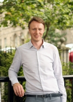
Walsh, John

Walsh, John
Assistant Head of School
Technological University Dublin

Walsh, John

Abstract
This presentation will look at the ways in which 3D printing is being used and taught at Dublin School of Creative Arts, TU Dublin. It presents a diverse range of 3D Printing / Additive Manufacturing projects and applications ranging from printing of Prosthetic Prostates and Tumours, to Drones, to Guitars and Sculptural Artefacts. While the context for the presentation will be in the field of Design and Creative Arts, the focus will be on how 3D printing can be used as a tool to solve a diverse range of problems.

Biography
John Walsh is Assistant Head of School and Lecturer in Product Design at Dublin School of Creative Arts, TU Dublin. He is founder of TU Dublin CreateLAB, which supports industry and entrepreneurs in the development of new products. He is also owner of Made Design Consultancy, a Juror at the iF Design Awards and is a Past-President of the Institute of Designers in Ireland.

3D Printing
TechSearch International, Inc. TechSearch International, Inc. Vardaman, Jan
Packaging Trends for AI
Vardaman, Jan

Vardaman, Jan
President
TechSearch International, Inc.

Vardaman, Jan

Abstract
Artificial Intelligence (AI) makes it possible for machines to learn from experience, adjust to new inputs and perform human-like tasks. AI or deep learning is expected to be applied to a wide range of applications, including connectivity or Internet of Things (IoT), big data processing and servers, cloud services, autonomous driving, 5G communications, smart factory or Industry 4.0, robotics, AR/VR. The package choice depends on many factors including design, density, reliability, and supply chain. This presentation examines the applications using AI and the packages in production today. The presentation also discusses future packages expected for these applications. Package choice, design, and materials impact and the importance of co-design will be discussed.

Biography
E. Jan Vardaman is president and founder of TechSearch International, Inc., which has provided market research and technology trend analysis in semiconductor packaging since 1987. She is the co-author of How to Make IC Packages (by Nikkan Kogyo Shinbunsha), a columnist with Printed Circuit Design & Fab/Circuits Assembly, and the author of numerous publications on emerging trends in semiconductor packaging and assembly. She is a senior member of IEEE EPS and is an IEEE EPS Distinguished Lecturer. She is a member of SEMI, SMTA, IMAPS, and MEPTEC. She received the IMAPS GBC Partnership award in 2012 and the Daniel C. Hughes, Jr. Memorial Award in 2018. She is an IMAPS Fellow. Before founding TechSearch International, she served on the corporate staff of Microelectronics and Computer Technology Corporation (MCC), the electronics industry’s first pre-competitive research consortium.

Advanced Packaging Conference
Techworks Techworks Banks, Alan
Banks, Alan

Banks, Alan
Chief Executive Officer
Techworks

Banks, Alan

Biography
Alan Banks – Chief Executive Officer - TechworksAlan Banks was appointed as Chief Executive Officer in March 2019Prior to his appointment as CEO he was most recently Chairman of the Automotive Electronics Systems Innovation Network (AESIN) a role he has held since 2012.Alan started his career at British Telecom where he trained as a Telecommunications Electronics engineer. He joined Ford Motor Company in 1985 where he held a number of management positions within the IT Department delivering Telecommunications and Product Development systems developing Ford products in Europe.After completing an International Service Assignment in the United States in the early 2000’s he returned to Visteon in the UK where he was the European IT Manager.He held a number of senior positions within Visteon delivering Vehicle Cockpit Electronic Programs and after 35years completed his career at Visteon as the Engineering Director responsible for delivering cockpit electronics for Ford and Jaguar Land Rover.Alan is a member of the UK Automotive Council’s Intelligent Connected and Mobility Working Group and is the lead for Power Electronics at the Automotive Council.He is passionate about growing Electronics capability and believes strongly that connected communities and collaboration are the key to exploiting successful partnerships enabling the exploration of the wealth of opportunity it brings with new and exciting emerging technology markets-

SMART Transportation Forum
Texas Instruments Texas Instruments Enzelberger-Heim, Michael
Automated Hardware Diagnosis and Qualification
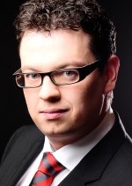
Enzelberger-Heim, Michael

Enzelberger-Heim, Michael
Process Engineer
Texas Instruments

Enzelberger-Heim, Michael

Abstract
One common challenge for Analog Wafer Fabs is the large variety of technologies, processes and products. Due to the long lifetime of analog products the product-mix and therefore the complexity of manufacturing processes typically increases over the years. This high complexity leads, together with usually mature toolsets, to a growing risk of misprocessing due to equipment weakness or failure. Based on these challenges and in light of increasing automation of production processes, we have developed a novel automatic hardware qualification scheme for crucial hardware functionalities.Our method allows to test and qualify vacuum integrity, plasma and gas flow parameters without any human interaction. It can either be run alongside regular process qualifications or while the tool and chambers are idle to assure maximum tool availability. The universal setup allows the implementation on fundamentally different toolsets like dielectric deposition or metal etch without any modification of the underlying routine. The high data density and coverage of this monitoring scheme facilitates root-cause analysis and the vast number of available small signals enables proactive reaction to upcoming failures.In this presentation, the implementation and data collection as well as the impact on the manufacturing and tool stability will be presented and discussed.

Biography
Dr. Michael Enzelberger-Heim is currently working as a process engineer in the Plasma/Thinfilm module of TI’s Freising Fab, responsible for PECVD, SACVD and ALD processes.Starting as a trainee at TI in 2014, Michael held different positions in product and process engineering. In 2018, he has been elected member of the group technical staff.Michael studied physics in Erlangen and Grenoble and holds a PHD in experimental physics from the FAU Erlangen in the field of Synthetic Carbon Allotropes.

Fab Management Forum
ThermoFisher Scientific ThermoFisher Scientific de Jong, A. Frank
Metrology platforms developments for enhanced productivity
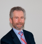
de Jong, A. Frank

de Jong, A. Frank
Director, Strategic Programs
ThermoFisher Scientific

de Jong, A. Frank

Abstract
In the present semiconductor industry, the importance of metrology is increasing as the demands on production are higher both from a complexity perspective, as well as from a cost-perspective.The complexity of novel generations of memory and logic devices is higher, both because dimensions are getting smaller and because device architectures are more complex, with 3D GAA transistors as an example. Some years ago metrology companies together with several academic institutes as well as the semiconductor RTO’s started the ECSEL project “3D Advanced Metrology” to explore especially the demands of the 3D architectures. This project, a predecessor to MADEin4, focused on new (platform) technology developments also combining several techniques to get better results faster. The project has recently been completed, and some of the results will be discussed.From a cost perspective, improved metrology functionality is absolutely necessary to decrease time-to-market of new generations of semiconductor devices and to increase the yield in mature processes. Relevant metrology results have to become available more quickly, and ready for further analysis to enable fast feed-back into production. In the MADEin4 project, the main challenge for the metrology platforms is formulated as follows:Develop new metrology platforms which can handle the higher complexity and smaller dimensions while at the same time enhance the productivity. The platforms have to be “Industry 4 ready” so that larger amounts of data can be acquired, processed and be available for further analysis.In this presentation, some examples will be discussed of what this means in terms of platform development. WP3 contains developments of in-line as well as off-line platforms, including metrology for front-end and back-end and advanced packaging. Apart from physical improvements, new data science techniques such as AI and ML are used to enhance the productivity of the platforms.

Biography
Frank de Jong received a PhD in physics from TU Delft. After working as scientist at the Philips Research Labs in Eindhoven, The Netherlands, he transferred to the Electron Optics division. He held various positions in R&D and then became responsible for the world-wide Research activities of FEI as director Research and Technology. In 2012, he became director of Technology Partnerships for FEI. Since FEI was acquired by Thermo Fisher Scientific in 2016, he is responsible for Strategic Partnerships in their Materials and Structural Analysis Division (MSD). Frank de Jong has a large experience in leading public-private partnerships, both internationally and in the Netherlands. Most of these projects are positioned at the transition point between academic research and industrial developments. He is the coordinator of the EU-ECSEL project 3DAM, and Work-package leader in the new EU-ECSEL project MADEin4. Frank de Jong serves in various public (national) functions, such as industrial leader for roadmap Nanotechnology, executive board of foundation NanoNextNL and advisory roles for Dutch science institutes Amolf and ARC-NL.

MADEin4 Session
TowerJazz TowerJazz Hirsch, Yoav
Industry 4.0 Digitization of Manufacturing for Enhanced Productivity
Hirsch, Yoav

Hirsch, Yoav
Project manager
TowerJazz

Hirsch, Yoav

Abstract
The vision of Industry 4.0 is achieving significantly higher productivity, efficiency, and self-managing production processes. This, by letting people, machines, equipment, logistics systems, and work-in-process components communicate and cooperate with each other directly. Digitizing the manufacturing floor will boost the endless strive to reduce machinery downtime, reduce the cost of quality and increase production efficiency. Many trends show that by 2020, 80% of large manufacturers will update their operations and operating models with IoT and analytic-based situational awareness to mitigate risk and speed time to marketDigitization of Manufacturing will increase the production efficiency of a complex manufacturing line by acting on different levels, from the initial study of the process (Virtual Commission) to the global control of the line ( Virtual Metrology, Predictive Maintenance and Prediction of Final Yield). It enables machines to interact socially within groups, with other machines (and/or humans), and to apply social skills to each robot in such a way that it will be able to interact with other robots, patriciate in a group, and collaborate to achieve joint tasks/goals without preprogramming.Digitization of Manufacturing enhances the Digital Twin concept, which provides a virtualized product that lets you analyze how a product performs under various conditions and make adjustments in the virtual world to ensure that the new physical product will perform exactly as planned in the field.Advanced image sensors are central players in both sides of this equation. Manufacturing of large format sensors is enabled by excellent and well monitored production line, while on the other end new capabilities of image sensor technology like 3D imaging (TOF), wider wavelength (from UV to NIR and SWIR), embedded processing within the sensors and large format sensors become key components in advanced production lines.

Biography
Mr. Yoav Hirsch serves as a leading project manager at TowerJazz CMOS Sensor business unit. As part of his role he is in charge of various image sensor technology projects, supporting the sensor’s business unit development roadmap. Mr. Hirsch has extensive experience in the semiconductors industry, specializing in the field of CMOS image sensor. Throughout his career, he held various positions in SCD, ECI-Telecom and AFCON-industries where he managed a variety of multi-disciplinary technology projects, which required, amongst others, expertise in the fields of industrial control, system engineering, manufacturing, and design electronics.Mr. Hirsch holds a B.Eng Electrical Engineering from Coventry University, England, M.Sc. in Electrical engineering from Tel-Aviv University and an MBA from Haifa University, Israel.

MADEin4 Session
Trymax-semiconductor Trymax-semiconductor Schaefer, Christian
UV Cure – an Enabling Process Technology for Efficient Thick Photoresist Drying
Schaefer, Christian

Schaefer, Christian

Trymax-semiconductor

Schaefer, Christian

Abstract
Completely dried photoresists (“PR”) masks are a necessary precondition to avoid undesired effects in subsequent manufacturing steps like high dose implant, metal/oxide etch and ash. But in particular for medium or thick PR commonly used in Power Device, MEMS or Advanced Packaging (TSV) this becomes increasingly difficult using just the standard thermal hard bake.A solution for achieving crosslinked PR films is the so-called UV Cure - a state-of-the-art technology combining UV exposure with precise low-high-low temperature cycling. This leads to 100% deep dried PR films due to crosslinking of the resin and the photo active compounds by UV radiation and thereby efficient solvent evaporation. The presentation will explain above physical-chemical phenomena, show the effects in key applications and will further explain the Trymax NEO 2000UV system requirements and features

Biography
Christian Schaefer is since January 2016 Sales Director North Europe for Trymax Semiconductor Equipment, the Netherlands. He has a MS in Process Engineering and a PhD in Material Science - both of the Technical University of Aachen, Germany. Before he joined Trymax he held positions in the semi equipment industry as BU Manager at PVA TePla AG in Munich (10y), as VP Sales & Board Member at EV Group in Austria (7y) and as Product Group and General Manager at Leybold Systems in Hanau, Germany (14y).

Exhibitor Presentations
TU Dresden IAVT TU Dresden IAVT Tiedje, Tobias
3D electronic packaging for IoT devices – from prototype to series production
Tiedje, Tobias

Tiedje, Tobias
Research Associate
TU Dresden IAVT

Tiedje, Tobias

Abstract
Rethinking electronic manufacturing - why do electronic components always have to be soldered onto a printed circuit board? Is it not possible to omit the printed circuit board at all and integrate the components directly into a single chip package instead? This was the question asked by Prof. Bock's team of four researchers at the Electronic packaging lab of the TU Dresden. The result is a manufacturing approach that saves around half of the process and design steps. Thereby, today’s and tomorrow’s challenges such as high-frequency transmission, cooling and miniaturization can be managed. The technology is called “connecting embedded components as a technological solution” – shortly KONEKT in German. The team around KONEKT raised the EXIST research transfer funding of the BMWi. This enables the production of adaptively manufactured 3D assemblies on large and competitive dimensions. The KONEKT-technology revolutionizes the electronic assembly by using 3D manufacturing and realizing high-frequency interconnects. It combines the possibility of producing individual packages of rapid prototyping and manufacturing at a large scale. Simplified processes facilitate fast and automated production of various assemblies. Therefore, energy, process and material costs will be reduced. Now, small and medium-sized companies have the opportunity to establish new business fields by ordering individual electronic packages without high set-up costs. During the EXIST-project the KONEKT team will establish a company, which will offer 'packaging-as-a-service'.Tobias Tiedje (KONEKT project manager): "With KONEKT a wide variety of products can be realized, starting from 3D-sensor systems as prototype up to RFIDs and high-frequency assemblies in series manufacturing for the Internet of Things (IoT). The clients will have much more possibilities in designing their product without limiting their creativity and innovation.”

Biography
Tobias Tiedje holds a degree in Electrical Engineering from TU Dresden. He held positions at the Electronics Packaging Laboratory at TU Dresden, including team lead of the junior research group „Communication infrastructure for atto networks in 3D chipstacks (Atto3D)“. Since May 2019 he leads the KONEKT project.Friedrich Hanzsch holds a BSc. in Accounting and Finance, MSc. in Resource Economics from Technische Universität Bergakademie Freiberg. He worked at DAS Environmental Experts GmbH as employee in Quality Management and joined KONEKT project in May 2019 as CMO.

3D Printing
Young Disruptors
Tyndall National Institute Tyndall National Institute Gunning, Fatima
Coherent photonic transmitters: what, how and when?

Gunning, Fatima

Gunning, Fatima
Senior Staff Researcher
Tyndall National Institute

Gunning, Fatima

Abstract
As capacity demands in optical communications continues to increase, and with standard single mode optical fibres (SMF) still prevailing as the main communications channel, techniques to maximise the spectral efficiency of SMF's available bandwidth are now moving from research to implementation. While DSP and higher order modulation formats are becoming widely available commercially, in particular for 400G-600G approaches, Tb/s capacities per transponder are likely to be achieved with multi-carrier schemes. In this talk, we will review the need for multi-carrier coherent transmitters, what they are and show potential configurations, discuss how to overcome foreseenble challenges, and especulate when this technology will be potentially ready.

Biography
Dr Gunning is a Senior Staff researcher and Head of Graduate Studies at Tyndall National Institute, and Senior Research Fellow at the Physics Department, University College Cork, Ireland. She worked previously at Corning Research Centre in UK, had several internships at British Telecom at Adastral Park in UK, and holds a Master and PhD degrees in Physics from Pontifícia Universidade Católica do Rio de Janeiro, Brazil. She was part of the team pioneering on Optical Coherent Wavelength Division Multiplexing (also known as “superchannels” or coherent transmitters) at Tyndall. Her current research focus on the development novel devices for high capacity systems at 1.5 and 2 microns wavelengths, and on incorporating adaptive physical layer solutions with Software Defined Networks for network efficiency, control and management. Dr Gunning collaborates closely with Tyndall’s semiconductor devices team on the next generation of integrated photonic devices, and incorporates high-speed testing at chip level in the lab. She also volunteers and leads initiatives to promote Science in the community, and in particular efforts to increase gender representation in Physics and Engineering at all levels. She’s the acting chair for Empowering Women Committee @ Tyndall, participates in UCC’s Athena Swan focus groups, champions Tyndall’s Centre of Integrated Photonics (IPIC) gender action plan and the IEEE Photonics Society as AVP for Multicultural Outreach.

Smart Photonics
U To top
ULVAC ULVAC Yamazaki, Yoshifumi
ULVAC solutions for new MEMS devicesULVAC solutions for new MEMS devices
Yamazaki, Yoshifumi

Yamazaki, Yoshifumi

ULVAC

Yamazaki, Yoshifumi

Abstract
As for MEMS applications, we show ULVAC`s PZT sputtering and etching processes. We also share Bio MEMS application by glass etching

Biography
Yoshifumi Yamazaki joined ULVAC, Inc, in 1990. Involved with semiconductor systems especially dry etcher, and ion implanter. Moved to ULVAC GmbH in 2018, as a Technical sales manager in Europe

Exhibitor Presentations
Umicore Umicore Steegen, An
Steegen, An

Steegen, An
CTO
Umicore

Steegen, An

Biography
Dr. An Steegen holds a Ph.D in Material Science and Electrical Engineering from the Catholic University of Leuven, KUL, in collaboration with the Interuniversity Microelectronics Center, IMEC, in Belgium. She joined IBM Semiconductor in Fishkill, New York, in 2000. As Semiconductor Technology R&D Director, she was responsible for IBM’s advanced logic technology development for the mobile and ASICS market and she served as host executive in charge of IBM’s International Semiconductor Development Alliance.In 2010, Dr. Steegen rejoined IMEC as Executive Vice President for Semiconductor Technology & Systems. She was in charge of IMEC’s technology portfolio and strategic innovation in the areas of ICT, health, entertainment, mobility and energy with partnerships across the entire semiconductor eco-system.’Dr. Steegen is recognized as leader in semiconductor R&D. She holds many patents and she is an acclaimed and inspiring thought leader in innovation in the IoT and digitalization era. She is a member of the SEMI Board of Industry Leaders and she is a frequently asked speaker at the semiconductor industry’s prominent conferences and events.Recently, Dr. An Steegen joined Umicore as Chief Technology Officer, responsible for the company’s overall innovation strategy and in charge of Umicore’s central R&D to ensure the business units technology leadership in the areas of clean mobility materials, recycling and sustainability. With her background, she will empower Umicore’s transformation in this age of accelerated digitalization.Dr. An Steegen is a member of the Board of Directors of Barco NV, Kortrijk, Belgium, since 2017.

SMART Workforce
Umicore Umicore Carl Quaeyhaegens, Carl Quaeyhaegens
Building a circular economy in the electronic manufacturing industry: the perspective of a material solution supplier.
Carl Quaeyhaegens, Carl Quaeyhaegens

Carl Quaeyhaegens, Carl Quaeyhaegens
Program Director
Umicore

Carl Quaeyhaegens, Carl Quaeyhaegens

Abstract
Responsible mineral sourcing and recycling are an integral part of the array of innovative solutions a material solution provider can offer to the semiconductor ecosystem. In this talk both the logic and the business sense will be explored that are driving the development of urban mining.

Biography
Alumni of London Business School and PhD in material science. Carl build-up a broad international experience in business development and in commercial and operational rolls at Umicore before assuming the role of general manager. Today Carl is Program Director at Umicore.

Building a Circular Economy in the Electronics Manufacturing Industry
United Nations Centre for Trade Facilitation and Electronic Business (UN/CEFACT) United Nations Centre for Trade Facilitation and Electronic Business (UN/CEFACT) Patchava, Anushka
Embracing Connectivity: Technologies Transforming the Digital Healthcare
Patchava, Anushka

Patchava, Anushka
Expert Advisor, Global Digital Health, AI and Blockchain Strategist
United Nations Centre for Trade Facilitation and Electronic Business (UN/CEFACT)

Patchava, Anushka

Abstract
Over the past decade, digital health technologies have been ever increasing in number and funding – with real opportunity to improve patient outcomes and practice efficiencies. This session highlights the changing role in healthcare – shifting from reactive to proactive, from sick care to health care system and shares a vision of Connected Care, a vision in which the electronics sector has a huge role to play. It outlines what is required to bring this vision to life, addresses the readiness of global markets for the adoption of new technologies and discusses how conscious collaboration between providers, payers, clinicians and other sectors can catalyse the move from vision to reality.

Biography
Dr Anushka Patchava is an experienced strategist having supported the commercialisation of several pharmaceutical assets and the implementation of digital strategies in the Healthcare and Lifesciences sector. Prior to this, Anushka received her Medical Degree from University of Cambridge, and has practiced in both the UK (NHS) and US (Harvard) health systems. She has a particular interest in architecting data-driven environments and is passionate about creating a Connected Care ecosystem; harnessing IoT, 5G, Blockchain and Digital Therapeutics to drive data-fluidity and improve patient outcomes.She has advised a variety of health related seed and early stage start-ups, drawing upon her unique experience to bridge the interface between physician, patient, payer and policy. She has worked across cross-functional and cross-sector teams, driving conscious collaboration and agile methodologies to disrupt legacy systems and behaviour with deliberate digital design.She holds qualifications in a breadth of areas including Digital Strategy and Leadership, Value Based Healthcare (Harvard Business School), Innovation (Stanford Business School), Digital Marketing and Analytics (Google Squared) and most recently, Intermediate Python.Her role as an healthcare expert advisor to the United Nations (CEFACT) is focused on Artificial Intelligence and Blockchain, and her ideas and experience will be shared in an upcoming book chapter on the role of Artificial Intelligence in Healthcare.

Opening Ceremony & Keynote
Univ. grenoble Alpes, CNRS, LTM Univ. grenoble Alpes, CNRS, LTM Pargon, Erwine
Si and SiN High-Q microresonators for quantum and nonlinear optics applications
Pargon, Erwine

Pargon, Erwine
Associate researcher
Univ. grenoble Alpes, CNRS, LTM

Pargon, Erwine

Abstract
Silicon is an attractive platform for correlated photon pairs sources that can be used for quantum cryptography and computing, while SiN On Insulator is promising for Kerr frequency comb source proposed in many nonlinear optics applications, such as on-chip spectroscopy, and terabit coherent communications. In both cases, high-Quality factor microresonators are required to get power-efficient nonlinear sources. The quality factor of the ring is directly correlated to the optical propagation losses caused by the material bulk or surface absorption, or scattering losses generated by roughness. In this work, we report on the fabrication and testing of Si and SiN microresonators with record values of quality factor.In sub-micrometric Si waveguides, scattering loss is the primary source of optical propagation losses. High temperature H2 annealing treatment was introduced in the fabrication process flow to minimize the Si sidewalls roughness at the atomic scale, enabling the fabrication of high intrinsic Q (>6 x 10⁵) Si micro-resonators for on-chip heralded single photon quantum sources by spontaneous four-wave mixing. On the other hand, the absorption loss due to residual NH bonds in the SiN is the limiting factor for achieving low loss SiN waveguide. By introducing high temperature N2 annealing treatment in the process fabrication, we demonstrate critically coupled SiN resonators with intrinsic quality factors of Q > 6x10⁶ using high-confinement waveguide dimensions (1.7-µm-wide, 820-nm-thick) with corresponding optical losses approaching 5 dB/m. The statistical study performed on 200mm wafer shows a variability of the optical results of 0.8% which proves the high reproducibility of the fabrication process. Using such high-quality factor devices, we report the possibility to generate Kerr frequency combs at sub-mW input powers coupled into the bus high-confinement waveguide.This work was supported by the the French National program IRT Nanoelec and the RENATECH network

Biography
Erwine Pargon is currently associate researcher at the “Laboratoire des Technologies de la Microélectronique” (LTM), a joint academic unit of the CNRS and Grenoble Alpes University in Grenoble, France. She received her M.S. in 2001 and Ph. D. in 2004 in Material Sciences from the University of Grenoble-Alpes. After a year of research at the Chemical Engineering department of UC Berkeley in USA, she joined in 2006 the LTM/CNRS located on the CEA/LETI site of Grenoble. At LTM, she has the capability to conduct applied research in a professional environment allowing unique partnerships with key players of the Microelectronics industry. Her research focuses on the development and characterization of plasma etching processes involved in the elaboration of advanced devices for microelectronic, photonics and photovoltaics applications. The common objective of her research work is the development of damage free plasma etching processes. In particular, she worked on an important issue in plasma patterning, the pattern sidewalls roughness, that affects device performances whatever the targeted applications. She proposed methods to characterize it accurately and to minimize it. She has co-authored more than 70 papers in peer reviewed journals and has participated to about 30 invited talks at international conferences. In 2010, she was awarded the Bronze Medal of CNRS for her research achievements. She led the LTM etch team from 2008 to 2010. She is a regular reviewer of several international journals (JVST, Plasma process and polymer, Microelectronic engineering..). She is a committee member of the “Advanced Etch Technology for Nanopatterning” conference of the SPIE since 2012, of the Plasma Etch and Strip in Microelectronics (PESM) workshop since 2013 and of the Plasma Science Technology Division of the AVS Symposium since 2017.

Smart Photonics
University College Dublin University College Dublin Russo, Giovanni
Cyber-Physical Human-in-the-Loop Systems for manufacturing: exploring the border between learning and control
Russo, Giovanni

Russo, Giovanni
Lecturer in Cyber-Physical Systems
University College Dublin

Russo, Giovanni

Abstract
Complex manufacturing systems can be modeled as Cyber-Physical Systems (CPSs). Essentially, a CPS is a system controlled via a closed-loop computer-based algorithm and tightly integrated with the communication infrastructure and the behavior of its users. In a manufacturing scenario, it is of particular interest to study CPSs that have humans in their loop. In this context, the talk we will present some recent results related to the design of the control system for such Cyber-Physical, human-in-the-loop, systems. In particular, we will start with introducing our main set-up and context for the research. Then, we will present a set of new results for controlling systems directly from data. From the conceptual viewpoint, the results will allow to learn a control policy from demonstrations and the idea deploy our algorithms in a manufacturing environment, where the plant is not programmed to execute a task but it rather learns how to execute it from success stories

Biography
Giovanni Russo is a Lecturer in Cyber-Physical Systems at University College Dublin (UCD). Dr. Russo received his Ph.D. degree from the University of Naples Federico II in 2010. The focus of the work was on the stability of nonlinear dynamical systems with applications to networked control and systems biology. In 2010, Dr. Russo joined Ansaldo STS as a System Engineer and, from 2012 to 2015, he was the Lead System Engineer and Integrator of the Honolulu Rail Transit Project (HRTP) – the first mass transit driverless railway system of the United States. From 2015 to 2018, after having completed the HRTP system-level design, Dr. Russo has been with IBM Research Ireland as a Research Staff Member in Optimization, Control and Decision Science. In September 2018, Dr. Russo joined UCD and current research interests include Cyber-Physical Systems, nonlinear dynamics, stochastic systems and networked control systems. Dr. Russo is currently a member of the Board of Editors of IEEE Transactions on Circuits and Systems I: regular papers and of the IEEE Transactions on Control of Network Systems. Dr. Russo is also a funded investigator of the Science Foundation Ireland Research Centres I-Form (Advanced Manufacturing Irish Research Centre) and LERO (Irish Software Research Centre).

Smart Manufacturing I (software-centric)
University of Bristol University of Bristol Michalopoulou, Eleni
Michalopoulou, Eleni

Michalopoulou, Eleni
PhD Student in the department of Chemistry and the Atmospheric Chemistry Research Group
University of Bristol

Michalopoulou, Eleni

Biography
Eleni has a background in physics, oceanography, environment and meteorology. As part of her undergraduate studies she worked for the Hellenic National Meteorological Service using satellite data and atmospheric modelling. She spent 2 years doing field work focusing on marine research where she focused on oceanography and anthropogenic pollutants (e.g. microplastics). In 2015 she started her PhD in atmospheric chemistry in the University of Bristol where she worked on quantifying perfluorocarbon emissions from the aluminium, semiconductor and rare earth smelting industries. Eleni is a co-author in the Intergovernmental Panel on Climate Change chapter on emissions from the metal industry. Finally, Eleni has been on developing multidisciplinary approaches and sustainable development with a particular focus on global challenges and development strategies.

SMART Workforce
University of Regensburg University of Regensburg Wegener, Joachim
Analytical Microtechniques to Monitor Cell and Tissue Phenotypes
Wegener, Joachim

Wegener, Joachim
Professor and Head of the 'Cell-Based Sensors' Division at Fraunhofer EMFT
University of Regensburg

Wegener, Joachim

Abstract
Many areas of personalized and regenerative medicine require performing in vitro experiments with patient-derived cell samples or tissue models generated from human stem cells (iPS). Typical examples are chemosensitivity testing of biopsy material or drug screening using human disease models. When these samples are studied in a laboratory environment, it is highly beneficial to use label-free and non-invasive physical techniques for monitoring their behavior as these approaches allow for time-resolved and repeated analysis as well as the later use of the samples for other assays. Several analytical micro-techniques will be discussed in this presentation that provide quantitative assessment of complex cell and tissue phenotypes like synchronous beating of heart muscle tissue, migration of cells during wound healing or respiration in three dimensional tissue models.

Biography
Joachim Wegener received his doctorate in 1998 from the University of Muenster and continued his scientific education as a postdoctoral fellow with Prof. Ivar Giaever at Rensselaer Polytechnic Institute in Troy (NY). In 2004 he obtained his „Habilitation“ at the University of Muenster, Germany. Since 2008 he is full professor for bioanalysis at the University of Regensburg (Germany).His research interests focus on interfacing animal cells with physical transducers (e.g. planar electrodes, piezoelectric devices, …) to monitor the cell response to chemical, biological or physical stimuli without using any labels. It is the paradigm of his research to replace classical concentration-analysis by effect-analysis on biological organisms.Besides his affiliation with the University of Regensburg, he is head of the division 'Cell-Based Sensors' of the Fraunhofer Research Organization.

SMART MedTech
University of Stuttgart, Institute of Semiconductor Engineering (IHT) University of Stuttgart, Institute of Semiconductor Engineering (IHT) Schulze, Jörg
SiGeSn – A new (old) building block for nano- and optoelectronic devices
Schulze, Jörg

Schulze, Jörg
Full Professor and Head of Institute
University of Stuttgart, Institute of Semiconductor Engineering (IHT)

Schulze, Jörg

Abstract
Recent years have seen a lot of experimental effort directed towards integrating photonics with electronics. The Group-IV elements Si and Ge are the dominating materials of semiconductor electronics. However, their application to optoelectronics is limited due to their indirect bandgap and the concomitant low efficiency in optoelectronic applications. Recent experiments have therefore focused on the investigation of GeSn and SiGeSn alloys that could potentially be used as direct bandgap Group-IV-materials for an efficient on-chip integration of photonics and electronics. The relaxed alloy Ge(1-y)Sn(y) has been predicted to become a direct bandgap material for y > 0.073, while pseudomorphic Ge(1-y)Sn(y) is predicted to have a direct bandgap for y > 0.19. A number of experimental studies have been performed to fabricate and characterize Ge(1-y)Sn(y) bulk and quantum well photodetector devices. Because of the large lattice mismatch between Ge and Sn (14 %), the growth of Ge(1-y)Sn(y) alloys with a large percentage of Sn is difficult to achieve on Si and Ge substrates. The ternary alloy SiGeSn allows one to decouple bandgap and lattice constant [8] and is, therefore, a particularly interesting candidate for optoelectronic applications. Several groups have reported the successful fabrication of SiGeSn alloys by Chemical Vapor Deposition and Molecular Beam Epitaxy; bulk SiGeSn-photodiodes have been fabricated and analyzed. Furthermore, a number of proposals concerning photonic devices such as light-emitting diodes or modulators with Multi-Quantum-Well structures in their active regions have been made. For those devices, additional advantages such as a lower intensity of Auger processes have been predicted. The talk presents results on the growth and characterization of SiGeSn alloys integrated on Si substrates and their use in optoelectronic devices.

Biography
Jörg Schulze studied experimental physics at the TU of Braunschweig, Germany. In 2000 he received his PhD in Electrical Engineering from the Electrical Engineering & Information Technology Faculty of the University of the German Federal Armed Forces Munich with a dissertation on Boron surface phases and Esaki-like tunneling transistors. From the same faculty he received in 2004 his post-doctoral degree (Habilitation) in Semiconductor Physics and Microelectronics. He was active as Senior Consultant for Technical Risk Management and as Head of Competence Field “Robust Design Optimization” in Siemens Corporate Technology (2005-2008). Since 2008 he has been working at the University of Stuttgart, Germany, as Professor of Electrical Engineering and Head of the Institute of Semiconductor Engineering. He authored more than 200 peer reviewed articles, two book chapters and two books.

Strategic Materials Conference
University of Twente University of Twente Zwanenburg, Floris
Ambipolar quantum dots in planar silicon
Zwanenburg, Floris

Zwanenburg, Floris
Associate Professor
University of Twente

Zwanenburg, Floris

Abstract
We create ambipolar quantum dots in planar silicon nanoscale transistors. We first investigate the conformity of Al, Ti and Pd nanoscale gates by means of transmission electron microscopy [1]. Next we define low-disorder electron quantum dots with Pd gates [2], and depletion-mode hole quantum dots in undoped silicon [3]. For the latter we use fixed charge in a SiO2/Al2O3 dielectric stack to induce a 2DHG at the Si/SiO2 interface. The depletion-mode design avoids complex multilayer architectures requiring precision alignment and allows directly adopting best practices already developed for depletion dots in other material systems. Finally, I will show ambipolar charge sensing: we have fabricated a single-electron transistor next to a single-hole transistor, and tuned both quantum dots to simultaneously sense charge transitions of the other quantum dot. Using active charge sensing the single-hole transistor can detect the few-charge regime in the electron quantum dot.[1] P. C. Spruijtenburg et al., Nanotechnology, (2018).[2] M. Brauns et al., Scientific Reports 8, 5690, (2018).[3] S. V. Amitonov et al., Applied Physics Letters 112, 023102 (2018).

Biography
Floris Zwanenburg (1976) studied applied physics at the TU Delft. In 2008 he received his PhD for research on semiconductor nanowires with Leo Kouwenhoven. As a post-doc at UNSW in Sydney he worked with silicon quantum dots. This system has a unique fabrication scheme offering unprecedented control over all relevant parameters, as he demonstrated by reaching the single-electron regime in a highly tunable Si quantum dot. With his team at UNSW he has also used this system to read out the spin of a single electron (Nature, 2010) and to create a nuclear spin qubit (Nature, 2013). In 2011, he returned to the Netherlands for a tenure track position at the University of Twente. After initial collaborative efforts with the Dzurak team from UNSW on silicon quantum-dot technology, his team has extended this design to an ambipolar circuit, with which he has defined electron and hole quantum dots in a single device. Since 2013 he has had a new project on quantum dots and superconductivity in Ge/Si core/shell nanowires. In the past ten years he has become an expert in silicon quantum electronics: the quantum mechanical behaviour of single electron or hole spins confined to (artificial) atoms in silicon.

Disruptive Computing
V To top
VAT Group VAT Group Gahler, Desiree
Gahler, Desiree

Gahler, Desiree
Global HR Business Partner and Head of Talent Development
VAT Group

Gahler, Desiree

Biography
Desiree Gahler is Global HR Business Partner & Head of Talent Development in VAT Group. In that role she sets the talent strategy and drives programs that ensure VAT’s long term business performance. As a strategic HR Business Partner she focuses together with the leadership team on ensuring sustainable and scalable organizational development and fostering a culture and environment that supports productivity, empowerment and engagement. She holds a masters degree in human capital management and brings a background from a multinational corporate environment.

SMART Workforce
Veeco Veeco Sundin, Phillip
Addressing Impact of Shrinking Line/Space Dimensions on PR Strip, UBM/RDL Etch and Wafer Thinning Processes


Sundin, Phillip

Sundin, Phillip

Veeco

Sundin, Phillip

Abstract
Moore’s law sharpened focus on shrinking gate dimensions to drive performance and cost. This paper explains emerging challenges as Moore’s law slows, with focus transitioning to the packaging side as the industry adopts heterogeneous integration and smaller line/space dimensions for better performance.Technical requirements are more challenging; e.g., the interconnect and bumping process flow is as follows: barrier/seed layer deposition, patterning, plating, photoresist (PR) strip, and etch. Designers are using redistribution layers (RDL) in flip-chip designs to redistribute I/O pads to bump pads without changing the I/O pad placement. Under bump metallization (UBM) enhances reliability by providing the critical interface between the metal pad and solder bump. Higher I/O density with improved reliability and performance also leads to shrinking line geometries (from >10µm to sub-1µm) along with smaller bump diameter and pitch. As a result, the photoresist becomes more difficult to remove, calling for more effective methods.Shrinking dimensions pose similar challenges in UBM/RDL etch. A critical requirement is to minimize undercut while removing barrier/seed layers. Higher undercut impacts mechanical integrity while insufficient removal leads to poor yield.As thinner devices also drive performance and/or optimized form factor, wafers get thinner in MEMS, Power, RF, Image Sensors. Grinding damages the wafer surface, leaving microcracks, residual stresses and edge chipping. A subsequent process is needed to repair the surface, reduce stress and achieve desired thickness. Wet processing has emerged as a preferred method for surface treatment and wafer thinning while offering higher uniformity at lower cost.This presentation explains technical results for PR strip, UBM/RDL etch and wafer thinning steps

Biography
It will be provided

Advanced Packaging Conference
Versum Materials Versum Materials Buchanan, Iain
Buchanan, Iain

Buchanan, Iain

Versum Materials

Buchanan, Iain

Biography
Iain Buchanan received his BSc in Chemistry from the University of Stirling and his PhD in Molybdenum Chemistry from the University of Manchester. He joined Air Products Electronics Division in 1995 which was subsequently spun-out as Versum Materials in 2016 and then acquired by Merck in 2019. He has filled a variety of technical marketing and business management roles and is currently a Manager of Strategic Marketing based in Scotland

Strategic Materials Conference
Vista Ventures, LLC Vista Ventures, LLC Hogan, Jim
Hogan, Jim

Hogan, Jim
Executive Managing Partner
Vista Ventures, LLC

Hogan, Jim

Biography
James H. Hogan, executive managing partner of Vista Ventures, LLC, is an experienced senior executive who has worked in the semiconductor design and manufacturing industry for more than 40 years. He serves as a member of the board of directors for electronic system design, intellectual property, semiconductor equipment, material science and IT companies.Previously, Hogan was general partner at Telos Venture Partners and served as chief technology officer and senior vice president of business development at Cadence, and chief operating officer of Smart Machines, a semiconductor equipment automation company. Earlier, he worked for National Semiconductor and Philips where he established device physics laboratories globally and manufacturing yield improvement programs.Hogan founded Heart of Technology (HOT), a philanthropic organization based in San Jose, Calif., to unite the semiconductor industry to aid charities in their fundraising efforts for the betterment of local communities and enrichment of lives.He holds Bachelor of Arts and Math, Bachelor of Science and Computer Science and MBA degrees from San Jose State University.

SMART Design
VTT VTT Aalto, Timo
Micron-scale low-loss silicon photonics for communication and sensing

Aalto, Timo

Aalto, Timo

VTT

Aalto, Timo

Abstract
This presentation gives an overview of the micron-scale silicon waveguide platform at VTT. This includes low-loss and polarization independent waveguides, components and photonic integrated circuits. Photonic integrated circuits (PICs) are primarily based on 3 µm thick silicon-on-insulator (SOI) waveguides, while some work is also done with 12 µm thick SOI waveguides. Latest results are provided about power-efficient switches and phase modulators, polarization splitters and rotators, and monolithic Ge photodiodes (up to 40 GHz). A path towards monolithically integrated, broadband isolators and high-speed modulators is shown. Some examples of III-V hybrid integration on SOI and optical I/O coupling are also given. This includes up-reflecting mirrors, which support wafer-level testing and packaging, as well as broadband anti-reflection coatings. Main focus will be on concepts that support dual-polarization and high-power operation over the continuous wavelength range from 1.2 to 1.8 µm, and also mid-infrared operation up to 5 µm wavelength.

Biography
Dr. Timo Aalto has worked at VTT since 1997 with the primary research focus on silicon photonics. He received his M.Sc. and D.Sc. degrees in optoelectronics technology from the Helsinki University of Technology in 1998 and 2004, respectively. He leads the Photonics Integration team that is the key user of VTT's clean room facilities in Espoo (Micronova) and Oulu. He has ~80 peer-reviewed journal and conference publications. He has reviewed EU projects, journal articles and theses, and written one book chapter. He has coordinated several large projects funded by EU, the European space agency, national funding organizations and industry.

Smart Photonics
W To top
World Economic Forum World Economic Forum Schwab, Olivier
Leadership in the Fourth Industrial Revolution
Schwab, Olivier

Schwab, Olivier
Managing Director
World Economic Forum

Schwab, Olivier

Abstract
Leadership in the Fourth Industrial Revolution

Biography
MSc in Civil Engineering, Ecole Polytechnique Fédérale de Lausanne and the Massachusetts Institute of Technology. 1999-2001, as Business Development Manager, Industry to Industry, San Francisco, an online business marketplace. 2003, Co-Founder, Club Airways, a pan-European airline charter service based in Geneva. 2002-03, consulting projects, Mercer Management Consultants. 2003-09, with Schindler Group, first as Assistant to the President, then as Manager, Logistics and Supply Chain for the company’s high-end product lines for the Asian market. With the World Economic Forum: 2010-11, led the Technology Pioneers Programme, Geneva;2011-2015, Executive Director, China, responsible for the development in the Greater China Region, based in Beijing; oversaw the development of relationships with leading Chinese businesses, government entities, and academic institutions; since Sept. 2015, Head of Business Engagement; leads the relationships with the Forum’s 1,000 business members and partners; responsibilities include ensuring that the Forum’s Partners are actively engaged in its various events and initiatives, and integrating them in the Forum’s various communities; also oversees the Technology Pioneers Programme aimed at young start-ups globally, and the Family Business Community.

Opening Ceremony & Keynote
X To top
X-FAB X-FAB Podewils, Mario
Podewils, Mario

Podewils, Mario

X-FAB

Podewils, Mario

Biography
Mario von Podewils, since October 2007 Operations Manager of the Wafer Fab at XFAB Erfurt, was born 1963 in Thuringia Germany. Since more than 35 years he is working in the semiconductor industry. Meanwhile he held several positions as Engineer and Team as well as Department Leader e.g. in the Thesys GmbH and in the XFAB GmbH in Erfurt, Germany. He holds an Engineer Degree in Technology of Electronic Components and a Diploma in Industrial Engineering.

Fab Management Forum
X-FAB MEMS Foundry X-FAB MEMS Foundry Ernst, Stefan
Medical is the next Automotive – the Advance of Silicon-based Microfluidics Technologies and Applications

Ernst, Stefan

Ernst, Stefan

X-FAB MEMS Foundry

Ernst, Stefan

Abstract
Silicon-based Microfluidics have paved the way for the advent of various new applications and technologies for the bio-medical market, such as next-generation DNA sequencing and synthesis, chip-based disease detection, lab-on-chip or cell arrays. Increasing requirements in system complexity and data handling demand for a growing level of integration. At the same time, the application space is highly fragmented, technology concepts and supply chains are complex and application-specific, and development cycles are typically very long. In order to overcome the related technical and commercial challenges for the industrialization, a scalable business model is required – based on standardization of the manufacturing process and design cycle.

Biography
Stefan Ernst, born 1980, holds a PhD in Physics from Dresden University of Technology.He joined X-FAB in 2011 and worked in various positions in Technology Development. Since 2017, Stefan is in charge of Product Marketing and Strategy at X-FAB’s Business Unit MEMS.

SMART MedTech
X-FAB MEMS Foundry GmbH X-FAB MEMS Foundry GmbH Leopold, Steffen
Clash of Generations? – Changing Motivations, Requirements and Communication Styles as Seen by Young Professionals
Leopold, Steffen

Leopold, Steffen
MEMS Process Development, Team Leader Acoustics
X-FAB MEMS Foundry GmbH

Leopold, Steffen

Abstract
“The price of doing the same old thing is far higher than the price of change.” (Bill Clinton)Our presentation focuses on three factors of a successful working environment as seen by the “Millennials”. Here, a mutual understanding on the motivation of young professionals, the requirements of today´s semiconductor industry as well as modern ways of communication are key for a successful collaboration across generations. Therefore, we are going to present selected scientific research and add examples of our own working experience. In the first part of this contribution we will emphasise the motivation of young professionals beyond a monthly salary and career-building. Here we critically review if and how buzz-words like work-life-balance, flexible-working, home-office and company child-care are implemented in the semiconductor industry. In the second part we change perspective and try to look from a baby-boomers perspective on requirements, which have to be fulfilled by young professionals in order to make a contribution in their organization. Here we will comment on strategies of filling the gap between academic education and the experience driven specialized knowledge of advanced manufacturing. In addition to that, we will show generation differences in soft-skills and where young professionals may struggle. In the last section we will show what communication can do for bridging the generation gap. Starting with the generation specific habits, we will critically review social media for businesses and explore opportunities enabled by modern communication and contact sharing such as virtual teams. The later one is the key factor of mastering challenges with increasing complexity, while bringing together experts with diverse field of knowledge and creativity.A change in working environment is needed, not only regarding modern communication, even if we have to pay for it. As Bill Clinton said, the alternative is more expensive.

Biography
Steffen Leopold is the leader of the Acoustics Group in MEMS process development at XFAB Erfurt. He received his degree in mechatronics at the Ilmenau University of Technology in 2008. In 2009 he joined the chair of Micromechanical Systems at Institute of Micro- and Nanotechnologies IMN MacroNano® in Ilmenau. His research topics were tunable optics based on aluminum nitride thin films and the fabrication of silicon nanostructures. In 2016 he received the PhD degree on his thesis “Aluminum nitride membranes for tunable refractive micro-optics”. In the same year he joined X-FAB MEMS Foundry GmbH in the field of MEMS process integration.

Fab Management Forum
X-FAB MEMS Foundry GmbH X-FAB MEMS Foundry GmbH Berthold, Theresa
Clash of Generations? – Changing Motivations, Requirements and Communication Styles as Seen by Young Professionals
Berthold, Theresa

Berthold, Theresa
Development Engineer
X-FAB MEMS Foundry GmbH

Berthold, Theresa

Abstract
“The price of doing the same old thing is far higher than the price of change.” (Bill Clinton)Our presentation focuses on three factors of a successful working environment as seen by the “Millennials”. Here, a mutual understanding on the motivation of young professionals, the requirements of today´s semiconductor industry as well as modern ways of communication are key for a successful collaboration across generations. Therefore, we are going to present selected scientific research and add examples of our own working experience. In the first part of this contribution we will emphasise the motivation of young professionals beyond a monthly salary and career-building. Here we critically review if and how buzz-words like work-life-balance, flexible-working, home-office and company child-care are implemented in the semiconductor industry. In the second part we change perspective and try to look from a baby-boomers perspective on requirements, which have to be fulfilled by young professionals in order to make a contribution in their organization. Here we will comment on strategies of filling the gap between academic education and the experience driven specialized knowledge of advanced manufacturing. In addition to that, we will show generation differences in soft-skills and where young professionals may struggle. In the last section we will show what communication can do for bridging the generation gap. Starting with the generation specific habits, we will critically review social media for businesses and explore opportunities enabled by modern communication and contact sharing such as virtual teams. The later one is the key factor of mastering challenges with increasing complexity, while bringing together experts with diverse field of knowledge and creativity.A change in working environment is needed, not only regarding modern communication, even if we have to pay for it. As Bill Clinton said, the alternative is more expensive.

Biography
Theresa Berthold studied material sciences at Technische Universität Ilmenau and Pontificia Universidad Católica del Perú and received her master degree (M.Sc.) in 2014. Afterwards she was a PhD student at the Institute of Physics and the Institute of Micro- and Nanotechnologies at Technische Universität Ilmenau and received her PhD degree in 2018. In her PhD she studied the gas interaction of indium oxide surfaces by photo electron spectroscopy. Currently, she is working at X-FAB MEMS Foundry GmbH as development engineer. Her research is focused on TSV (trough silicon via) development.

Fab Management Forum
X-FAB Semiconductor Foundries GmbH X-FAB Semiconductor Foundries GmbH Liebau, Matthias
Development of an Efficient Software-Backup-Management-System for Semiconductor Equipment Controllers
Liebau, Matthias

Liebau, Matthias
Equipment Engineer
X-FAB Semiconductor Foundries GmbH

Liebau, Matthias

Abstract
All semiconductor production equipment is controlled by different types of controllers, computers and dedicated developed software. An appropriate software backup system is very important to predict unscheduled machine downtimes.X-FAB developed and implemented a Software-Backup-Management-System (Software-BMS) based on a database which is able to register all different types of unique equipment computer information (hardware & software). The software images of these systems can also be stored in that data base. Additionally there was developed an algorithm to find the best interval at which backups should be created. With this tool, X-FAB was able to reduce unplanned downtime due to unpredicted data loss, which results in significant lower unplanned downtime due to software issues and in a very short payback period.

Biography
Matthias Liebau was born on 15th September 1981 and graduated from high school in 2000. Since 2002 Matthias works for X-FAB in Erfurt. From 2002 to 2005 he was in training for a mechatronics technician. After graduating in 2005, he worked as an equipment technician at the local fab maintenance team. From 2007 to 2011 Matthias also studied mechatronics. Since his final exam in 2011 Matthias works as an equipment engineer at the local equipment engineering team.

Fab Management Forum
Y To top
Yole Développement Yole Développement Jolivet, Emilie
5G enabler : Advanced Packaging

Jolivet, Emilie

Jolivet, Emilie

Yole Développement

Jolivet, Emilie

Abstract
5G will totally redefine how the radio frequency (RF) front-end interacts in-between the network and the modem and the new RF bands, sub-6 GHz, and mm-wave pose big challenges for the industry. LTE evolution has led to complex architecture in today’s mobile phones, mostly due to carrier aggregation and RF’s board area and available antenna space have been reduced, leading to a densification trend with more handset OEMs adopting power amplifier modules and implementing new technics, i.e. antenna-sharing between LTE and WiFi. More densification in front-end modules will be required to enable new band integration and without tight integration 5G NR in the mmWave spectrum won’t be able to deliver the multi-gigabit speeds that is the key USP of 5G. Advanced multi die SiP packaging holds a large set of key technologies to address all flavors of 5G requirements that will enable its implementation in mobile.Advanced packaging represents an opportunity to increase end-product value offering advantages both in the scaling and functional roadmaps. Fan-Out platforms are increasingly viewed as one of the top options amongst leading package technologies. Fan-Out Packaging technology is not only a bridge to the CPI mismatch in pitch size but it is also a solution for functional performance and package dimension. Fan-Out packaging is essentially adopted in Radar for Automotive, APE for Smartphones and now potentially Antenna-in-Package for 5G mmWave smartphones and stacked memories-on-substrate for HPCs. Currently, all key players of different business models have Fan-Out packaging solutions in the market with a strong emphasis on cost and performance trade-off between Panel-level vs Wafer-level processing.

Biography
Emilie Jolivet is Director of the Semiconductor & Software Division at Yole Développement (Yole), part of Yole Group of Companies. Emilie manages the expansion of the technical and market expertise of her team. In addition, Emilie’s mission focusses on the management of business relationships with semiconductor leaders and the development of market research and strategy consulting activities. With its previous collaborations at Freescale and EV Group, Emilie developed a core expertise dedicated to package & assembly, semiconductor manufacturing, memory and software & computing.Emilie Jolivet holds a Master’s degree in Applied Physics specializing in Microelectronics from INSA (Toulouse, France) and graduated with an MBA from IAE (Lyon, France).

Advanced Packaging Conference
Yole Développement Yole Développement Pizzagalli, Amandine
Equipment Manufacturing Trends: What to expect for More than Moore devices?
Pizzagalli, Amandine

Pizzagalli, Amandine
Technology & Market Analyst,Equipment & Materials - Semiconductor Manufacturing
Yole Développement

Pizzagalli, Amandine

Abstract
The overall semiconductor equipment market is worth several billion dollars. By contrast, lithography equipment for the MTM industry is a small niche representing millions of dollars.However, megatrend markets like fifth generation (5G) wireless technologies, electric vehicles, and advanced mobile devices demand miniaturization and extra functionality. These emerging applications push MTM devices to new levels of complexity, resulting in big investments. As a matter of fact, fabricating the next MTM device generation requires tools with new technical specifications. These are very different to the “More Moore” mainstream semiconductor industry with respect to resolution, overlay, depth of focus (DOF), wafer bow and backside alignment.The new lithography equipment market for MTM devices is mostly driven by Advanced Packaging. This sector accounts today for almost 60% of the overall MTM lithography tools market and will continue dominating this industry with stepper technology. Meanwhile, a high percentage of lithography equipment revenue for MEMS and Sensors, CIS and Power devices comes is generated by retrofitted tools coming from the legacy semiconductor industry. MEMS, Sensors and Power Devices have more relaxed specifications, so that mask aligner tools are sufficient at lower cost. However, megatrend applications are pushing devices with more stringent requirements, with lithographic features below 1µm. This would pave the way towards greater adoption of stepper or disruptive technologies.This presentation will highlight the status of the lithography equipment type used for More than Moore devices along with a more in-depth analysis of technology trends and impacts made by emerging applications.

Biography
Amandine Pizzagalli is a Technology & Market Analyst, Equipment & Materials - Semiconductor Manufacturing, at Yole Développement (Yole). Amandine is part of the development of the Semiconductor & Software division of Yole with the production of reports and custom consulting projects. She is in charge of comprehensive analyses focused on semiconductor equipment, materials and manufacturing processes.Previously, Amandine worked as Process engineer on CVD and ALD processes for semiconductor applications at Air Liquide. Amandine was based in Japan during one year to manage these projects.Amandine graduated from the engineering school, CPE Lyon (France), with a technical expertise in Semiconductor & Nano-Electronics and holds an electronics engineering degree followed by a master’s in semiconductor manufacturing technology from KTH Royal institute of technology (Sweden).She has spoken in numerous international conferences and has authored or co-authored more than 10 papers

Strategic Materials Conference
Market Briefing
Yole Développement Yole Développement Boulay, Pierrick
How next generation cars will impact the automotive industry?
Boulay, Pierrick

Boulay, Pierrick

Yole Développement

Boulay, Pierrick

Abstract
A vision shared by OEMs and Tier-1s is that next generation of cars will be more and more electric, autonomous and connected. To achieve these goals, automotive players will have to work on the electrification of vehicles that can be hybrid or 100% electric. They will also have to develop and integrate sensors like radars, cameras and LiDARs to increase the level of autonomy. Cars will be increasingly connected meaning that more and more software and AI will be needed as well as technology to connect cars to their environment.Stricter emission regulations, lower battery costs, and increasing consumer acceptance will create new and strong momentum for penetration of electrified vehicles in the coming years. The speed of adoption will be determined by the interaction of consumer pull and regulatory push, which will vary strongly at the regional and local level.The autonomous trend is pushed by the development of sensors to monitor the surroundings of the vehicle. To do that, sensors are continuously developed to increase resolution, frame rate and dynamic range for cameras. Radar manufacturers have also released products from short-range to long-range detection and new entrants are working on 4D radars to increase the level of resolution. Finally, the interest into LiDAR sensors is continuously increasing with different technologies being pushed by manufacturers.Finally all these sensors will need higher level of computation as the amount of data generated will boom in the next years. Therefore, the artificial intelligence is slowly but surely invading the automotive ecosystem through autonomous cars and infotainment applications/systems. On the connectivity side, V2X, pushed by the development of 4G/5G-based cellular communication, provides direct communication from the car to other vehicles and infrastructure, and does not involve network operators in the process.

Biography
As part of the Photonics, Sensing & Display division at Yole Développement (Yole), Pierrick Boulay works as Market and Technology Analyst in the fields of Solid State Lighting and Lighting Systems to carry out technical, economic and marketing analysis. Pierrick has authored several reports and custom analysis dedicated to topics such as general lighting, automotive lighting, LiDAR, IR LEDs, UV LEDs and VCSELs. Prior to Yole, Pierrick has worked in several companies where he developed his knowledge on general lighting and on automotive lighting. In the past, he has mostly worked in R&D department for LED lighting applications. Pierrick holds a master degree in Electronics (ESEO – Angers, France).

SMART Transportation Forum
Yole Développement Yole Développement Mouly, Jerome
Personalized Medicine: Toward Innovative Solutions to Meet Healthcare Challenges
Mouly, Jerome

Mouly, Jerome
Senior Analyst & Business Developer
Yole Développement

Mouly, Jerome

Abstract
Healthcare is moving towards profound transformation for better performance of medical care while reducing the cost. To reach objectives, healthcare system needs innovative solutions and disruptive technologies placing the patient in a more centric approach.Everything is starting from personalized diagnostics, leading to development in next generation sequencing (NGS) or liquid biopsy, the latter being a key enabler of personalized medicine in cancer care, taking into account the uniqueness of individuals in gene variations but also in environment and lifestyle.Pharmaceutical companies are very active in this field to generate precision drugs delivered at the right concentration, to the right patient and at the site of the disease. These companies have established strong networks with NGS company solution providers like Illumina or Oxford Nanopore to accelerate personalized drug discovery. The fleet of sequencing instruments is expected to more than double within a period of 5 years. At the sequencing flow cell consumable, it will be about 4.2 million units to be sold in 2024 with a compound annual growth rate of 21% from 2018 to 2024.Huge amount of data will be created by an increasing number of diagnostic tools, including also medical wearables, collecting patient vital signs. Sensors are key parts of the diagnostic instruments requiring high sensitivity, reliability and selectivity to reach medical grade. Closed-loop insulin pumps are an example of personalized and precision medicine applications adjusting the drug delivery to the patient needs, thanks to the connected sensor worn on the patient’s body.The presentation will unveil the latest development contributing to increase personalized and precision medicine approaches, with key technologies trends and related challenges, reinforcing the link between technology and medical world.

Biography
Jérôme Mouly serves as a Senior Technology & Market Analyst & Business Developer specialized in microtechnologies within the Photonics & Sensing activities at Yole Développement (Yole). Jérôme is supporting the development of strategic projects, following leading customers of the company.Since 2000, he is also engaged in more than 100 marketing and technological analyses for industrial groups, start-ups and institutes in the field of MEMS, BioMEMS, wearable & connected medical devices. Through its numerous activities at Yole, Jérôme is covering the whole microelectronic supply chain including manufacturing processes and devices development.Jérôme is also regularly involved in international conferences, giving presentations and delivering keynotes.Jérôme Mouly holds a Master of Physics from the University of Lyon (France).

SMART MedTech
Yole Développement Yole Développement Troadec, Claire
5G's impact on RF Front-End: from Telecom Infrastructure to Hand sets
Troadec, Claire

Troadec, Claire
Division Director, Power & Wireless
Yole Développement

Troadec, Claire

Abstract
The telecom infrastructure market has not moved much in the past decade interms of the value of operators’ investments. Customer pricing also keeps decreasing, and building new infrastructure keeps showing smaller and smaller returns on investments for telecom operators. In this context, an attempt to create new markets and enlarge operators’ reach to customers beyond hand sets created 5G.The global landscape at network level will not move much before 2025. But it will definitely change in terms of technology and antenna systems, thus completely restructuring the radiofrequency (RF) component industry. On one hand frequencies are going from less than 3 GHzto up to 6 GHz for macro deployments, while small cells exploit millimetre-wavelengths (mm-waves). Meanwhile RF line power levels in front-ends will decrease from a few hundred watts to down to a few watts in macro site antenna systems, thanks to massive MIMO and active antenna systems implementation.At Hand set level, the main phone manufacturers differentiate from each other on the RF field by adopting either an integrated or a discrete approach. The market leaders Samsung, Apple, as well as smaller OEMs such as Sony, LG, Google or ZTE are moving towards integration using complex RF modules from Broadcom, Skyworks, Qorvo, Qualcomm and Murata, while the markets challengers, Huawei, Xiaomi, Oppo and Vivo, which drive as much volume as the market leaders, differentiate by favouring a discrete approach whenever possible.In our presentation, we will review how 5G is reshaping the RF Front-End industry. We will explain the positioning of the main component and module suppliers and review the technology mix needed to support 5G (Bulk Silicon, SiGe, GaAs, RFSOI, GaN,…) both at Telecom Infrastructure level and Hand set level.

Biography
Claire Troadec is Director of the Power & Wireless Division at Yole Développement (Yole), part of Yole Group of Companies. These activities are covering power electronics, batteries & energy management, compound semiconductors and emerging materials and RF electronics.Based on her valuable experience in the semiconductor industry, Claire is managing the expansion of the technical and market expertise of Power & Wireless team. Daily interactions with leading companies allow these analysts to collect a large amount of data and cross their vision of market segments’ evolution and technology breakthroughs. In addition, Claire’s mission is focused on the management of business relationships with leading companies of this sector and the development of market research and strategy consulting activities inside the Yole group.Claire Troadec holds a Master’s degree in Applied Physics specializing in Microelectronics from INSA (Rennes, France). She then joined NXP Semiconductors, and worked for 7 years as a complementary metal-on-silicon oxide semiconductor (CMOS) process integration engineer at the IMEC R&D facility. During this time, she oversaw the isolation and performance boosting of CMOS technology node devices from 90 nm down to 45 nm. She has authored or co-authored seven US patents and nine international publications in the semiconductor field and managed her own distribution company before joining Yole Développement in 2013.

Technology for Communication
Z To top
Zelenograd NanoTechnology Center Zelenograd NanoTechnology Center Shaimardanova, Oksana
MEMS for IoT: transfer ideas into solutions. From local market to global industry.
Shaimardanova, Oksana

Shaimardanova, Oksana
Head of Business Development
Zelenograd NanoTechnology Center

Shaimardanova, Oksana

Abstract
Made by: Zelenograd nanotechnology Center

Biography
Oksana Shaimardanova, Head of business development в Zelenograd NanoTechnology Center (Moscow, Russia)Experience in business development for high tech innovations for 10 years. Provides support to entrepreneurs seeking to commercialize the results of its developments in nanotechnology and other tech industries by creating their own companies and assistance for start-ups funded by ZNTC. Responsible for the development programs of business and industrial cooperative enterprises in the project market of innovative companies and startups. Zelenograd Nanotechnology Center – one of the leading innovation R&D companies in the field of nano- and microsystem technologies. The main specialization of the center: sensors of physical and biological quantities; VLSI design through SoC technology; devices and equipment.

Russia on the Edge of Digital Transformation
Zenzic Zenzic Porter, Richard
Porter, Richard

Porter, Richard
Director Technology and Innovation
Zenzic

Porter, Richard

Biography
Richard Porter is Director of Technology and Innovation at Zenzic, defining and overseeing a £200m portfolio of investments to make the UK the global centre for testing and development of self-driving technologies, building on existing and delivering new capabilities, both physical and virtual. Previously Richard was Director of Research and Innovation at Highways England, UK Research Liaison to US DoD, Security policy advisor and crisis manager at FCO. Richard is always interested in new technologies and encouraging collaboration to deliver technologies to market quickly and effectively

SMART Transportation Forum
Zenzic Zenzic Cracknell, Mark
Cracknell, Mark

Cracknell, Mark
Head of Technology
Zenzic

Cracknell, Mark

Biography
Mark joined Zenzic as Head of Technology in 2018, he is leading on establishing a world-leading suite of test facilities called Testbed UK. Mark is the architect of the UK Connected and Automated Mobility Roadmap to 2030 which establishes an industry wide view of the future. He previously worked at TfL, supporting the London connected and automated Testbed amongst other Surface Transport roles. Mark is a Chartered Engineer and has a First-class degree in Electrical and Electronic Engineering from Southbank University.

SMART Transportation Forum
Zollner Elektronik AG Zollner Elektronik AG Hoffmann, Markus M.
Smart Manufacturing setups to achieve an AI based Digital Transmission within the EMS-industry
Hoffmann, Markus M.

Hoffmann, Markus M.
Head of Business Development Asia-Pacific
Zollner Elektronik AG

Hoffmann, Markus M.

Abstract
1) DIGITAL TRANSMISSION within the EMS INDUSTRYWhat are the everyday challenges of an EMS company?2) INDUSTRY 4.0 & MADE IN CHINA 2025How geopolitical frame-conditions influence technical progress3) METHODS & TOOLSValue Stream MappingDigital FactoryMTMDFx4) SUPPORT TECHNOLOGY & AUTOMATIZATIONDigital TwinAutomized components handlingAugmented RealityCo-Robotics Solution5) AI & DEEP LEARNING WITHIN EMSThe 4 V´s of big dataAI support for qualityDeep Learning and Big Data for Predictive Maintenance6) INDUSTRY 5.0 supported by AIOptimize RFP-processesUsing 5G to increase automatizationNew business modell arise from Big Data7) Executive SummaryWhat does AI mean for the EMS-sectorWhat transition is needed to keep up the pace

Biography
Markus M. Hoffmann has more than 15 years of experience within the EMS-market, focusing on global direct customer care management. Developed and established processes as overall head for involved operational units in Eastern Europe, Asia & North America, Markus has built key account relationships with new and existing customers mainly within the Semiconductor (front- and back end) business. His latest role in Zollner is to force deep engagement in the definition and pursuit process for the EMS market in the Asia Pacific Region. Markus pursues business in the dedicated geographical area and market in accordance with the assigned Business Unit’s strategy same as identify new potential Business for key-sectors like Railway, Aerospace, Healthcare & Semidconductor. Beside his activities at Zollner, Markus acts as an International Observer Columnist & Podcast Panelist for Chinese International Radio (CRI). Markus was also part in this years SEMICON SEA (Advanced Packaging Forum) & SEMICON Taiwan (SiP Global Summit) as a Speaker and Panelist, sharing his idead on Smart Manufacturing & Hetergenous Integration.

Smart Manufacturing II (hardware-centric)